Extraction of nitride trap density from stress induced leakage current in
silicon-oxide-nitride-oxide-silicon flash memory
Shaw-Hung Gu, Tahui Wang, Wen-Pin Lu, Yen-Hui Joseph Ku, and Chih-Yuan Lu
Citation: Applied Physics Letters 89, 163514 (2006); doi: 10.1063/1.2360180 View online: http://dx.doi.org/10.1063/1.2360180
View Table of Contents: http://scitation.aip.org/content/aip/journal/apl/89/16?ver=pdfcov
Published by the AIP Publishing
Articles you may be interested in
Metal-oxide-high- k -oxide-silicon memory structure using an Yb 2 O 3 charge trapping layer
Appl. Phys. Lett. 93, 183510 (2008); 10.1063/1.3021360
Analysis of electronic memory traps in the oxide-nitride-oxide structure of a polysilicon-oxide-nitride-oxide-semiconductor flash memory
Appl. Phys. Lett. 92, 132104 (2008); 10.1063/1.2830000
Impact of high-pressure deuterium oxide annealing on the blocking efficiency and interface quality of metal-alumina-nitride-oxide-silicon-type flash memory devices
Appl. Phys. Lett. 91, 192111 (2007); 10.1063/1.2812570
Trap generation in cycled hot-electron-injection-programed/hot-hole-erased silicon-oxide-nitride-oxide-silicon memories
J. Appl. Phys. 99, 044502 (2006); 10.1063/1.2172724
High-pressure deuterium annealing for improving the reliability characteristics of silicon–oxide–nitride–oxide–silicon nonvolatile memory devices
Appl. Phys. Lett. 85, 6415 (2004); 10.1063/1.1842363
This article is copyrighted as indicated in the article. Reuse of AIP content is subject to the terms at: http://scitation.aip.org/termsconditions. Downloaded to IP: 140.113.38.11 On: Thu, 01 May 2014 01:44:24
Extraction of nitride trap density from stress induced leakage current
in silicon-oxide-nitride-oxide-silicon flash memory
Shaw-Hung Gua兲 and Tahui Wangb兲
Department of Electronics Engineering, National Chiao-Tung University, Hsin-Chu, Taiwan
Wen-Pin Lu, Yen-Hui Joseph Ku, and Chih-Yuan Lu
Technology Development Center, Macronix International Company, Ltd., No. 16, Li-Hsin Road, Science Based Industrial Park, Hsin-Chu 30077, Taiwan
共Received 11 April 2006; accepted 26 August 2006; published online 20 October 2006兲
The authors propose a technique to extract a silicon nitride trap density from stress induced leakage current in a polycrystalline silicon-oxide-nitride-oxide-silicon flash memory cell. An analytical model based on the Frenkel-Poole emission is developed to correlate a nitride trap density with stress induced leakage current. The extracted nitride trap density is 7.0⫻1012 cm−2eV−1. They find
that nitride trapped charges have a rather uniform distribution in an energy range of measurement 共⬃0.2 eV兲. © 2006 American Institute of Physics. 关DOI:10.1063/1.2360180兴
Polycrystalline silicon-oxide-nitride-oxide-silicon 共SONOS兲 flash memories have received much interest in re-cent years for their simpler fabrication process and better scalability as compared to conventional floating gate flash memory.1,2 For SONOS cells, programed charges are stored in silicon nitride traps. The cell programming and retention characteristics are intimately related to nitride trap character-istics. Much research effort with respect to silicon nitride process optimization has been conducted to improve nitride trap properties. However, nitride trap characterization tech-niques are still very limited at present. Lundström and Svensson estimated a nitride trap density with a direct tun-neling model.3 Paulsen et al. employed a low-frequency 共⬍1 kHz兲 charge pumping technique to separate nitride traps from interfacial oxide traps by a difference in their time constants.4 Later, they extracted a nitride trap density from reverse modeling of threshold voltage共Vt兲 retention loss by
combining trap-to-band tunneling and thermal excitation of trapped electrons in a nitride.5,6All the above methods, how-ever, are restricted to ultrathin bottom oxides共1.5–2.5 nm兲. For today’s SONOS cells, for example, nitride-read-only-memory共NROM兲 共Ref.7兲 or Nitride-based multiple bits/cell
共Nbit兲 共Ref.8兲 technology, a thicker bottom oxide is usually
employed to improve data retention. No appropriate nitride trap characterization methods are available for these cells.
In this work, we observe a high-voltage stress induced gate leakage current in a large area SONOS capacitor. An analytical model to extract a nitride trap density from the stress induced leakage current is developed. The effects of programming window共⌬Vt兲 and stress condition on the
ex-traction result are evaluated. The nitride trap energy distribu-tion is also profiled.
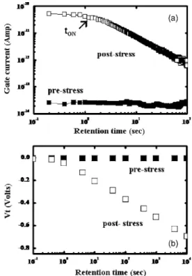
The SONOS capacitors used in this work have a 9 nm top oxide, a 6 nm silicon nitride, and a 5 nm bottom oxide. The capacitor area is 500⫻500m2. Uniform Fowler-Nordheim共FN兲 injection is employed for programming. The measured program-state gate leakage current versus retention time before and after a FN stress is shown in Fig.1共a兲. The FN stress is performed at Vg= −20 V for 1500 s. The
pro-gram Vtwindow is 3 V. The corresponding Vtretention loss
is shown in Fig. 1共b兲. A significant stress induced leakage current 共SILC兲 is observed in Fig. 1共a兲. Unlike in a metal oxide semiconductor capacitor, the SILC in a SONOS exhib-its a unique two-stage time dependence. In the first stage, the SILC exhibits a dc-like characteristic and in the second stage it follows a 1 / t time dependence. Our numerical simulation has shown that the first stage leakage current is limited by stress created oxide traps and the second stage is determined by the Frenkel-Poole 共FP兲 emission of nitride trapped electrons.9 According to the FP emission model, the nitride trapped charge emission time is
a兲Electronic mail: [email protected] b兲Electronic mail: [email protected]
FIG. 1. 共a兲 Measured gate leakage current in a large area SONOS 共500 ⫻500m2兲 at V
g= 0 V. The stress condition is Vg= −20 V for 1500 s. Both
devices are programed to an identical threshold voltage window of 3 V.共b兲 Corresponding Vtretention loss for the two samples.
APPLIED PHYSICS LETTERS 89, 163514共2006兲
0003-6951/2006/89共16兲/163514/3/$23.00 89, 163514-1 © 2006 American Institute of Physics This article is copyrighted as indicated in the article. Reuse of AIP content is subject to the terms at: http://scitation.aip.org/termsconditions. Downloaded to IP:
e共A*T2兲−1exp共共− q共qE/兲1/2兲/kT兲 =
⬘
exp共/kT兲,共1兲 where A* is the Richardson constant, is the nitride trap
energy measured from the conduction band edge, E is the electric field,
⬘
is the proportionality constant, and other variables have their usual definitions. In the FP emission lim-ited condition共second stage兲, the electron occupation factor 共f兲 of a nitride trap state with an energy has a retention time dependence as follows;5,6f共兲 = exp关− t/e共兲兴 = exp关共− t/
⬘
兲exp共−/kT兲兴. 共2兲Because the above double exponential changes abruptly from 0 to 1 aroundf=共kT兲ln共t/
⬘
兲, f共兲 can be approximated bya step function at=f and thusfis referred to as the FP
emission front hereafter. This approximation translates into a “clear-cut” picture; at a certain time t, trap states above the emission front f are completely emptied while the states
belowf are occupied by electrons. The FP emission front
moves downward in SiN band gap with a speed of df/ dt
= kT / t, or 2.3kT/decade of time. The nitride charge leakage current in the second stage therefore can be expressed as
Ig= AqNt共f兲df/dt = AqNt共f兲kT/t 共3a兲
and the nitride trap density can be extracted as
Nt共f兲 = Igt/AqkT. 共3b兲
Since the emission front stays almost unchanged in the first stage共f=0兲 and begins to move at the onset time 共ton兲 of
the second stage with a constant speed in a log共t兲 scale, the relationship betweenf and retention time t is readily
ob-tained,
f=0+ kT ln共t/ton兲, 共4兲
where0is the emission front in the first stage and is
deter-mined by the total amount of programed charges. From our numerical simulation, 0 is estimated to be 0.8 eV for the
present SONOS structure and programming window.9From Eqs.共3兲 and共4兲, the nitride trap density is characterized, as shown in Fig. 2. The solid line is directly from the SILC 关Fig. 1共a兲兴 and the dashed line is extrapolated from the Vt
shift 关Fig. 1共b兲兴. Notably, Fig. 2 reveals that the trapped charges have a rather uniform distribution over an energy range of measurement共⬃0.2 eV兲.
To further verify our nitride trap profiling technique, we change the FN stress condition and programming window. Figure3shows the SILC for two different FN stresses. The two samples have the same programming window and thus the same 0. It can be shown that the effective time for
nitride trapped charges at the emission front to escape from the ONO film9,10
eff= e共f兲 +c共f兲 c共f兲 ox⬇ e共f兲 c共f兲 ox, 共5兲
wheree共f兲 andc共f兲 represent the electron emission time
and capture time between the emission front and the nitride conduction band.oxis the conduction band electron
tunnel-ing time via stress induced oxide traps. The lightly stressed sample共B兲 has a lower first-stage dc leakage because of less oxide trap creation and thus a longerox. It is worth pointing out that the SILC in the two samples共A and B兲 converges in the second stage. The reason is that thefof the two samples
at a certain time in the second stage is only shifted by
KT ln共ton共B兲/ton共A兲兲⬃0.06 eV. As mentioned earlier, the
ni-tride trap density Ntis almost a constant in the measurement
range. The leakage current, which is proportional to Nt 关Eq.
3兴, is therefore nearly the same in the second stage regardless of stress conditions.
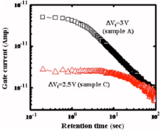
In addition, the SILC for different program windows is shown in Fig.4. The program window is 3 V for sample A and is 2.5 V for sample C. Sample A has a smaller 0 for more programed charges. According to the
Shockley-Read-FIG. 2. Extracted nitride trap density distribution vs relative nitride trap energy.0is estimated to be 0.8 eV共Ref.9兲.
FIG. 3. Measured SILC in two differently stressed samples. Sample A is stressed at Vg= −20 V for 1500 s and sample B is for 5 s. The programming
window is 3 V.
FIG. 4. Measured SILC for two different programming windows. Samples A and C are stressed under the same condition共Vg= −20 V for 1500 s兲 but
have program windows of 3 and 2.5 V, respectively.
163514-2 Gu et al. Appl. Phys. Lett. 89, 163514共2006兲
This article is copyrighted as indicated in the article. Reuse of AIP content is subject to the terms at: http://scitation.aip.org/termsconditions. Downloaded to IP: 140.113.38.11 On: Thu, 01 May 2014 01:44:24
Hall theory,e/c⬀exp共/ kT兲 and the difference in 0
be-tween samples A and C can be estimated from the ratio of the SILC in the first stage, i.e.,
SILC共first stage兲 ⬀ 1/eff⬀ exp共−0/kT兲
and
0共A兲 −0共C兲 = − kT ln共SILC共A兲/SILC共C兲兲. 共6兲
The0difference is still small. Consequently, samples A
and C have almost the same leakage current in the second stage because Nt共兲 can be considered as a constant for such
small0 difference. The extracted nitride trap density from
samples A–C is listed in TableI. The extracted result is in reasonably good agreement without regard to stress condi-tion and programming window.
In summary, a simple and reliable nitride trap profiling technique for a thicker bottom oxide SONOS is developed.
We find that a SILC in a SONOS exhibits a distinguished two-stage feature. The nearly 1 / t dependence in the second stage suggests that the nitride traps have a uniform energy distribution. The extracted nitride trap density is around 7.0 ⫻1012cm−2eV−1
The authors would like to acknowledge financial support from NSC, Taiwan under Contract No. NSC 94-2215-E-009-004. They would also like to thank the Technology Develop-ment Center of MXIC for providing technical support.
1M. H. White, IEEE Circuits Devices Mag. 16, 22共2000兲.
2M. H. White, D. A. Adams, J. R. Murray, S. Wrazien, Yijie Zhao, Yu
Wang, B. Khan, W. Miller, and R. Mehrotra, Symposium on NVM
Tech-nology共2004兲, p. 51.
3K. I. Lundström and C. M. Svensson, IEEE Trans. Electron Devices 19,
826共1972兲.
4R. E. Paulsen, R. R. Siergiej, M. L. French, and M. H. White, IEEE
Electron Device Lett. 13, 627共1992兲.
5Y. Yang and M. H. White, Solid-State Electron. 44, 948共2000兲. 6Yu Wang and M. H. White, Solid-State Electron. 49, 97共2005兲. 7B. Eitan, P. Pavan, I. Bloom, E. Aloni, A. Frommer, and D. Finzi, IEEE
Electron Device Lett. 21, 543共2000兲.
8Tahui Wang, W. J. Tsai, S. H. Gu, C. T. Chan, C. C. Yeh, N. K. Zous, T.
C. Lu, Sam Pan, and Chih-Yuan Lu, Tech. Dig. - Int. Electron Devices Meet. 2003, 169.
9S. H. Gu, Tahui Wang, Wen-Pin Lu, Yen-Hui Joseph Ku, and Chih-Yuan
Lu, IEEE Trans. Electron Devices共to be published兲.
10C. Main, S. Reynolds, and R. Brüggemann, Phys. Status Solidi C 5, 1194
共2004兲. TABLE I. Extracted nitride trap density from samples A, B, and C,
respec-tively, by using our technique.
Sample Nt共cm−2eV−1兲
A 7.1⫻1012
B 6.3⫻1012
C 6.2⫻1012
163514-3 Gu et al. Appl. Phys. Lett. 89, 163514共2006兲
This article is copyrighted as indicated in the article. Reuse of AIP content is subject to the terms at: http://scitation.aip.org/termsconditions. Downloaded to IP: 140.113.38.11 On: Thu, 01 May 2014 01:44:24