IEEE ELECTRON DEVICE LETTERS, VOL. 35, NO. 12, DECEMBER 2014 1233
Improvement of Resistive Switching Uniformity
for Al–Zn–Sn–O-Based Memory Device
With Inserting HfO
2
Layer
Po-Tsun Liu, Senior Member, IEEE, Yang-Shun Fan, and Chun-Ching Chen
Abstract— This letter demonstrates the characteristics of a resistive switching memory [resistive random access memory (RRAM)] device with a bilayer structure of aluminum–zinc–tin-oxide (AZTO) and HfO2-film layers. As for the RRAM operation, the formation and rupture processes of the conductive filaments can be confined in the HfO2layer with low-concentration oxygen vacancy. The resistive switching stability and electrical uniformity of bilayer AZTO/HfO2RRAM device are obviously enhanced as compared with the one only with a single layer of AZTO film. In addition, a physical mechanism for uniformity improvement is proposed by the localized conduction of conducting filaments. Index Terms— Resistive switching, RRAM, AZTO, localized conducting filament.
I. INTRODUCTION
M
ETAL oxide-based resistive random access memory (RRAM) has recently become an appealing technology for future memory applications, owing to its simple struc-ture, high storage density, low power consumption and fast switching operation [1]–[3]. In recent research, a transparent amorphous metal oxide semiconductor (TAOS) – an Al-doped zinc tin oxide (AZTO) film, acting as the resistive switching layer of a RRAM device – was reported to exhibit a remarkable resistance switching characteristic [4], [5]. The a-AZTO film does not comprise rare elements such as indium and gallium, and so is less costly than others. With respect to RRAM-related research, various technologies have been proposed to improve the uniformity and stability of resistive switching by confining conductive filaments using, for example, embedded nanocrys-tals [6], a bi-layer structure [7], and doping effects [8]. The element, hafnium (Hf) has a high electronegativity of 1.3, and so is a superior oxygen binder that is used to provide the desired electronic properties [9]. Motivated by the afore-mentioned features of RRAM, this investigation studies the brand-new Ti/AZTO/Pt device with an inserted HfO2 filmas a base layer. A low operation current can be achieved at 100 µA, and the uniform statistical distribution of resistive
Manuscript received September 16, 2014; revised October 2, 2014 and October 13, 2014; accepted October 13, 2014. Date of publication October 24, 2014; date of current version November 20, 2014. This work was supported by the Ministry of Science and Technology, Taiwan, under Contract 100-2628-E-009-016-MY3 and Contract 103-2221-E-009-010-MY3. The review of this letter was arranged by Editor D. Ha.
The authors are with the Department of Photonics, Institute of Electro-Optical Engineering, National Chiao Tung University, Hsinchu 30010, Taiwan (e-mail: [email protected]).
Color versions of one or more of the figures in this letter are available online at http://ieeexplore.ieee.org.
Digital Object Identifier 10.1109/LED.2014.2363491
switching parameters can be clearly presented. Also, this letter provided substantial material analysis to study the correlation between the oxidation states of chemical elements and the electrical uniformity. Additionally, AZTO-based nonvolatile memory devices enable the easy integration of backplane technology with a-AZTO thin film transistors (a-AZTO TFT) in the emerging transparent flat-panel displays (FPDs) for low-power system-on-panel (SoP) applications [5].
II. EXPERIMENTAL
Two RRAM devices were fabricated and investigated. The first device had the Ti/AZTO/Pt structure, and the other had the Ti/AZTO/HfO2/Pt structure. Both were fabricated at room
temperature without any thermal annealing. To fabricate an RRAM structure with a single switching layer, a 50 nm-thick AZTO resistive switching layer was deposited on a Pt bottom electrode (BE)/Ti/SiO2/Si substrate by
radio-frequency (RF) magnetron sputtering. An AZTO ceramic plate that contained Al2O3, ZnO and SnO2in a 3:67:30 mol % ratio
was the sputtering target. Both the 15 nm-thick HfO2
layer and the 35 nm-thick AZTO layer were sequentially deposited on another Pt/Ti/SiO2/Si substrate to form a
bi-layer of AZTO/HfO2 RRAM device structure. Finally,
the 20 nm-thick Ti top-electrode was sputter-deposited and patterned through a shadow mask with a diameter of 200µm. Electrical measurements were made using Keithley 4200 semi-conductor characterization analyzer. A voltage was applied to the Ti electrode, and the Pt electrode was grounded as a reference. Material analysis was conducted using transmission electron microscopy (TEM) and X-ray photoelectron spec-troscopy (XPS) to characterize the films.
III. RESULTS ANDDISCUSSIONS
Figure 1(a) compares the bipolar current-voltage characteristics of the Ti/AZTO/Pt RRAM device and the Ti/AZTO/HfO2/Pt device with a 35 nm-thick AZTO and a
15 nm-thick HfO2bi-layer in DC sweeping mode, respectively.
A set process change from the high-resistance state (HRS) to the low-resistance state (LRS) under positive voltage and a reset process from the LRS to the HRS was observed under a negative voltage. As presented in the inset in Fig. 1(a), the bi-layer RRAM device can be operated at 10 µA for low-power device applications following optimization of the AZTO/HfO2 thickness (HfO2 layer: 15nm → 5nm, 0741-3106 © 2014 IEEE. Personal use is permitted, but republication/redistribution requires IEEE permission.
1234 IEEE ELECTRON DEVICE LETTERS, VOL. 35, NO. 12, DECEMBER 2014
Fig. 1. (a) Typical I-V characteristics of RRAM devices with a single AZTO resistive switching layer and the 35 nm AZTO/15 nm HfO2bi-layer structure, respectively, under a DC sweeping mode. The inset shows the bipolar current-voltage characteristic of the RRAM with bi-layer structure at a compliance current of 10µA. (b) The statistical distribution of resistive switching parameters of the resistance of HRS and LRS, and (c) the statistical distribution of Vset and Vresetin both of single AZTO structures and bilayer structures during 100 continuous operation cycles.
Fig. 2. (a) Retention properties of the RRAM with AZTO/HfO2 bi-layer structure in LRS and HRS at 85 °C. (b) The stable endurance cycles of the Ti/AZTO/HfO2/Pt device.
AZTO layer: 35nm → 10nm) and oxygen content (Ar: 10sccm → Ar: 10sccm + O2: 2sccm). The statistical
distributions of resistance and operating voltages of the Ti/AZTO/Pt and Ti/AZTO/HfO2/Pt devices after
100 cycles of electrical operation are examined and presented in Fig. 1(b) and (c), respectively. The Ti/AZTO/HfO2/Pt
device exhibits superior uniformity on the HRS and the LRS. Figures 2(a) and (b) show the data retention and cycling endurance, respectively, of the Ti/AZTO/HfO2/Pt
RRAM device after process optimization, which exhibits a favorable resistive switching characteristic with a large
(>100) resistance window read at 0.2V for 104 s at 85 °C. The bi-layer RRAM device can passes the fast switching test at 500 ns, with a stable 107cycling endurance.
The improved uniformity of the Ti/AZTO/HfO2/Pt device
can be attributed to the difference in the concentration of oxygen vacancies and the Gibbs free energy of the oxi-dation reaction process of the AZTO/HfO2 interface. The
Gibbs free energy for the formation of HfO2 is
report-edly −1010.8 kJ/mol at room temperature [10]. However, the energy for the formation of SnO2, which has the
lowest free energy in the AZTO layer, is estimated to be
−515.8 kJ/mol [11]. Based on the equilibrium of the Gibbs
free energy across the interface between AZTO and HfO2, the
oxidation reaction in the HfO2 layer is inferred to proceed
more easily than that in AZTO layer. The oxygen at the interface between AZTO and HfO2spontaneously moves from
the AZTO layer to the HfO2 layer. XPS analysis can be
utilized to study the oxidation-included modification of the characteristics of an RRAM device. Figure 3(a) displays the cross-sectional TEM image of the Ti/AZTO/HfO2/Pt device.
A thin HfO2 layer is clearly observed between the Pt bottom
electrode and the AZTO layer. Figure 3(b) shows several sites of interest, including a, b, and c in the single-layer AZTO structure and the AZTO/HfO2bi-layer structure, respectively.
Figures 3(c) and (d) show the Sn 3d signal in the XPS spectra that corresponds the sites indicated in Fig. 3(b). As the depth increases from point a to c, the binding energy of the AZTO/HfO2bi-layer structure declines, revealing that the
oxidation of the Sn element in the single AZTO layer is much more complete than that in the AZTO/HfO2 bi-layer. The
insets of Figs. 3(c) and (d) present the ratio of the areas under the SnO2 (∼487 eV) and SnO (∼486.4 eV) signals at point
c, obtained by fitting the binding energy of the XPS peaks. The oxygen in the AZTO layer tends toward the HfO2 layer,
resulting in the formation of few oxygen vacancies in HfO2.
As a result, in the bi-layer devices, the conducting filament is localized in the HfO2 region after an initial forming process
for the bi-layer devices [12].
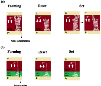
Figure 4 proposes the physical mechanism of the improve-ment of the resistive switching characteristics. When a positive bias is applied to the top Ti electrode of the RRAM device with a 50 nm-thick AZTO single layer, O2− from the AZTO
LIU et al.: IMPROVEMENT OF RESISTIVE SWITCHING UNIFORMITY FOR Al–Zn–Sn–O-BASED MEMORY DEVICE 1235
Fig. 3. (a) The cross-sectional TEM image of Ti/AZTO/HfO2/Pt devices. (b) Schematic drawing of 35 nm-thick AZTO/15 nm-thick HfO2 bi-layer structures (Left) and 50 nm-thick AZTO single layer structures (Right). (c) Sn XPS spectra of bi-layer structures, the inset showing the percentage of SnO2 and SnO by fitting the spectra peak. (d) Sn XPS spectra of AZTO single layer structure, the inset showing the percentage of SnO2and SnO by fitting the spectra peak.
Fig. 4. Schematic resistive switching mechanism of RRAM devices with (a) 50 nm-thick AZTO device, and (b) 35 nm-thick AZTO/ 15 nm-thick HfO2 bi-layer device.
layer moves upward and further oxidizes the Ti to form a top TiOx layer. Meanwhile, oxygen vacancies move downward,
bridging the conducting filament path from the top electrode to the bottom electrode. A messy accumulation of conductive filaments is likely form, since the process of formation is not merely local. In the following SET process, irregular conduction paths may be randomly formed because of the lack of restriction of the process of formation, as displayed in Fig. 4(a). Electrons can randomly pass through the con-duction paths, producing non-uniform resistance. As for the Ti/AZTO/HfO2/Pt structure with an equivalent 50 nm-thick
resistance switching layer RRAM device. An initial forming process can generate a localized conducting filament in the
HfO2region. Figure 4(b) schematically depicts the formation
of localized filaments in the HfO2 layer, which further
actu-ate the upper AZTO layer to form relatively small amount localized filaments. Hence, the electrons can be transported more regularly in the subsequent RESET and SET processes. Therefore, the Ti/AZTO/HfO2/Pt device has excellent resistive
switching characteristics.
IV. CONCLUSION
In summary, this letter developed a bi-layer resistive switch-ing layer in the form of an AZTO/HfO2 film for use in
RRAM nonvolatile memory. The Ti/AZTO/HfO2/Pt RRAM
device exhibits more uniform resistive switching and a more uniform setting/reset voltage than an RRAM device with a single AZTO resistive switching layer. Also, the bi-layer memory device has a fast switching time of 500 ns and exhibits robust bi-stable resistance switching behavior over 107 of switching cycles; it also exhibits stable retention character-istics for over 104 s at 85 °C. The improvement in resistive
switching characteristics is attributed to the formation of the localized conducting filament within the bi-layer resistive switching layer. This letter provides a simple method for enhancing the uniformity resistive switching characteristic for next-generation non-volatile memory applications.
REFERENCES
[1] R. Waser et al., “Redox-based resistive switching memories— Nanoionic mechanisms, prospects, and challenges,” Adv. Mater., vol. 21, nos. 25–26, pp. 2632–2663, Jul. 2009.
[2] K. Nomura et al., “Room-temperature fabrication of transparent flexible thin-film transistors using amorphous oxide semiconductors,” Nature, vol. 432, no. 7016, pp. 488–492, Nov. 2004.
[3] T.-M. Tsai et al., “Origin of hopping conduction in Sn-doped silicon oxide RRAM with supercritical CO2 fluid treatment,” IEEE Electron Device Lett., vol. 33, no. 12, pp. 1693–1695, Dec. 2012.
[4] Y.-S. Fan et al., “Bipolar resistive switching characteristics of Al-doped zinc tin oxide for nonvolatile memory applications,” Appl. Phys. Lett., vol. 101, no. 5, pp. 052901-1–052901-3, Jul. 2012.
[5] D.-H. Cho et al., “Transparent Al–Zn–Sn–O thin film transistors prepared at low temperature,” Appl. Phys. Lett., vol. 93, no. 14, pp. 142111-1–142111-3, Oct. 2008.
[6] W.-Y. Chang et al., “Improvement of resistive switching characteristics in TiO2 thin films with embedded Pt nanocrystals,” Appl. Phys. Lett., vol. 95, no. 4, pp. 042104-1–042104-3, Jul. 2009.
[7] J. Lee et al., “Effect of ZrOx/HfOx bilayer structure on
switch-ing uniformity and reliability in nonvolatile memory applica-tions,” Appl. Phys. Lett., vol. 97, no. 17, pp. 172105-1–172105-3, Oct. 2010.
[8] H. Zhang et al., “HfOx/TiOx/HfOx/TiOxmultilayer-based forming-free
RRAM devices with excellent uniformity,” IEEE Electron Device Lett., vol. 32, no. 4, pp. 566–568, Apr. 2011.
[9] C.-J. Kim et al., “Amorphous hafnium-indium-zinc oxide semicon-ductor thin film transistors,” Appl. Phys. Lett., vol. 95, no. 25, pp. 252103-1–252103-3, Dec. 2009.
[10] J. Lee et al., “Effect of ZrOx/HfOx bilayer structure on
switch-ing uniformity and reliability in nonvolatile memory applica-tions,” Appl. Phys. Lett., vol. 97, no. 17, pp. 172105-1–172105-3, Oct. 2010.
[11] J.-Y. Jung et al., “Effect of ionization characteristics on electro-chemical migration lifetimes of Sn-3.0Ag-0.5Cu Solder in NaCl and Na2SO4 solutions,” J. Electron. Mater., vol. 37, no. 8, pp. 1111–1118, Aug. 2008.
[12] D.-Y. Lee, T.-L. Tsai, and T.-Y. Tseng, “Unipolar resistive switching behavior in Pt/HfO2/TiN device with inserting ZrO2 layer and its 1 diode-1 resistor characteristics,” Appl. Phys. Lett., vol. 103, no. 3, pp. 032905-1–032905-4, Jul. 2013.