Investigation of Random Telegraph Signal with PD SOI MOSFETs
Ching-En Chena, Ting-Chang Changb, Hung-Ping Loa, Szu-Han Hoa, Wen-Hung Lob,
Tseung-Yuen Tsenga, Osbert Chengc, and Cheng Tung Huangc
a Department of Electronics Engineering, National Chiao Tung University, Hsinchu,
Taiwan, R. O. C.
b Department of Physics, National Sun Yat-Sen University, Kaohsiung, Taiwan, R. O. C.
c Device Department, United Microelectronics Corporation, Tainan Science Park, Taiwan,
R. O. C.
A novel method, called random telegraphy signal (RTS), was constructed to characterize the gate oxide quality and reliability of metal-oxide-semiconductor field-effect-transistors (MOSFETs). With the aggressive scaling of device size, drain current RTS (ID
-RTS) become a critical role in carrier transport of MOSFETs. Besides, RTS in gate leakage current (IG-RTS) was denoted as the
other new method to understand property of gate oxide. Recently, the study of RTS has also been made in MOSFETs with metal gate and high dielectric constant (metal gate/high-k). However, the RTS in partial depleted silicon-on-insulator MOSFETs (PD SOI MOSFETs) has not comprehensively been studied yet. This paper investigates RTS characteristics in PD SOI MOSFETs.
Introduction
Silicon on insulator (SOI) MOSFETs have been attracted huge attention recently because of it lower power consumption, good soft-error immunity, increased circuit packing density and absence of CMOS latch-up (1-5). However, the self-heating effect (6-7) and floating body effect (FBE) (9) are the inherent disadvantages in SOI devices. In conventional FBE is attributed to the excess hole were generated by impact ionization in saturation region with floating body condition. The new FBE is in linear region, called gate-induced floating-body effect (GIFBE) due to the aggressive scaling gate oxide thickness induced by gate tunneling current (10-12, 25). Similarly, when device scale down to deep sub-micrometer the random telegraph noise (RTN) or so-called random telegraph signal (RTS) will be observed and influence device dynamic performance (8, 22). The RTS phenomenon is commonly related to a carrier capture and emission behaviors. Recently, RTS has been considered as a major concern in scaling digital device because fluctuation of drain current amplitude (ΔID) will disturb analysis of signal
(13-15). In the deep sub-micrometer MOSFETs device, it is possible to exist one or few oxide traps near the SiO2/Si interface which were distributed over the vicinity of Si surface Fermi level. These traps can be investigated by RTS (16). The high and low level
states of drain current (ID) vary randomly with time, which correspond to the carrier
capture and emission at an oxide trap near the SiO2/Si interface. The average time at high level state of drain current corresponds to average capture time < τc > which means how
long will carrier be captured into the trap. On the other hand, the average time at low level state of drain current corresponds to average emission time < τe > represent how
long will carrier be emitted from the trap. Furthermore, RTS is very sensitive to local potential in channel near the trap. The average capture and average emission time ratio, < τc >/< τe > can be expressed by SRH model, which can be used to extract the local
potential change and defect position distribution (17-19, 21). Therefore By analysis of RTS, the gate oxide characteristics could be investigated. In this article, we used PD SOI n-type MOSFETs (n-MOSFETs).
Motivation
The noise stability issues have become much more complicated and compatible with device operation signal when device scale down to deep sub-micrometer. With the
aggressive scaling of device size, drain current RTS (ID-RTS) become a critical role in
carrier transport of MOSFETs (15, 20). In ID-RTS measurements, the gate and drain bias
supply will affect average capture time < τc > and average emission time < τe >, thus high
and low level state ratio in drain current < τc >/< τe > will change with different bias
supplies. On account of SRH model, trap location in MOSFETs can be extracted by the bias dependence of capture and emission time in ID-RTS analyses. In this paper, we focus on 65nm technology PD SOI n-MOSFETs. Furthermore, in PD SOI MOSFETs under floating body operation, the kink effect will appear to influence device stability (23-24). Recently, “linear kink effect” (LKE) is considered as one of serious issues for
SOI MOSFETs in linear region with floating body. Therefore, by using ID-RTS
measurement, this paper compares RTS characteristics of PD SOI devices under GB and FB operations.
Experimental Procedure
Using 65-nm SOI CMOS technology, PD SOI n-type MOSFETs (n-MOSFETs) are employed with a T-gate structure to investigate the gate induce floating body effect mechanism. The distance from the body contact to the active region is 0.35 µ m. The silicon film and buried oxide thicknesses for the devices are 75 and 145 nm, respectively. The gate oxide with a thickness of 12 Å was grown by in situ steam generation, with the channel doping concentration being about 3 × 1018 cm-3. The channel currents follow in the <110> direction on (100) substrates. In this letter, devices with a channel width (W)
of 0.5 µm and a length (L) 0.1 µm were selected for ID-RTS. The device structure is
showed in figure 1 (a) and (b).
Here, Using the Agilent-B1530A Waveform-Generator/Fast-Measurement-Unit
(WGFMU) to measure RTS as shown in figure 1 (c). For measuring ID-RTS in PD SOI
n-MOSFETs, devices were operated in linear region. The gate voltage was applied from
VG=0.35V to 0.65V. And drain voltage was applied from VD=0.05V to 0.2V and
sampling rate was 200/sec during 20sec ID-RTS measurement time at room temperature
(30℃) (4000 points were measured during measurement). The source and body
electrodes were grounded during measurement. For different measurement conditions, we
changed temperatures to 30, 50, 70 and 90℃ to analyze ID-RTS in PD SOI n-MOSFETs
respectively. Furthermore, for analyzing kink effect, ID-RTS were measured in PD SOI
n-MOSFETs under GB and FB operations. All the ID-RTS and current-voltage (I-V)
characteristics were measured by using Agilent B1530A WGFMU and Agilent B1517A high resolution source/monitor unit (HRSMU) respectively.
Figure 1. (a) Schematic shows the cross section of PD-SOI n-MOSFETs device. (b) ID
-RTS measurement system
Results and Discussion
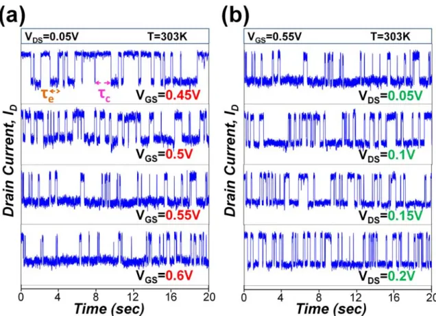
In the beginning, applied constant VD=0.05V in fast I/V mode and applied different
VG biases in PG mode from 0.4V to 0.65V respectively. Then ID-RTS was measured ID
sampling in a period of 20sec. We could find that when increased VG the corresponding
average capture time (< τc >) decreased and average emission time (< τe >) increased was
shown in figure 2 (a). In another condition, applied constant VG=0.55V in PG mode and
applied different VD biases in fast I/V mode from 0.05V to 0.2V respectively to sampling
ID in a period of 20sec ID-RTS measurement was shown in figure 2 (b). Obviously, we
observed that corresponding < τc > increased when increased VD. Meanwhile, the
Figure 2. Time domain ID-RTS evolution under (a) fixed VD=0.05V with different VG
from 0.45V to 0.6V and (b) fixed VG=0.55V with different VD from 0.05V to 0.2V in a
period of 20 sec.
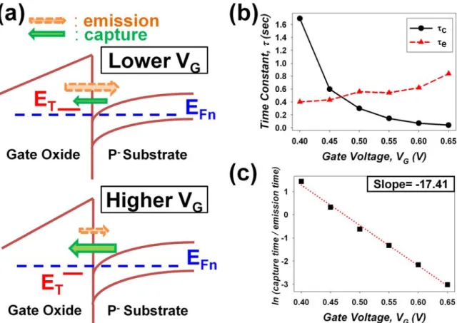
These ID-RTS characteristics as the above mentioned can be ascribed to the difference
between the oxide trap energy level and substrate surface Fermi energy level. According
to SRH model, 1/< τe > can be considered as probability of average electron emission
(average emission rate) and 1/< τc > represents probability of average electron capture
(average capture rate). As a result, < τc >/< τe > represents ratio of carrier occupancy
probability in substrate surface to oxide trap. In figure 3 (a), at the lower VG condition,
oxide trap energy level is above substrate surface Fermi energy level (electron quasi-Fermi energy level) due to the lower oxide field. Therefore, electrons occupancy probability in oxide trap is less than in substrate surface. This behavior is responsible for a higher < τc >/< τe > in figure 2 (a) at lower VG condition. On the other hand, at the
higher VG condition, oxide trap energy level is below substrate surface Fermi energy
level due to the higher oxide field. Hence, electrons occupancy probability in oxide trap is more than in substrate surface. This behavior is responsible for a lower < τc >/< τe > in
figure 2 (a) at higher VG condition. As a result, the change of < τc > and < τe > with
respect to VG is shown in figure 3 (b)
In fact, the ratio of < τc > to < τe > can be expressed in SRH model. Owing to the < τc
> and < τe > change with different gate and drain bias supplies, which can extract oxide
trap physical vertical location (XT) from substrate surface, physical lateral location (YT)
from source side and trap energy (ET). The corresponding equation was shown as below
(17)
Where k is a Boltzmann constant, T is the temperature, < τc > and < τe > are average
capture and emission time, respectively, g is a degeneracy factor, ET is trap energy level ,
EF is Fermi energy level. According to eq.[1] it also can be expressed as below (8)
XT = Tox * (kT/q)* - d[ln(<τc>/<τe>)]/dVg [2]
Where XT is location from substrate surface, Tox is oxide thickness. The change of ln(<
τc >/< τe >) with respect to VG was shown in figure 3 (c) can extract the physical vertical
locationby using the VG dependence of ln(< τc >/< τe >).It found that the oxide trap at
approximately 5.43A from substrate surface.
Figure 3. (a) Energy band diagram of PD-SOI MOSFETs device at different VG bias
supplied. (b) The change of < τc > and < τe > with different VG from 0.4V to 0.65V. (c)
The average time ratio of capture to emission, < τc >/< τe > changed at different VG.
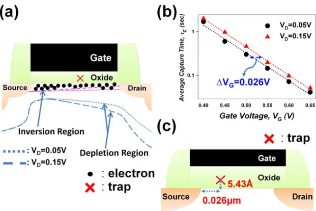
Next, according to SRH statistics, the average capture time can be expressed as below < τc > = 1 / (n * vth * σ) [3]
Where n is channel electron concentration, vth is thermal velocity, σ is the trap cross
section including tunneling and activated process. Therefore, at different VD influence,
the < τc > could be affected by different channel electron concentration due to the change
of potential in channel near the trap (21). Figure 4 (a) shows the cross section, different distribution of depletion and channel inversion region at VD=0.05V and 0.15V in lateral
direction. The depletion region near drain side becomes larger when VD changed from
increase. This behavior is responsible for a high < τc >/< τe > in figure 2 (b) at higher VD
condition. Therefore, the lateral location (YT) of trap can be extracted by ID-RTS at
different VD condition. Figure 4 (b) shows the change of < τc >/< τe > at VD=0.05V and
0.15V in the same region of VG from 0.4V to 0.65V. The ∆VG in figure 4 (b) means the
potential difference caused by different VD near trap position, namely the requirement of
VG for the same channel electron concentration as well as < τc >. As a result, the trap
lateral location by ID-RTS analyses mentioned above was shown in figure 4 (c) shows the extracted trap location according to ID-RTS analyses.
Figure 4. (a) Schematic shows cross section, distribution of depletion and channel inversion region in lateral direction at VD=0.05V and 0.15V respectively. (b) The change
of < τc > at VD=0.05V and 0.15V with different VG. (c) Trap location according to ID
-RTS analyses.
Then, ID-RTS were measured at different measurement temperatures to examine the
defect capture and emission behavior with respect to different temperatures. Applied
VG=0.35V and VD=0.2V, changed temperature from 30℃ to 90℃. The ID-RTS in
different temperatures was shown in figure 4. Obviously, when temperature increases, < τe > become smaller and more complicated. It is because the trapped electron received
more energy with respect to the higher temperature, and the trapped electron has more opportunity to overcome the barrier height of trap. Thus emission behavior is much fast
in high temperature rather than room temperature. When temperature increased to 90℃
drain current become instable, because of some thermal activity influence ID-RTS. It’s
Figure 5. ID-RTS varied with different temperature from 30C to 90C. Emission behavior
become much fast when increased temperature, it’s also lead to complicated signal to analyze.
GIFBE is a new serious issue in SOI MOSFETs due to the aggressive scaling gate oxide thickness induced by gate tunneling current (10-12, 25). As shown in inset of figure 6 GIFBE mechanism can be ascribe to several gate tunneling current, such as electron valance band tunneling (EVB) (10, 11) or anode hole injection (AHI) by hole valance band tunneling (HVB) (12, 25). LKE caused by GIFBE is owing to excess holes accumulate in the body in linear region. It lead to source barrier lowing thus threshold voltage (VTH) lowing, at the same time, ID increase and influence characteristics in ID-VG
mechanism due to the EVB mechanism requires higher VG let conduction band of gate
below valance band of substrate rely on band diagram as shown in inset of figure 6. By
using ID-RTS measurement under grounded-body (GB) and floating body (FB) operation
condition in order to find out the GIFBE influence stability of SOI MOSFETs.
Figure 6. ID-VG and gm-VG for a PD SOI n-MOSFET under GB and FB operations. The
inset shows the schematic diagram of three mechanisms of gate current for an ultrathin
gate oxide of a PD SOI n-MOSFET. Because the second peak of gm exhibits at VG=1.2V,
the GIFBE is likely attributed to HVB mechanism due to the EVB mechanism requires higher VG let conduction band of gate below valance band of substrate.
Here, applied VG=1.1 and 1.2V, VD=0.05V, it can be find the normal ID-RTS in PD
SOI devices under GB condition as shown in figure 7 (a). Then, applied same voltage to gate and drain terminal for ID-RTS under FB condition. Obviously, the ID signal is much
different from GB to FB conditions as shown in figure 7 (b). In FB condition, ID raises
with increasing measurement time. But ID is not infinitely rising with time. In this case,
ID will saturate around 47µA and 50.5µA in VG=1.1, 1.2V, respectively. Moreover, ID
signal become faster to reach saturation condition and sawtooth-like signal emerge much
frequently in higher VG as shown in figure 7 (b). This abnormal phenomenon in ID-RTS
may caused by GIFBE, however the mechanism of this behavior is not confirmed clearly. In the future, the abnormal phenomenon will be study in systematic operation conditions.
Figure 7. (a) Normal ID-RTS at VG=1.1V, 1.2V and VD=0.05V under GB operation. (b)
Comparing ID signal FB operation with GB, an abnormal RTS was observed under FB
operation. The signal varied much frequently in higher VG.
Conclusion
In summary, when device scaling down to deep sub-micrometer, noise become one of serious issue of MOSFETs device. Average capture time< τc > and emission time < τe >
vary with different VG as well as VD, which can be used to extract physical vertical and
lateral location, XT and YT of a oxide trap by SRH model for PD SOI n-MOSFETs.
Increasing the temperature, the electron can get energy to overcome trap barrier height. The electron emission behavior is easier to happen, which results in a complicated condition in analyses of ID-RTS. Furthermore, the investigation of ID-RTS for PD SOI
n-MOSFETs under floating body condition was found an abnormal drain current signal.
This abnormal noise affects the original analyses of ID-RTS and may cause a worse
influence than RTS in SOI MOSFETs. In the future, this abnormal noise will be study continuously.
Acknowledgments
Part of the work was performed at the United Microelectronics Corporation. The work was supported by the National Science Council under Contract NSC 100-2120-M-110-003.
References
1. Y. Kado, M. Suzuki, K. Koike, Y. Omura, and K. Izumi, Dig. Tech.
1992 Symposium on VLSI Circuits, 44 (1992)
2. Y. Hirano, T. Iwamatsu, K. Shiga, K. Nii, K. Sonoda, T. Matsumoto, S. Maeda, Y. Yamaguchi, T. Ipposhi, S. Maegawa, and Y. Inoue, Proc. Symp. VLSI Technology
Dig. Tech., 48–49 (2002)
3. Rodbell, K.P. Heidel, D.F. Tang, H.H.K. Gordon, M.S. Oldiges, P. Murray, C.E., Trans. Nucl. Sci., 54, 2474-2479 (2007)
4. P. Oldiges, K. Bernstein, D. Heidel, B. Klaasen, E. Cannon, R. Dennard, H. Tang, M. Ieong, and H.-S. P. Wong, Proc. Symp. VLSI Technology, Dig. Tech., 46–47 (2002)
5. C. C Chang, L. C Chen, Mater. Lett., 32, 287-290 (1997)
6. L. Su, J. E. Chung, D. A. Antoniadis, K. E. Goodson, and M. I. Flik, IEEE Trans.
Electron Devices, 41, 69-75 (1994).
7. S. Polonsky and K. A. Jenkins, IEEE Electron Device Lett., 25, 208-210 (2004). 8. K. K. Hung, P. K. Go, C. Hu, Y. C. Cheng, IEEE Electron Device Lett., 11, 90
(1990)
9. Dongwook Suh and J. G. Fossum, in IEDM Tech. Dig., 661–664 (1994).
10. A. Mercha, J. M. Rafi, E. Simoen, E. Augendre, and C. Claeys, IEEE Trans.
Electron Devices, 50, 1675–1682 (2003).
11. J. Pretet, T. Matsumoto, T. Poiroux, S. Cristoloveanu, R. Gwoziecki, C. Raynaud, A. Roveda, and H. Brut, in Proc. ESSDERC, 515–518 (2002).
12. C. H. Dai, T. C. Chang, A. K. Chu, Y. J. Kuo, F. Y. Jian, W.H. Lo, S. H. Ho, C. E. Chen, W. L. Chung, J. M. Shih, G. Xia, O. Cheng, and C. T. Huang, IEEE
Electron Device Lett., 32, 847–849 (2011).
13. J. W. Wu, J. W. You, H. C. Ma, and C. C. Cheng, C. S. Chang, G. W. Huang, T. Wang, Appl. Phys. Lett. 85, 5076-5077 (2004)
14. O. R. DIT BUISSON, G. GHIBAUDO and J. BRINI, Solid-State Electronics, 35, 1273-1276 (1992)
15. N. B. Lukyanchikova, M. V. Petrichuk, N. Garbar, A. Mercha, E. Simoen, Appl.
Phys. Lett. 94, 4461-4469 (2003)
16. M. Trabelsi, L. Militaru, N. Sghaier, A. Souifi, N. Yacoubi, Solid-State
Electronics,56, 1-7 (2011)
17. M. J. Kirton and M. J. Uren, Advance In Physics 38, 367-468 (1989)
18. S. Lee, H. J. Cho, Y. Son, D. S. Lee, H. Shin, in IEDM Tech. Dig., 1-4 (2009) 19. N. Tega, H. Miki, T. Osabem, A. Kotabe, K. Otsuga, H. Kurata, S. Kamohara, K.
Tokmi, Y. Ikeda, and R. Yamada, in IEDM Tech. Dig.,1-4 (2006)
20. Zhongming Shi Mieville, J.-P. Dutoit, M., IEEE Trans. Electron Devices, 41, 1161-1168 (1994)
21. H.C Ma; Y.L Chou; J.P Chiu; Y.T Chung; T.Y Lin; T. Wang; Y.P Chao; K.C Chen; C.Y Lu; IEEE Trans. Electron Devices, 58, 623-630 (2002)
22. Kenichi Abe, Takafumi Fujisawa, Akinobu Teramoto1, Shunichi Watabe, Shigetoshi Sugawa, and Tadahiro Ohmi1, Jpn. J. Appl. Phys., 48 04C044 (2009) 23. J.-P Colinge.; IEEE Electron Devices Lett., 9, 97-99 (1988).
24. J. Tihani and H. Schlotterer., IEEE Trons. Electron Devices, 22, 1017-1023, (1975)
25. C. H. Dai, T. C. Chang, A. K. Chu, Y. J. Kuo, S. C. Chen, C. C. Tsai, S. H. Ho, W. H. Lo, Guangrui Xia, Osbert Cheng, and Cheng Tung Huang, IEEE Electron