行政院國家科學委員會專題研究計畫成果報告
有機-高介電複層薄膜電晶體
計畫編號:NSC 97-2221-E-009-018-MY2
執行期限:97 年 8 月 1 日至 98 年 7 月 31 日
主持人:林鵬 國立交通大學材料科學與工程學系
一、中文摘要
本計畫以有機合成方式,改良過去文獻中 所發表 naphthalene-diimide (NTCDI-R)這類的傳 電子型有機半導體材料。然而,實驗成果上也 經由有機分子的單晶 x-ray 解析,去瞭解分子排 列堆疊時所呈現出的真實型態。透過單晶結構 分析,發現當分子取代基之中若含有強拉電子 基原子,則分子與分子之間會因極性的關係而 拉近了彼此之間的距離,進而增加有機半導體 的穩定性。此外,利用 molybdenum (Mo) 作為 電晶體的接觸電極時也得到一個不錯的元件特 性,電晶體電子傳輸速率為 3.58 × 10⁻² cm2 V-1 s-1,元件電流開關比為 5.2 × 10⁵,臨界電壓為 1.3 V。 關鍵詞:傳電子型、薄膜電晶體、下接觸式 AbstractThe synthesis, single-crystal structures, and device performance of novel naphthalene-diimide are described. The crystal structure has revealed the importance of a withdrawing group on solid-state packing. Metal molybdenum use as
source/drain electrodes can improve the
performance of the bottom-contact device. The bottom-contact device based on a material of
N,N’-Bis (4-trifluoromethoxybenzyl)
naphthalene-1,4,5,8-tetracarboxylic acid diimide has a high mobility of 3.58 × 10⁻² cm2 V-1 s-1, a
threshold voltage of 1.3 V, and an on/off current ratio of 5.2 × 10⁵.
Keywords : electron-transporting, thin film transistors, bottom-contact
二、背景及目的
The use of organic materials as the semiconductor layer provides a number of advantages, including: low-temperature process, large-area spin coating, inject printing, etc [1, 2]. Many reports have illustrated the characteristics of organic thin- film transistors (OTFTs) using pentacene, a well-known material used as p-type organic transistor [3, 4]. For the n-type organic transistor, air-stable and high electron-transporting materials are crucial to the development of the high performance device [5-7]. In recent studies, Katz et al. demonstrated that air-stable n-type transistors based on NTCDI-R, and with a high mobility of: 0.01-0.1 cm2 V-1 s-1, were measured in air [8]. However, many OTFTs are fabricated in a top-contact form, in which the source and drain (S/D) electrodes are defined on top of the semiconduc tor layer through a shadow mask [9]. Due to the effect of the metal/organic interface, bottom-contact structures (where the source and drain electrodes are deposited beforehand on the dielectric layer, after which the organic layer is allowed to evaporate fully) are
less available as organic devices [10].
In this paper, we synthesize two n-type materials, and Fig. 1 shows the chemical structure. Crys tal data on NTCDI-OCH3 and NTCDI-OCF3
are estimated by single crystal x-ray diffraction. In single crystal structure, close packing between each molecular structure is seen in NTCDI-OCF3,
indicating that the material functioning with “4-trifluoromethoxybenzyl” would resist the electric decay from ambient condition. In order to improve the device’s performance, we varied the source/drain (S/D) electrodes, which were molybdenum (Mo), indium-tin oxide (ITO), and molybdenum-tungsten alloy (MoW), in our studies. A high mobility rate of 3.58 × 10⁻² cm2 V-1 s-1 was measured with Mo-based S/D electrodes, fabricated without surface treatments, and then operated in air.
三、實驗方法與步驟
3.1 Synthesis
Chemical reagents were obtained from: Alfa Aesar, Acros Organics, and Tokyo Chemical Industry Co., and were used without further purification. Compounds (a) and (b) were synthesized by the same procedure.
N,N’-Bis(4- methoxybenzyl)naphthalene-1, 4,5,8-tetracarboxylic acid diimide (NTCDI-OCH3,
(a)). A mixture of 1.50 g (5.59 mmol) of 1,4,5,8-naphthalene-tetracarboxylic dianhydride, 2.67 g (13.98 mmol) of 4-methoxy benzylamine, and 10 g (0.14 mol) of imidazole was heated to 100°C for 30 min. Then, the temperature was increased to 110°C for 12 h under the inert system. The crude mixture was put into diluted hydrochloric acid. Thereafter, the precipitate was filtered, washed with D.I. water, and dried in a vacuum at 80°C. The remaining solid was purified at least twice by gradient temperature sublimation. The compound was fully characterized by 1H, 13C
NMR spectroscopy, EI mass spectrometry, and elemental analysis. (NTCDI-OCH3): yield 65%; 1
H NMR (500 Hz, CDCl3) d 8.74 (s, 4H), d 7.51
(d, J = 8.5 Hz, 4H), d 6.84 (d, J = 8.5 Hz, 4H), d 5.32 (s, 4H), d 3.76 (s, 6H); 13C NMR (100 Hz, CDCl3) d 162.84, 131.09, 130.81, 126.71, 113.88,
55.23, 43.44; EI-MS: calcd MW, 506.5; m/e =506 (M + H)+; Anal. Found (calcd) for C30H16F6N2O6:
C71.14 (71.12); H4.38 (4.66); N5.53
(5.92).N,N’-Bis(4-trifluoromethoxybenzyl)naphth alene-1,4,5,8-tetracarboxylic acid diimide (NTCDI-OCF3, (b)). (NTCDI-OCF3): yield 45%; 1 H NMR (500 Hz, CDCl3) d 8.76 (s, 4H), d 7.59 (d, J = 8.5 Hz, 4H), d 7.15 (d, J = 8.0 Hz, 4H), d 5.36 (s, 4H); 13C NMR (100 Hz, CDCl3) d 162.75, 148.81, 135.12, 131.29, 130.88, 126.76, 126.63, 121.41, 121.04, 119.36, 43.26; EI-MS: calcd MW, 614.4; m/e = 614.0 (M + H)+; Anal. Found (calcd) for C30H16F6N2O6: C58.64 (58.65); H2.62 (3.04);
N4.56 (4.81).
3.2 Crystal growth
Single crystals of compound (a) and (b) were grown by solvent-evaporation method, from a N,N-Dimethylacetamine (DMAC ). The mixture was stirred and carefully heated until total dissolution. Then the solution was left to rest for a period of time. Crystals were obtained by slowly dropping the temperature.
3.3 Device fabrication
Organic thin- film transistors were fabricated using the bottom-contact design, in which source/drain electrodes were deposited on the dielectric layer, after which the organic semiconductor was allowed to completely evaporate. A layer of 100 nm indium-tin oxide, the gate electrode, was sputtered onto the glass substrate and patterned through a method of lithography. The dielectric layer of 300 nm silicon dioxide (SiO2) was grown
by plasma-enhanced chemical vapor (PECVD), deposited on the top of the gate electrode. A 100
nm thin film of metal (Mo, ITO, or MoW) was sputtered and patterned onto the SiO2, serving as
the source/drain electrodes, with the defined channel length and width being 30 and 500 µm, respectively. Finally, the organic semiconductor was evaporated onto the active channel in a high vacuum chamber (2 × 10⁻⁶ torr) to finish the process. In order to optimize device performance, we maintained a substrate temperature of 100°C for evaporating compound (a) and 40°C for compound (b). Materials were purified via gradient-temperature sublimation, which we used as the semiconductor layer.
四、實驗結果與討論
4.1 Crystal structures of materials (a) and (b) Single crystals of NTCDI-OCH3 ((a)) and
NTCDI-OCF3 ((b)) were analyzed by an x-ray
single crystal diffractometer (Nonius Kappa CCD Axis). Both compounds (a) and (b) can grow to an observed size from the dissolved solution. As shown in Figs. 2(a) and 2(b), ca. a 1.5 mm length of single crystals was found through optical microscopy. Well crystalline material would be suitable for use as organic semiconductor because a reduced grain boundary existed in the well-packing state. For compound (a), the molecular and crystallographic packing structures and the conjugate center-core of each molecular unit packed along the a-axis, are shown in Figs. 3-5. The crystal structure reveals herringbone packing, for which the distance of 4.36 Å between each center-core was found. Contact distances from one atom to an adjacent one are estimated as: O3-C12 at 4.13, O3-C9 at 6.67, and O3-N1 at 2.31
Å .
A single crystal for compound (b) was also obtained, as shown in Figs. 6-8, as well as the conjugated center-core of each molecular unit packed along the c-axis. The distance of 3.62 Å between each center-core was found. Contact distances from one atom to an adjacent one are
found to be: O3-C10 at 1.21, O3-C11 at 2.37, and
O3-N1 at 2.27 Å . Here, we found that molecular
contacts for compound (b) are shorter than those for compound (a), and that this short contact allows molecular unit (b) to have more planar subunits within one stacking unit. Molecules that are constructed via the electron-withdrawing groups would effectively help n-type organic materials to resist oxygen and moisture. The electric characteristic of OTFTs us ing compound (a) was such that the active layer was unable to operate in air, and its low carrier mobility ca. 1 × 10-11 cm2 V-1 s-1 was estimated under vacuum condition. Crystal structures of compounds (a) and (b) proved that materials includ ing the fluoro-group would cause well-packing, and would be good for n-type materials. Table 1 shows detailed crystal data on compounds (a) and (b).
4.2 OTFT characteristics
Bottom-contact devices were fabricated with three different S/D electrodes (Mo, ITO, and MoW), and NTCDI-OCF3 ((b)) which operated in
air and acted as the organic semiconductor (Fig. 9). We have demonstrated that the “–OCF3” group
would be suitable for the bottom-contact type of
OTFTs [11]. Figs. 10-12 show transfer
characteristics for OTFTs of Mo, ITO, and MoW-based S/D electrodes (each inset is the output characteristic), and Table 2 compares the device performance of three OTFTs. In previous research, metalwork function of Mo, ITO, and MoW was 4.5, 4.7, and 5.0 eV, respectively [12, 13]. Low-work- function metals were expected to reduce barriers between electrodes and semiconductors. As a result, a high mobility of 3.58 × 10⁻² cm2 V-1 s-1 was obtained by using a Mo-based bottom-contact device. For n-type OTFTs, low-work- function metals have lower electron injection barriers, which lead a smaller output voltage for driving transistors. A lower threshold voltage of 1.3 V can be seen in the
electric characteristic of the Mo-based device, and the threshold voltage of ITO, and MoW-based devices were 5.7 and 10.6 V, respectively. Larger barriers resulted in increasing output voltage (indicating that devices need to offset the high barrier), and caused larger threshold voltage. Furthermore, bottom-contact devices were fabricated without further surface treatments (surface of SiO2 or S/D electrodes), and all
measurements were carried out in an ambient environment.
4.3 AFM images and X-ray diffraction
Fig. 13 displays thin- film morphology for compound (b) which was deposited onto varied substrates: substrates of SiO2 (A, a), Mo (B, b),
ITO (C, c), and MoW (D, d). Images in Fig. 13 (A, B, C, and D) were obtained by atomic force microscopy (AFM, Digital Instruments Nanoscope), while (a, b, c and d) were phase images. The morphology on the surface of SiO2 is
similar to ITO, with its continuing rod- like packing. The morphology of small- grain packing is found on the surface of Mo and MoW. X-ray diffraction patterns conform to thin- film morphology, and in Fig. 14, the diffraction intensity associated with depositing on the surface of SiO2 is as strong as ITO. Furthermore, x-ray
diffraction measurements of the vapor-deposited thin films on the SiO2 correspond well with the
reflections from the single-crystal data. The calculated d-spacing of 20.1 Å is quite similar to the estimated value of the single-crystal structure, confirming that the molecule is perpendicular to the surface of SiO2.
五、結論
We report single-crystal data of
NTCDI-OCH3 and NTCDI-OCF3, and closer
crystal packing of NTCDI-OCF3 which can serve
as the active layer. High- mobility bottom-contact
devices were based on an air-stable n-type organic semiconductor, NTCDI-OCF3, with a mobility of
3.58 × 10⁻² cm2 V-1 s-1, threshold voltage of +1.3V, and an on/off current ratio of 5.2 × 10⁵. The bottom-contact device was fabricated without further surface treatment, and devices can operate in air. Mo-based source/drain electrodes which have low-work- function are suitable for the electron-transporting material, because low-work- function metals have lower electron injection barriers.
六、參考文獻
[1] H. Kawaguchi, T. Someya, T. Sekitani, T. Sakurai, IEEE J. Solid-State Circuits 40 (2005) 177.
[2] H. Sirringhaus, T. Kawase, R. H. Friend, T. Shimoda, M. Inbasekaran, W. Wu, E. P. Woo, Science. 290 (2000) 2123.
[3] T. Sekitani, Y. Kato, S. Iba, H. Shinaoka, T. Someya, T. Sakurai, S. Takagi, Appl. Phys. Lett.
86 (2005) 07351.
[4] C. D. Sheraw, L. Zhou, J. R. Huang, D. J. Gundlach, T. N. Jackson, M. G. Kane, I. G. Hill, M. S. Hammond, J. Campi, B. K. Greening, J. Francl, J. West, Appl. Phys. Lett. 80 (2002) 1088.
[5] B. A. Jones, A. Facchetti, T. J. Marks, M. R. Wasielewski, Chem. Mater. 19 (2007) 2703.
[6] H. E. Katz, A. J. Lovinger, J. Johnson, C. Kloc, T. Siegrist, W. Li, Y. Y. Lin, A. Dodabalapur, Nature 404, (2000) 478.
[7] B. A. Jones, M. J. Ahrens, M-H Yoon, A. Facchetti, T. J. Marks, M. R. Wasielewski, Angew. Chem. Int. Ed. 43, (2004) 6363.
[8] Howard E. Katz, J. Johnson, Andrew J. Lovinger, Wenjie Li, J. Am. Chem. Soc. 122 (2000) 7787.
[9] S. B. Heidenhain, Y. Sakamoto, T. Suzuki, A. Miura, H. Fujikawa, T. Mori, S. Tokito, Y. Taga, J. Am. Chem. Soc. 122 (2000) 10240.
[10] G. R. Dholakia, M. Meyyappan, A. Facchetti, T. J. Marks, Nano Lett. 6 (2006) 2447.
[11] C. C. Kao, P. Lin, C. C. Lee, Y. K. Wang, J. C. Ho, Y. Y. Shen, Appl. Phys. Lett. 90 (2007) 212101.
[12] Herbert B. Michaelson, J. Appl. Phys. 48, (1977) 4729.
[13] Jung Yun Do, Bong Gun Kim, Ji yun Kwon, Won suk Shin Sung-Ho Jin, Yung-Inn Kim, Macromol. Symp. 249, (2007) 461.
Figure 1: Chemical structures of NTCDI-OCH3 (a)
and NTCDI-OCF3 (b).
Figure 2: Single-crystal structures of NTCDI-OCH3 (a) and NTCDI-OCF3 (b).
Figure 3: The molecular structure and the numbering of atoms of NTCDI-OCH3.
Figure 4: Crystal packing of NTCDI-OCH3 on the
ac plane.
Figure 5: Molecular stacking of NTCDI-OCH3
projected on the three-dimensional packing.
Figure 6: The molecular structure and the numbering of atoms of NTCDI-OCF3.
Figure 7: Crystal packing of NTCDI-OCF3 on the
Figure 8: Molecular stacking of NTCDI-OCF3
projected on the three-dimensional packing.
Figure 9: Schematic diagram of bottom-contact device. W/L = 500 µm/30 µm.
Figure 10: Transfer characteristics of Mo-based S/D electrodes (VD = +50 V). The inset is the output characteristics.
Figure 11: Transfer characteristics of ITO-based S/D electrodes (VD = +50 V). The inset is the output characteristics.
Figure 12: Transfer characteristics of MoW-based S/D electrodes (VD = +50 V). The inset is the
output characteristics.
Figure 13: AFM- images of NTCDI-OCF3 which
were evaporated onto different substrates: surface morphology of NTCDI-OCF3 on the surface SiO2
(A), Mo (B), ITO (C), and MoW (D). Pictures of a, b, c, and d are phase images.
Figure 14: X-ray diffraction patterns of PTCDI-OCF3 films which are grown on selected
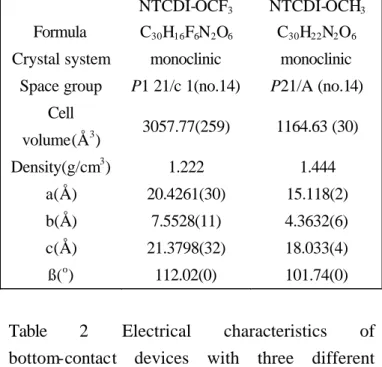
Table 1 Crystallographic data of NTCDI-OCF3
and NTCDI-OCH3
NTCDI-OCF3 NTCDI-OCH3
Formula C30H16F6N2O6 C30H22N2O6
Crystal system monoclinic monoclinic Space group P1 21/c 1(no.14) P21/A (no.14)
Cell volume(Å3) 3057.77(259) 1164.63 (30) Density(g/cm3) 1.222 1.444 a(Å ) 20.4261(30) 15.118(2) b(Å ) 7.5528(11) 4.3632(6) c(Å ) 21.3798(32) 18.033(4) ß(o) 112.02(0) 101.74(0)
Table 2 Electrical characteristics of bottom-contact devices with three different source/drain electrodes.
Source/drain electrodes (c mMobility 2 V-1 s-1)
Threshold voltage (V) On/off current ratio 1 molybdenum (Mo) 3.58×10⁻² 1.3 5.2×10⁵
2 indium tin oxide (ITO) 1.09×10⁻² 5.7 2.1×10⁵