國立交通大學
電子工程學系 電子研究所碩士班
碩士論文
應變矽金氧半導體場效電晶體
的量子模擬
Quantum Simulation of Strained Si MOSFET
研 究 生:李亨元
指導教授:陳明哲
應變矽金氧半導體場效電晶體的量子模擬
Quantum Simulation of Strained Si MOSFET
研 究 生:李亨元 Student:Hengyuan Lee
指導教授:陳明哲 Advisor:Ming Jer Chen
國立交通大學
電子工程學系 電子研究所碩士班
碩 士 論 文
A Thesis
Submitted to Department of Electronic Engineering
&Institute of Electronics
College of Electrical Engineering and Computer Science
National Chiao Tung University
in partial Fulfillment of the Requirements
for the degree of
Master of Science
in
Electronic Engineering
June 2004
Hsinchu, Taiwan, Republic of China
應變矽的金屬氧化物半導體場效電晶體
之量子模擬
研究生 : 李亨元 指導教授 : 陳明哲 博士
國立交通大學
電子工程學系 電子研究所
摘 要
在本論文中,我們建構了可以模擬應變矽的金氧半場效電晶體元件的程式, 該程式可以自我相容地解一維的 Schrödinger 和 Poisson 方程式,利用這個程 式,我們研究了一些應變矽元件的量子化特性,特別是元件在彈道傳輸下的效能 極限,以及直接穿隧的閘極漏電流。最後,我們提出並檢驗一種利用應變矽的雙 閘極元件的架構,以量產的觀點來說,這種元件比傳統的雙閘極元件更具實用價 值且有更好的元件特性。Quantum Simulation of Strained Si MOSFET
Student : Hengyuan Lee Advisor : Dr. Ming Jer Chen
Department of Electronics Engineering
& Institute of Electonics
National Chiao Tung University
Abstract
A 1-D self-consistent Schrödinger-Poisson solver for dealing with strained Si MOSFETs has been successfully constructed in this thesis. Several quantum mechanical properties of strained Si devices have also been studied, especially the ballistic performance limit and the gate direct tunneling current. Finally, a strained double gate device has been proposed and examined. This new device might provide a more practical way from the manufacturability point of view while being able to create device performance superior over traditional double gate devices.
致謝
由衷地感謝所有幫助我完成論文的人
Contents
Chinese Abstract
……….……….ⅠEnglish Abstract……….Ⅱ
Acknowledgments………..Ⅲ
Contents………..Ⅳ
List of Captions………..Ⅴ
Chapter 1 Introduction………1
Chapter 2 1-D Quantum Mechanical Simulator……….…..3
2-1 Description of the Program……….3
2-2 Simulation Results………6
Chapter 3 Quantum Simulation of the Strained Si Device………...…8
3-1 Simulation of the Strained Si Device………8
3-2 Simulation Results………...10
Chapter 4 Effect of strain on Direct Tunneling Gate Current…..…..11
4-1 Model of Direct Tunneling Current……….11
4-2 Results of Simulation………...14
4-3 Discussion………..14
5-1 Simulation of DG Device………..16
5-2 Simulation of the Strained DG Device………...16
5-3 Results of Simulation………17
5-4 Discussion………..18
Chapter 6 Conclusion……….20
List of Captions
Fig.2.1 Wave function distribution
Simulation condition: Metal gate with Φ=4.05 eV; NSUB =1*1016 cm-3
tOX = 1.65*10-9 m; Temp=300K; and VG=1.2 V
….…
23Fig.2.2 Variation of valley’s occupancy verse VG
Simulation condition: Metal gate with Φ=4.05 eV; NSUB =1*1016 cm-3;
tOX = 1.65*10-9 m; and Temp=300K
………
24Fig.2.3 Comparison of induced QINV between Si(100) and Si(110).
Simulation condition: Metal gate with Φ=4.05 eV; NSUB =8*1017 cm-3
tOX = 1.65*10-9 m; and Temp=298K
………
25Fig.2.4 Band bending as a result of body effect
Simulation condition: Metal gate with Φ=4.05 eV; NSUB =8*1017 cm-3;
tOX = 1.65*10-9 m; and Temp=298K
………
26Fig.2.5 Induced QINV under body effect.
Simulation condition: Metal gate with Φ=4.05 eV; NSUB =8*1017 cm-3;
tOX = 1.65*10-9 m; and Temp=298K
………
27Fig.3.1 The effect of biaxial tensile strss on Si band structure
………...…
28Fig.3.2 Comparison between the results from QM Simulator and Takagi [6].
Simulation condition: Metal gate with Φ=4.05 eV; NSUB =2*1016 cm-3;
tOX = 1.65*10-9 m; Temp=300K;
and QINV=1*1012cm-2
………....
29Fig.3.3 Comparison between the results from QM Simulator and Takagi [6]
Simulation condition: Metal gate with Φ=4.05eV; NSUB =2*1016 cm-3
tOX = 1.65*10-9 m; Temp=300K;
and QINV=1*1012 cm-2
………...
30Fig.3.4 Comparison between the results from QM Simulator and Takagi[7]
Simulation condition: Metal gate with Φ=4.05eV; NSUB =1*1016 cm-3
tOX = 1.65*10-9 m; Temp=300K;
and QINV=7*1012cm-2
………..….
31Fig.3.5 Comparison between the results from QM Simulator and Takagi[7]
Simulation condition: Metal gate with Φ=4.05eV; NSUB =1*1016 cm-3
tOX = 1.65*10-9 m; Temp=300K;
and QINV=7*1012 cm-2
………..….
32Fig.3.6 VG for QINV=5*1012cm-2 verses oxide thickness
tOX = 1.65*10-9 m; Temp=298K
…………..………
33Fig.4.1 Direct tunneling current from the channel
………..….…
34Fig.4.2 JG forverses VG for different Ge concentration (linear scale)
Simulation condition: Metal gate with Φ=4.05eV;NSUB =8*1017 cm-3
tOX = 1.65*10-9 m; and Temp=298K
………
35Fig.4.3 JG forverses VG for different Ge concentration (log scale)
Simulation condition: Metal gate with Φ=4.05eV; NSUB =8*1017 cm-3
tOX = 1.65*10-9 m; and Temp=298K
………
36Fig.4.4 JG,i of each subband verses VG for different Ge concentration
Simulation condition: Metal gate with Φ=4.05eV; NSUB =8*1017 cm-3
tOX = 1.65*10-9 m; and Temp=298K
………
37Fig.4.5 Comparison of JG between equilibrium and non-equilibrium
Simulation condition: Metal gate with Φ=4.05eV; NSUB =8*1017 cm-3
tOX = 1.65*10-9 m; and Temp=298K
………
38Fig.4.6 Variation of QINV vs. Ge concentration
Simulation condition: Metal gate with Φ=4.05eV; NSUB =8*1017 cm-3
tOX = 1.65*10-9 m; and Temp=298K
………
39Fig.4.7 Data of JG verse VG from AMD [11]
.………..…
40Fig.5.1 Wave function distribution
Simulation condition: Metal gate Φ1=Φ1=4.05eV; NSUB =1*1016 cm-3
tOX,1 = tOX,2 = 1.65*10-9 m; Temp=300K;
and tSi=5nm
……….…………
41Fig.5.2 Energy difference between the lowest subband of the two valley group
Simulation condition(Single gate): Metal gate with Φ=4.05eV; NSUB =1*1016
cm-3; tOX = 1.65*10-9 m; and Temp=300K
Simulation condition(Double gate):Metal gate Φ1=Φ1=4.05eV; NSUB =1*1016
cm-3; tOX,1 = tOX,2 = 1.65*10-9 m;
Temp=300K; and TSi=5nm
.……...……
42Fig 5.3. (a) Cross section view of strained Si DG device; (b) Top view of strained Si
DG device
……….……….…………
43Fig 5.4 valleys of conduction band seen from the top of device
….………
44Fig.5.5 IBALLISTIC verse VG for various Ge concentrations
Simulation condition: Metal gate Φ1=Φ1=4.05eV; NSUB =1*1016 cm-3
tOX,1 = tOX,2 = 1.65*10-9 m; Temp=300K;
and tSi=50nm
……….……….………….………
45Fig.5.6 IBALLISTIC verse VG for various Ge concentration
Simulation condition: Metal gate Φ1=Φ1=4.05eV; NSUB =1*1016 cm-3
and tSi=2nm
………....………….………
46Fig.5.7 IBALLISTIC as QINV =7*1012 cm-2 verse tSi for various Ge concentration
Simulation condition: Metal gate Φ1=Φ1=4.05eV; NSUB =1*1016 cm-3
tOX,1 = tOX,2 = 1.65*10-9 m;
and Temp=300K
………....………….……….…
47Fig.5.8 vINJ as QINV =7*1012 cm-2 verse tSi for various Ge concentration
Simulation condition: Metal gate Φ1=Φ1=4.05eV; NSUB =1*1016 cm-3
tOX,1 = tOX,2 = 1.65*10-9 m; and Temp=300K
…….…
48Fig.5.9 Electron occupancy of valley Aas QINV =7*1012 cm-2 verse tSi for various Ge
concentration
Simulation condition: Metal gate Φ1=Φ1=4.05eV; NSUB =1*1016 cm-3
tOX,1 = tOX,2 = 1.65*10-9 m; and Temp=300K
…….…
49Fig.5.10 Electron occupancy of valley Bas QINV =7*1012cm-2 verse tSi for various Ge
concentration
Simulation condition: Metal gate Φ1=Φ1=4.05eV; NSUB =1*1016 cm-3
Chapter 1
Introduction
Recently, strained MOSFET has played an important role on the way toward the nano-scale device. Because strain changes the material’s band structure, the carrier transport in the channel of the strained MOSFET has different manners than those in the unstrained one. The appropriate use of the strain can improve the device performance strikingly. Several strain technologies had been reported, which essentially can be categorized into two methods: one is substrate-induced strain and another is process strained Si (PSS). The substrate induced strain technology uses the substrate composed of the two lattice-mismatch layers. Due to this lattice mismatch, a
biaxial stress is induced in the substrate. The Si stacking on Si1-XGeX is commonly
utilized. The process strained Si employs special process technique to generate strain in the channel, including STI PSS, Cap-layer PSS, and Silicide PSS [1].
To understand the influence of strain on the electrical properties of the strained MOSFET is very important to the device modeling, and 1-D quantum simulation is necessary to conduct this issue. Because of the simple distribution of the strain,
substrate induced strain in terms of the stacking Si on Si1-XGeX has been studied
widely. In this thesis, we develop a program to quantum mechanically simulate the strained Si device on a MOS system and also examine the transport properties of interest.
In Chapter 2, SCHRED, a 1-D un-strain silicon quantum simulator from the Purdue University, which constitutes a basis for our strain version development, is introduced. The changes made in this source code to account for strain properties are detailed in Chapter 3, along with simulation results on the strained Si MOSFETs ( Si
on Si1-xGex ). In Chapter 4, we use the simulation results to study the effect of the strain on the direct tunneling gate current. In Chapter 5, a new strained silicon double gate device is proposed and examined via the developed quantum simulator. Finally, a brief conclusion is drawn in Chapter 6.
Chapter 2
1-D Quantum Mechanical Simulator
2.1 Description of the Program
As the MOSFET dimension scales down, the quantum effect is more and more important. Beside the concerned phenomena induced by the quantum effect, like poly-gate depletion and threshold voltage shift, the so-called subband engineering is also an attractive subject. To study these quantum phenomena, the self-consistent Schrödinger-Poisson simulation is needed. In this chapter, we introduce a 1-D quantum mechanical simulator developed by the group at the Purdue University [2], and another quantum mechanical simulator developed by our group. In addition, the performance limit of the device also serves as important guide during device development. In this chapter, the ballistic transport or transport without scattering is examined and linked to this limit.
SCHRED, a program developed by the group at the Purdue University [2], can quantum mechanically simulates a MOS system associated with traditional MOSFETs and double gate devices. This program solves the following equations simultaneously:
ε ρ
=
∂ ∂ 2 2 z V (Poisson equation) (1)Ψ
=
Ψ
+
Ψ
∂ ∂ −V
E
z mZ 2 2 2 2 h (Schrödinger equation) (2)For the two-fold valleys, mZ =ml, and for the fourfold valleys, mZ =mt. The
incomplete LU method. In the underlying silicon region, Poisson equation can be written in the form
Si j i j i j i depl z e N z z V ε ρ ⎥ ⎥ ⎦ ⎤ ⎢ ⎢ ⎣ ⎡ Ψ − − ∂ ∂
=
∑
, 2 , , 2 2 ) ( ) ( (3)Hereρdepl is the depletion charge density andNi,j, the 2-D carrier density in the
subband i of the valley j, is expressed as [3]
(
) (
)
{
E E kT E E qV kT}
kT m j i D j i F j i F Die
e
N
, ( , )/ ( , )/ 2ln
1
ln
1
− − −+
+
+
=
h π (4)The first term on the right-hand side of this equation is the contributions by the
carriers injected from the source, and the second term from the drain.m is the Di
density of states effective mass for subband i; for the twofold valleys, mDi =2mt, and
for the fourfold valleys, mDi =4 mtml . There are two extreme cases of Ni,j. One
is for VD =0, the equilibrium case:
{
(
)
}
kT E E kT m j i j i F Die
N
, 2 ( , )/ 2ln
1
−+
=
h π (5)Another is the non-equilibrium case at VD >>0 where the carriers from the drain are
suppressed, namely
(
)
{
E E kT}
kT m j i j i F Die
N
, ( , )/ 2ln
1
−+
=
h π (6)The shooting method are used to solve 1-D Schrödinger equation with the
boundary conditions Ψ=0 at the oxide-silicon interfaces. To describe the shooting
method, let us rewrite the time-independent Schrödinger equation in the form:
(7)
When discretized on a uniform mesh, one gets that:
(8)
Then,
1. Integrate the Schrödinger equation towards larger z from zmin with
; (9)
2. Integrate the Schrödinger equation towards smaller z starting from zmax with
; (10)
3. At the matching point zm, one matches the solutions resulting from 1 and 2, and
then renormalized theΨ ; and
(11)
When the channel length is much smaller than the mean free path of the carrier, the carrier can propagate through the channel from the source to the drain without any scatterings. This is called ballistic transport. For the ballistic limit, the injection velocity is [3]: (12) where
[ ]
x 2 1ℑ is the Fermi-Dirac integral of order one half as defined by Blakemore
[4]. mc,i is the conductivity effective mass; for the twofold valleys, mc,i =4mt and
for the fourfold valleys, mc,i =4
(
mt + ml)
2. The ballistic current can then becalculated:
=
∑
j i j i inj j i BALLISTICqN
v
I
, , , (13)2.2 Simulation Results
Fig.2.1 shows the wave functions simulated by the SCHRED. In this figure, we
see that the wave functions of the twofold valleys are larger than those of the fourfold
valleys. Because of theheavier effective mass perpendicular to the Si-oxide interface,
the twofold valleys are preferential on the electron occupancy. Fig.2.2 shows that the
(
)
[
]
⎟
⎠
⎞
⎜
⎝
⎛
=
+ − − ℑ ) 1 ln( 2 ) ( 2 1 2 EF i kBT B i F Di ci B e T k E m Tm k i injv
ε ε πelectrons mainly occupy the twofold valleys at the high gate voltage.
On the other hand, our developed quantum mechanical Simulator, the modified version of the SCHRED, can have more features. Fig.2.3 displays comparison of the
simulated Qinv between Si (110) and Si (100). For Si (110), the fourfold valleys
havemZ =0.315m0, and the twofold valleys have mZ =0.19m0 [5]. Because the
effective mass mz of the Si (110) are lighter than those of Si (100), Si (110) has
poorer ability to induce QINV.
Another new function is the simulation of the body effect. Because the quasi-Fermi level of the minority carrier is lowered down due to applied substrate bias, this gives rise to more severe band bending, as shown in Fig.2.4. The corresponding
Chapter 3
Quantum Simulation of the Strained Si Device
3.1 Simulation of the Strained Si Device
In this chapter, we show the results of quantum mechanical simulation for the strained Si MOSFET using our developed QM Simulator, and compare with those from Takagi, et al. [6,7].
MOSFET fabricated on strained Si layer pseudomorpically grown on Si1-xGex
has better device performance than that on bulk Si. Because of the lattice mismatch
between Si and Si1-xGex, the induced biaxial tensile stress on Si layer lowers the
conduction band minima of the twofold degenerate valleys relative to that of the fourfold degenerate valleys by 0.67x, and the valance band maxima of the light hole
are lower than that of the heavy hole by 0.44x + 0.219x2 - 0.142x3 [8], as shown in Fig.
3.1. For NMOS, the energy lowering of the twofold valleys makes them more dominant on electron occupancy. As a result, the lighter conductivity mass of the twofold valleys and the suppression of the intervalley scattering between the twofold and fourfold valleys enhance the device performance [7].
The following expressions concerning the dependences of material parameters on the Ge content x have been incorporated in the our simulator:
χSi = 4.05 + 0.67x [9] (14)
Eg,Si = 1.12 - 0.754x + 0.161x2 - 0.2072x3 + 0.058282x4 [10] (15)
ΔEv = Ev(heavy) – Ev(light) =0.44x + 0.219x2
– 0.142x3 (17)
where χSi is the electron affinity of the strained Si, Eg,Si is the bandgap of the
strained Si, ∆EC is the conduction band splitting between the fourfold and twofold
valleys, and ∆ is the valence band splitting between heavy hole and light hole. Ev
The following are the 3-D electron and hole density for the strained Si:
( )
(
12
)
(
)
(
12
( )
)
(
)
2 1 3 2 2 2 1 3 2 2 2 * 2 3 2 2 * 2 3 1 kT E E E h kT m kT E E h kT m F C F C Cn
=
π πℑ
−+
π πℑ
− −∆ (18))
(
)
(
2
)
(
)
(
2
2 1 2 0 2 1 2 0 1.5 2 1.5 2 1.5 2 2 5 . 1 kT E E E h kT m hl kT E E h kT m hh F V V F Vm
m
p
=
π πℑ
−+
π πℑ
−∆ − (19) Here,[ ]
x 2 1ℑ is the Fermi-Dirac integral of order one half, m*=(mlmt2)1/3, and mhh
and mhl are the effective mass of the heavy and light hole, respectively. The first
term on the right-hand side of (18) is the electron density from the twofold valleys and the second term from fourfold valley. The first term on the right-hand side of (19) is attributed to the heavy hole and the second is attributed to the light hole.
Furthermore, in the QM Simulator, we assume that the thickness of the strained layer is thick enough (typically, 60nm) to eliminate the effect of the discontinuity
between Si and Si1-XGeX. As a result, we only concern on the strained Si layer during
our simulation. If the thickness of the strained Si layer is thin, the Si1-xGex layer must
be taken into account because the Si-Si1-xGex discontinuity will influence the
simulation results, as indicated in [9].
In addition, we neglect the variation of the curvature of the energy band. It means that we assume the effective mass of the carrier is constant with the strain.
Indeed, the effective mass of the carrier is a weak function of the strain [10].
3.2 Simulation Results
In this section, the strained Si device was examined using the developed QM simulator. Fig.3.2, Fig.3.3 and Fig.3.4 show the comparisons between our results and those from Takagi’s research team. Obviously, comparable agreements are achieved. In addition, we also see that the electron occupancy of the twofold valleys increase strikingly as a result of the strain.
In Fig.3.5, the improvement of thevinjdue to the strain is apparent. More results
such as in Fig.3.6 confirm that the strained Si device is a good choice to achieve low voltage application.
Chapter 4
Effect of Strain on Direct Tunneling Gate Current
4.1 Model for Direct Tunneling Current
In this chapter, we use the previous results to study the gate direct tunneling current for the strained Si device. The gate current contributed by the carrier direct tunneling through the gate oxide is very important for the modern device. So how the Ge content of the strained device affects the direct tunneling current is of interest to us. Although the direct tunneling current can be modeled accurately by the fully quantum mechanical simulation, but it is not efficient. An analytic model for direct tunneling current has been proposed [11],[12]. This method is simple and feasible for moderate to low gate voltage regime.
According to the model [11],[12], the gate current is
∑
∑
= = j i j i j i j i Q T J J , , , , τ (20)whereJi,j is the tunneling current contributed by the carrierQi,jin the ith subband of
the jth valley, and T and τ are the tunneling probability and lifetime of that
subband, respectively.
As shown in Fig.4.1, electrons in each subband have different probabilities to tunnel through the gate oxide. The transmission probability can be approximated by
R WKB
T
T
T
=
(21)potentials, and TR is the correction factor for the reflections from the potential discontinuities. The TWKB is expressed as
(
)
⎥⎦
⎤
⎢⎣
⎡
+
=
= = − OX cat an OX OX OX g E q q E g qF m E WKBE
T
exp
4h 22
γ
'
γ
sin
1γ
'
φφ (22) where qφ
cat = qχ
c − (ESi,⊥ + ESi, ) (23) OX OX Si Si c an q E E qF t qφ
=χ
−( ,⊥ + , )− (24))
1
(
G OX E E OXE
−
=
γ
(25) ) 1 ( ' 2 g OX E E − =γ
(26)In above equations,qφcat and qφab are the barrier heights at the cathode and anode
interfaces, respectively. mOX (=0.61m0) and Eg (=9eV) are the effective mass and
bandgap of oxide, respectively. qFOXtOX is the potential drop across the oxide. ESi,⊥
and ESi,∥ are the electron energy perpendicular and parallel to the interface of Si and
oxide, respectively. χc is the discontinuity between the Si and SiO2 conduction
bands with a value of 3.15 eV.
) ( ) ( ) ( ) ( 4 ) ( ) ( ) ( ) ( 4 2 , , 2 , , 2 , , 2 , , an OX OX OX Si Si an OX OX OX Si Si cat OX Si Si cat OX Si Si q v t qF E v q v t qF E v q v E v q v E v R
T
+ ΦΦ ++ + ΦΦ ⊥ ⊥ ⊥ ⊥ ⊥ ⊥ ⊥ ⊥×
=
(27) where OX m OXv
=
γ1' 2γ (28) ⊥=
,⊥,⊥ 2 , Si Si m E Siv
(29)where vSi,⊥(ESi,⊥) and vSi,⊥(ESi,⊥+qFOXtOX) are the group velocities of the electrons incident
and leaving the oxide, respectively, and vOX(qΦcat) and vOX(qΦan) are the magnitudes of
the purely imaginary group velocity of electrons at the cathode side and anode side within the oxide, respectively.
j i,
τ , the tunneling lifetime of the electrons from the ith energy subband of the jth
valley, can be written as:
j i E j j i, , h π
τ
=
(30)Finally, the direct tunneling current contributed by the ith subband of the jth valley can be evaluated analytically:
) ( 2 1 , , , , , , ⊥ ∏= −
=
Si F Si j i j i E E E T Q j i GJ
τ (31)4.2 Results of Simulation
With the method described above and our simulation results of the strained Si, we now discuss the effect of strained Si on direct tunneling current. Fig.4.2 and Fig.4.3
reveal the relationship between gate current and VG in linear and log scale,
respectively. These figures show a certain critical gate voltage above which the gate current decreases with increasing Ge content and below which the gate current increases with increasing Ge content. Furthermore, in Fig.4.4, the gate currents contributed by twofold valleys are dominant at low gate voltage, and they increase with increasing Ge content. On the other hand, the gate currents contributed by fourfold valleys are on the order of those contributed by twofold at high gate voltage or low Ge content. Obviously, the gate currents due to fourfold valleys decrease with increasing Ge content dramatically.
Fig.4.5 shows the difference of direct tunnel current between equilibrium and non-equilibrium conditions. In this figure, we see that the non-equilibrium state of MOSFET increases the gate leakage current at high gate voltage, and this degradation is relaxed as the Ge content increases. But at low gate voltage, the non-equilibrium state exhibits a reduction in the gate leakage current, and it is less pronounced as the Ge content increases.
4.3 Discussion
We explain the above results as follows. Although the potential barrier for the electron in the twofold valleys increase with increasing Ge content, the increasing rate
of QINV at low gate voltage is much higher than that at high gate voltage, as shown in
Fig.4.6. As a result, the increasing Ge content increases the gate leakage current at low gate voltage but suppresses the gate leakage current at high gate voltage. Fig.4.7
are the experiment data from AMD [13]. Although the process conditions of this device may be different from our simulation conditions, the figure shows the same trend as the simulation.
Chapter 5
Effect of Strain on Double Gate Device
5.1 Simulation of DG Device
In this chapter, double gate device simulation, another function of Purdue’s program, is studied. A modified version of this program to study another kind of double gate strained Si device is developed.
DG device is one of the future device candidates because of its superior device performance over the single gate device. As mentioned in Chapter 2, the wave function of the fourfold valleys is larger than that of the twofold valleys. This means that the subband energy of the fourfold valleys tend to increase as the thickness of Si layer in the DG device shrinks to the comparable size of the wave function of the fourfold valleys. As a result, the energy difference in the lowest subband between the two valley groups is widening. Such quantum confinement effect makes the twofold valleys more preferential on electron occupancy, and results in the improvement of the mobility due to the suppression of the intervally scattering between the two- and fourfold valleys [12].
Fig.5.1 shows the wave function simulated by Purdue’s program for the DG device with 5nm Si layer. Because of the space confinement of the wave function, their shapes are quite different from those in Fig.2.1. Fig.5.2 shows that the energy difference between the lowest subband of the two valley groups is widening as the result of space confinement.
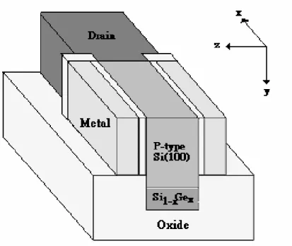
Now, we propose another kind of double gate strained Si device. The device structure is shown in Fig.5.3. Fig.5.3(a) depicts that Si(100) is pseudomorpically
grown on Si1-xGex. A narrow line with (100) sidewall surface is formed after etching
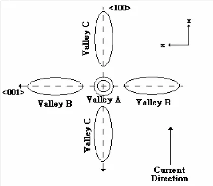
the strained Si. Then, after growing the thermally oxide on the sidewall, metal gate is formed. Finally, this device is fin-FET like device. The top view of this device is schematically shown in Fig.3.3(b). Fig.5.4 schematically displays the constant energy surface of conduction band as viewed from the top of this device, where valley A denotes the twofold degenerate valleys with the energy lowering of 0.67x by the bottom strained Si, and valley B and C denote the twofold degenerate valleys perpendicular and parallel to the interface between the oxide and Si, respectively. For
valley A,mDi =2 mtml , mc,i =4ml, for valley B,mDi =2mt,mc,i =4mt, and for
valley C, mDi =2 mtml mc,i =4mt.
Unlike the traditional DG device, the fourfold degenerate valleys are further spit into two twofold degenerate valleys. Because of the energy lowering, valley A is preferential on the electron occupancy. As a result, the intervalley scattering between any two valleys is suppressed and thereby only the intravalley scattering of the valley A needs to be concerned. Theoretically, this device should have better device performance. Unlike the subband engineering of the traditional DG device by the space confinement, this new DG device use both strain and space confinement to change the subband. Thus, this device can undergo subband engineering even for thick Si layer.
5.3 Results of Simulation
modifying Purdue’s program. Fig. 5.5 and Fig. 5.6 show simulated IBALLISTIC-VG
curves for tSi=2nm and tSi=50nm, respectively. For the thicker tSi, the inclusionof Ge
in substrate can improve the ballistic current. However, the inclusion of Ge degrades
the performance for the thinner tSi. To exploit it more, the effects of Ge content on the
ballistic current and vinj for various tSi under fixed QINV are shown in Fig. 5.7 and
Fig. 5.8, respectively. Obviously, there is a lower limit of tSi to improve device
performance by the inclusion of Ge in substrate. Fig. 5.9 and Fig.5.10 reveal the
variation of electron occupancy of valley A and valley B for various tSi under different
Ge contents.
5.4 Discussion
We explain the above results as follows. At thicker tSi, the main mechanism of
subband engineering is energy splitting of conduction band induced by strain. This energy splitting makes the valley A preferential on electron occupancy so that the
inclusion of Ge improves the device performance. However, as tSi shrinks further,
another mechanism of subband engineering, space confinement, which makes valley B preferential on electron occupancy and competitive with the previous mechanism.
As a result, the inclusion of Ge degrades the device performance at thin tSi.
Unlike the traditional DG device, which favors thin tSi, this strained silicon
device enhances the device performance at thick tSi, but degradations occur at thin tSi.
Thus, a critical thickness ofSi exist, which is found to be the thickness the space
confinement starts to influence the wave function of the inversion charge. This critical thickness is about a few nanometer (~5nm in this case), and it continues to shrink as the dopping concentration of Si increases. Such thickness is not practical in view of
manufacture. This means that the strained Si provide a more practical way to improve device performance better than traditional DG device.
Chapter 6
Conclusion
Quantum simulation of strained Si device is successful developed. The simulated
gate current via direct tunneling mechanism exhibits distinct dependencies on Ge content and gate voltage. Finally, a new strained DG device with better performance than traditional DG device is proposed and examined.
References
[1] C.Ge, et al.,“Process Strained Si CMOS Featuring 3D Strain Engineering,"IEDM, p.73, 2003.
[2] http://www.nanohub.purdue.edu.
[3] F. Assad, Z.Ren, D.Vasileska, S.Datta, and M.Lundstrom,“On the performance Limits for Si MOSFET’s:A Theoretical Study,"IEEE Transactions on Electron Device, 47, p.232, 2000.
[4] J.Blakemore,“Approximation of the Fermi-Dirac integrals, especially the function , used to describe electron density in a semiconductor," Solid State Electronics, 25, p1067, 1982.
[5] F.Stern,“Self-Consistent Results for n-Type Si Inversion Layers,"Physical Review B, 5, 4891, 1972.
[6] S. Takagi, L. Hoyt, J. Welser, and F. Gibbons,“Comparative Study of Phonon Limited Mobility of Two Dimensional Electrons in Strained and Unstrained Si Metal Oxide Semiconductor Field Effect Transitor,"Journal of Applied Physics, 80, p.1567, 1996.
[7] S. Takagi,“Re-examination of Subband Structure Engineering in Ultra Short Channel MOSFETs under Ballistic Carrier Transport,"Symposium on VLSI Technology Digest of Technical Paper, p.115, 2003.
[8] S.Galdin, P.Dollfus, Val´erie Aubry-Fortuna, P. Hesto, and H.Osten,“Band
Offset Predictions for Strained Group Ⅳ Alloys: Si1-X-YGeXCY on Si(100) and Si1-XGeX
on Si1-ZGeZ(001),"Semicond. Sci. Technol., 15, p.565, 2000.
[9] J.Goo, Q.Xiang, Y.Takamura, F.Arasnia, E.Paton, P.Besser, J.Pan, and M.Lin, “Band Offset Induced Threshold Variation in Strained Si nMOSFETs,"IEEE Electron Device Letters, 24, p.568, 2003.
[ ]
x2 1
[10] M.Reiger and P.Vogl,“Electronic-band Parameters in Strained Si1-XGeX Alloys on
Si1-ZGeZ Substrates,"Physical Review B, 48, p.14 276, 1993
[11] L.Register, E.Rosenbaum, and K.Yang,“Analytical Model for Direct Tunneling Current in Polycrystalline Si Gate Metal Oxide Semiconductor Devices,"Applied Physics Letters, 74, p.457, 1999.
[12] N.Yang, W.Henson, J.Hauser, and J.Wortman,“Modeling Study of Ultrathin Oxides Using Direct Tunneling Current and Capacitance-Voltage Measurements in MOS Devices,"IEEE Transactions on Electron Device, 46, p.1464, 1999.
[13] Q.Xiang, J.Goo, J.Pan, B.Yu, S.Ahmed, J.Zhang, and M.Lin,“Strained Si NMOS with Nickel-Silicide Metal Gate,"Symposium on VLSI Technology Digest of Technical Paper, p.101, 2003.
[14] S.Takagi, J.Koga, A.Toriumi,“Subband Structure Engineering for Performance Enhancement of Si MOSFETs,"IEDM, p.219, 1997.
0 5 10 15 20 Wa ve fu n c ti o n ( a .u .) Distance ( nm ) E1 E2 E'1 E'2
Fig.2.1 Wave function distribution Simulation condition:
Metal gate with Φ=4.05 eV; NSUB =1*1016 cm-3
0.0 0.2 0.4 0.6 0.8 1.0 1.2 35 40 45 50 55 60 65 O ccupancy ( % ) VG ( V ) Twofold Valley Fourfold Valley
Fig.2.2 Variation of valley’s occupancy verse VG
Simulation condition:
Metal gate with Φ=4.05 eV; NSUB =1*1016 cm-3;
0.0 0.2 0.4 0.6 0.8 1.0 1.2 0.0 2.0x10¹² 4.0x10¹² 6.0x10¹² 8.0x10¹² 1.0x10¹³ Q INV ( cm -2 ) VG ( V ) Si(110) Si(100)
Fig.2.3 Comparison of induced QINV between Si(100) and Si(110).
Simulation condition:
Metal gate with Φ=4.05 eV; NSUB =8*1017 cm-3
0 50 100 150 -2 -1 0 1 2 VB = 0 VB = -0.2 VB = -0.5 VB = -1 Ban d B e nd in g ( e V ) Distance ( nm )
Fig.2.4 Band bending as a result of body effect. Simulation condition:
Metal gate with Φ=4.05 eV; NSUB =8*1017 cm-3;
0.0 0.2 0.4 0.6 0.8 1.0 1.2 0.0 2.0x10¹² 4.0x10¹² 6.0x10¹² 8.0x10¹² Q IN V ( c m -2 ) VG ( V ) VB = 0 VB = -0.2 VB = -0.5 VB = -1
Fig.2.5 Induced QINV under body effect.
Simulation condition:
Metal gate with Φ=4.05 eV; NSUB =8*1017 cm-3;
Fig.3.1 The effect of biaxial tensile strss on Si band structure.
200 220 240 260 280 300 20 30 40 50 60 70 80 90 100 Occu pa ncy of 2-f o ld va lley ( % ) Temperature ( K ) Ge ( 0% ) ( QM Simulator ) Ge ( 5% ) Ge ( 10% ) Ge ( 20% ) Ge ( 0% ) ( Takagi ) Ge ( 5% ) Ge ( 10% ) Ge ( 20% )
Fig.3.2 Comparison between the results from QM Simulator and Takagi [6]. Simulation condition:
Metal gate with Φ=4.05 eV; NSUB =2*1016 cm-3;
0 5 10 15 20 0 20 40 60 80 100 120 140 100 200 300 O c cupancy of 2-fold v a lle y ( % )
Ge content of SiGe substrate ( % ) QM Simulator TAKAGI Energy diff erenc e betwe en 2-fold and 4-f o ld valley ( m e V )
Fig.3.3 Comparison between the results from QM Simulator and Takagi [6] Simulation condition:
Metal gate with Φ=4.05eV; NSUB =2*1016 cm-3
0 5 10 15 20 25 30 40 45 50 55 60 65 70 75 80 85 90 95 100 O c c upa nc y of 2-fold v alle y ( % ) Ge ( % ) 2-fold Valley QM Simulator Takagi Lowest subband QM Simulator Takagi Occu pa n cy of lo we st su b ba n d ( % )
Fig.3.4 Comparison between the results from QM Simulator and Takagi[7] Simulation condition:
Metal gate with Φ=4.05eV; NSUB =1*1016 cm-3
0 5 10 15 20 25 30 1.125x10⁷ 1.250x10⁷ 1.375x10⁷ 1.500x10⁷ 1.625x10⁷ v IN J ( cm / s ) Ge ( % ) QM Simulator current direction <100> Takagi current direction <110>
Fig.3.5 Comparison between the results from QM Simulator and Takagi[7] Simulation condition:
Metal gate with Φ=4.05eV; NSUB =1*1016 cm-3
1.2 1.4 1.6 1.8 2.0 0.40 0.45 0.50 0.55 0.60 0.65 0.70 0.75 0.80 0.85 0.90 0.95 1.00 V G ( V ) Oxide Thickness ( nm ) Si Si0.95Ge0.05 Si0.9Ge0.1 Si0.8Ge0.2 Si0.7Ge0.3
Fig.3.6 VG for QINV=5*1012cm-2 verses oxide thickness
Simulation condition:
Metal gate with Φ=4.05eV; NSUB =8*1017 cm-3
0.0 0.2 0.4 0.6 0.8 1.0 1.2 0.0 0.5 1.0 1.5 2.0 2.5 3.0 Si Si0.95Ge0.05 Si0.9Ge0.1 Si0.8Ge0.2 Si0.7Ge0.3 J G ( A / cm 2 ) VG ( V )
Fig.4.2 JG forverses VG for different Ge concentration (linear scale)
Simulation condition:
Metal gate with Φ=4.05eV;NSUB =8*1017 cm-3
0.0 0.2 0.4 0.6 0.8 1.0 1.2 1E-7 1E-6 1E-5 1E-4 1E-3 0.01 0.1 1 Si Si0.95Ge0.05 Si0.9Ge0.1 Si 0.8Ge0.2 Si0.7Ge0.3 J G ( A / c m 2 ) VG ( V )
Fig.4.3 JG forverses VG for different Ge concentration (log scale)
Simulation condition:
Metal gate with Φ=4.05eV; NSUB =8*1017 cm-3
0.0 0.2 0.4 0.6 0.8 1.0 1.2 1E-7 1E-6 1E-5 1E-4 1E-3 0.01 0.1 1 J G ( A / cm 2 ) VG ( V ) E1 E'1 ( Si ) E1 E'1 ( Si0.95Ge0.05 ) E1 E'1 ( Si0.9Ge0.1 ) E1 E'1 ( Si0.8Ge0.2 ) E1 E'1 ( Si0.7Ge0.3 )
Fig.4.4 JG,i of each subband verses VG for different Ge concentration
Simulation condition:
Metal gate with Φ=4.05eV; NSUB =8*1017 cm-3
0.0 0.2 0.4 0.6 0.8 1.0 1.2 -60 -50 -40 -30 -20 -10 0 10 20 30 Si Si0.95Ge0.05 Si0.9Ge0.1 Si0.8Ge0.2 Si0.7Ge0.3 VG ( V ) (J G, n one qu ilib ri u m - J G, eq ui libr ium ) / J G, e qui libr ium ( % )
Fig.4.5 Comparison of JG between equilibrium and non-equilibrium
Simulation condition:
Metal gate with Φ=4.05eV; NSUB =8*1017 cm-3
0.0 0.2 0.4 0.6 0.8 1.0 1.2 100 101 102 103 104 105 (Q IN V (Si 1-x Ge x ) - Q IN V (Si ))/Q INV (Si) ( % ) VG ( V ) Si0.95Ge0.05 Si0.9Ge0.1 Si0.8Ge0.2 Si 0.7Ge0.3
Fig.4.6 Variation of QINV vs. Ge concentration
Simulation condition:
Metal gate with Φ=4.05eV; NSUB =8*1017 cm-3
1 2 3 4 5 Distance ( nm ) E1 E2 E'1 E'2
Fig.5.1 Wave function distribution Simulation condition:
Metal gate Φ1=Φ1=4.05eV; NSUB =1*1016 cm-3
0.0 0.2 0.4 0.6 0.8 1.0 1.2 20 30 40 50 60 70 80 90 100 VG ( V ) Single gate
Double gate with 5nm Si layer
En
erg
y
( me
V )
Fig.5.2 Energy difference between the lowest subband of the two valley group Simulation condition(Single gate)
Metal gate with Φ=4.05eV; NSUB =1*1016 cm-3
tOX = 1.65*10-9 m; and Temp=300K
Simulation condition(Double gate)
Metal gate Φ1=Φ1=4.05eV; NSUB =1*1016 cm-3
Fig 5.3. (a) Cross section view of strained Si DG device
0.0 0.2 0.4 0.6 0.8 1.0 1.2 0.0 0.5 1.0 1.5 2.0 2.5 3.0 3.5 4.0 I BAL L IST IC ( mA / u m ) VG ( V ) Si Si0.95Ge0.05 Si0.9Ge0.1 Si 0.8Ge0.2 Si0.7Ge0.3 Si0.6Ge0.4
Fig.5.5 IBALLISTIC verse VG for various Ge concentrations
Simulation condition:
Metal gate Φ1=Φ1=4.05eV; NSUB =1*1016 cm-3
0.0 0.2 0.4 0.6 0.8 1.0 1.2 0.0 0.5 1.0 1.5 2.0 2.5 3.0 I BA L L IST IC ( mA / u m ) V G ( V ) Si Si 0.95Ge0.05 Si 0.9Ge0.1 Si 0.8Ge0.2 Si 0.7Ge0.3 Si 0.6Ge0.4
Fig.5.6 IBALLISTIC verse VG for various Ge concentration
Simulation condition:
Metal gate Φ1=Φ1=4.05eV; NSUB =1*1016 cm-3
1 10 1.3 1.4 1.5 1.6 1.7 1.8 1.9 2.0 2.1 2.2 nsub=1*1016 ( cm-3 ) QINV = 7*1012 ( cm-2 ) Si Si0.95Ge0.05 Si0.9Ge0.1 Si0.8Ge0.2 Si0.7Ge0.3 I BAL L IST IC ( mA / u m ) tSi ( nm )
Fig.5.7 IBALLISTIC as QINV =7*1012 cm-2 verse tSi for various Ge concentration
Simulation condition:
Metal gate Φ1=Φ1=4.05eV; NSUB =1*1016 cm-3
tOX,1 = tOX,2 = 1.65*10-9 m; and Temp=300K
1 10 1.250x10⁷ 1.375x10⁷ 1.500x10⁷ 1.625x10⁷ 1.750x10⁷ 1.875x10⁷ nsub=1*1016 ( cm-3 ) QINV = 7*1012 ( cm-2 ) tSi ( nm ) Si Si0.95Ge0.05 Si0.9Ge0.1 Si0.8Ge0.2 Si0.7Ge0.3 v INJ ( cm / s )
Fig.5.8 vINJ as QINV =7*1012 cm-2 verse tSi for various Ge concentration
Simulation condition:
Metal gate Φ1=Φ1=4.05eV; NSUB =1*1016 cm-3
0 10 20 30 40 50 0 20 40 60 80 100 nsub=1*1016 ( cm-3 ) QINV = 7*1012 ( cm-2 ) O c c u pa nc y ( % ) tSi ( nm ) Si Si 0.9Ge0.1 Si0.7Ge0.3
Fig.5.9 Electron occupancy of valley Aas QINV =7*1012 cm-2 verse tSi for
various Ge concentration Simulation condition:
Metal gate Φ1=Φ1=4.05eV; NSUB =1*1016 cm-3
0 10 20 30 40 50 0 20 40 60 80 100 nsub=1*1016 ( cm-3 ) Q INV = 7*10 12 ( cm-2 ) O c cu pa nc y ( % ) Si Si0.9Ge0.1 Si0.7Ge0.3 tSi ( nm )
Fig.5.10 Electron occupancy of valley Bas QINV =7*1012cm-2 verse tSi for
various Ge concentration Simulation condition:
Metal gate Φ1=Φ1=4.05eV; NSUB =1*1016 cm-3