國 立 交 通 大 學
電 信 工 程 學 系 碩 士 班
碩 士 論 文
可變超取樣率三角積分類比數位轉換器之低面
積降頻器電路設計與實現
Design and implementation of a small area decimator for
programmable oversampling ratio sigma-delta A/D converters
研 究 生:唐 江 俊
指導教授:闕 河 鳴 博士
可變超取樣率三角積分類比數位轉換器之低面積降頻器電路設計與實現
Design and implementation of a small area decimator for programmable oversampling ratio sigma-delta A/D converters
研 究 生:唐江俊 Student: Chiang-Chun Tang 指導教授:闕河鳴 博士 Advisor: Dr. Herming Chiueh
國 立 交 通 大 學 電 信 工 程 學 系 碩 士 班
碩 士 論 文
A Thesis
Submitted to Department of Communication Engineering College of Electrical and Computer Engineering
National Chiao Tung University
In Partial Fulfillment of the Requirements For the Degree of
Master of Science in Communication Engineering September 2008 Hsinchu Taiwan 西元二ΟΟ八年九月
I
積降頻器電路設計與實現
研究生: 唐江俊
指導教授:闕河鳴 博士
國立交通大學
電信工程學系碩士班
中文摘要
在很多領域,三角積分類比數位轉換器近來非常受歡迎。而三角積分類比數 位轉換器主要由類比電路(三角積分調變器)和數位電路(降頻器)所構成。然而, 數位電路部分佔據了整個三角積分類比數位轉換器的絕大多數積體電路面積。而 且對於可變超取樣率的三角積分類比數位轉換器而言,需要不同頻寬的數位濾波 器去取出所要的訊號頻段,這樣的需求也會導致額外的數位電路面積消耗。 在此,一個針對可變超取樣率三角積分類比數位轉換器的低面積降頻器被設 計與實現。而最主要的改良是在於裡頭的高階有限脈衝響應濾波器。對於調換結 構並採用多相分解的有限脈衝響應濾波器,可藉由使用摺疊和儲存元件共享技巧, 並且在此主要配合使用特別的控制電路去改變計算程序以重複使用儲存元件來 達到降低面積的目的。在此提出的電路架構,與廣泛採用的直接結構摺疊架構相 比,由於只需使用一半的儲存元件,因此可得到較小的電路面積。此外,在此提 出的架構不因節省面積而對電路的其他特性有所損傷,也就是本架構除了面積較 小外,關鍵路徑也較短,等待週期也較少並且尖峰功率消耗也較小(平均功率在 相同的水平)。 由於只需使用一半的儲存元件,本架構相對於直接結構摺疊架構而言,可使 降頻器裡的高階有限脈衝響應濾波器減少 24.6%的矽面積,進而達到整體使用四 個階段降頻器 15.8%的面積節省(對於三個階段降頻器,整體面積則可減少 20.9%)。II
Design and implementation of a small area decimator for
programmable oversampling ratio sigma-delta A/D converters
Student: Chiang-Chun Tang Advisor: Dr. Herming Chiueh
Department of Communication Engineering National Chiao Tung University
Hsinchu, Taiwan
Abstract
The sigma-delta modulation (SDM) has become a very popular analog to digital conversion technique in many fields. A sigma–delta A/D converter consists of analog circuits (sigma–delta modulator, SDM) and digital circuits (decimator). However, the silicon area of sigma-delta A/D converters is governed largely by the digital parts. Moreover, the distinct bandwidth digital lowpass filters are required to perform selecting-signal for programmable oversampling ratio SDM, which results in extra filters hardware consumption in digital part of SDM A/D converters.
The small area decimator for programmable oversampling ratio SDM A/D converters is designed and implemented. The main improvement in this thesis is focused on the high order FIR filter of decimator. Combing the folding and the storage elements sharing techniques for decimation FIR filters using polyphase decomposition in transposed-form as well as changing the computation procedures mainly to reuse storage elements by using extra control circuits, the area reduction compared with the widely used folded FIR filter architecture in direct-form is obtained due to half storage elements (registers) requirement. In addition, the extra advantages of my proposed folded decimation FIR filter architecture based on transposed-form are shorter critical path, smaller peak power (average power in the same level), and shorter latency.
As a result of half registers requirement, the 24.6% area reduction for high order (126th-order) FIR filter is obtained, which result in 15.8% area reduction for the 4-stages decimator (20.9% area reduction for 3-stages decimator).
III
Acknowledgments
首先,得感謝我的指導教授闕河鳴博士,在進實驗室之初,傳授 VLSI 相關 方面的知識,使得學生可以銜接上研究所課程,也因此最後能夠完成在 CIC 的下 線。另外,平日報告與開會時,老師也會竭力給予指導與建議以彌補學生此方面 能力的不足。除此之外,在論文撰寫期間,老師也花了很多時間精力在協助學生 修改論文並提供許多寶貴意見與硬體設備上的支援,使得此論文得以順利的完成, 在此由衷感謝。 其次,非常感謝蘇韋力學長、張紹宣學長、蔡佐昇學長,平日在學業上的解 惑,幫助本人克服此不熟悉的領域(晶片設計)。 另外,在此枯燥煩悶的研究生活裡,幸虧有呂秉勳、蘇品翰、游凱迪、賴明 君、吳春慧、林信太、吳俊誼、劉嘉儀、林順華學長還有玄奘朋友們的陪伴,使 得我三年的研究生活不感到孤單,謝謝你們。 最後,我得感謝我的父母,無論是精神上或是經濟上都給予最大的支持,使 得我無後顧之憂得以盡心完成學業,也由於父母的支持,才讓我能有動力完成這 份論文。 唐江俊 Sep. 2008IV
Contents
中文摘要 I English Abstract II Acknowledgments III Contents IV List of Tables VIList of Figures VIII
List of Abbreviations and Symbols XIII
Chapter1 Introduction 1
1.1 Motivation 2
1.2 Fundamentals 2
1.2.1 Sampling Theorem 3
1.2.2 Principle of Sigma-Delta A/D Converter 5
1.2.3 Decimator 15
1.3 A Brief Introduction of Proposed Solution 22
1.4 Thesis Organization 23
Chapter2 Decimator Architecture and Design 25
2.1 Considerations about SDM Quantization Noise 25
2.2 Decimator Architecture 27
2.3 First Decimation Stage 29
2.3.1 Introduction to Modified Comb Filters 31
2.3.2 Stage1 Design 35
2.4 Decimation FIR Filters 39
2.4.1 Stage2 Design 40
2.4.2 Stage3 Design 43
2.5 Compensation FIR Filter 46
2.5.1 Stage4 Design 48
2.6 Specification Summary 49
Chapter3 Decimator Implementation 53
3.1 Implementation and Verification Flow 53
3.2 Previous Work Comparison 56
V
3.4 Clock Divider Circuit 74
3.5 The First Decimation Stage: Comb Filter 75
3.5.1 Gain Control 75
3.5.2 Pipelined Comb Filter 76
3.6 Proposed Circuit for FIR Filters 77
3.7 Comparisons 84
3.8 Implementation Results 90
3.8.1 Pad Assignment 92
3.9 Decimator Simulation Result 93
3.9.1 OSR=128 93
3.9.2 OSR=64 95
3.10 Specification Table 97
3.11 Paper Comparison 98
Chapter4 Testing and Measurement Results 99
4.1 Introduction to Digital IC Testing using Agilent 93000 in CIC 99
4.2 Shmoo Plot 104 4.2.1 OSR=128 104 4.2.2 OSR=64 107 4.3 Timing Diagram 110 4.4 Measured Power 111 4.5 CHIP Summary 112 Chapter5 Conclusions 114
Appendix A: Filter Coefficients 116
Appendix B: Test-Patterns for Agilent 93000 119
VI
List of Tables
Table 1.1 Ideal Peak SNR with 1-bit quantizer (N=1) 14
Table 2.1 Optimized rotated angle α represented by q, which is independent to fb 34
Table 2.2 Ideal in-band quantization noise power 36
Table 2.3 Aliasing power using comb filter and MCFs with different order for 1-bit 4th-order SDM, OSR=128 and OSR=64 (calculating in Matlab) 36 Table 2.4 Quantization noise power which cannot be remove by latter filter 40 Table 2.5 Aliasing power2 with different stop-band attenuation 41 Table 2.6 Quantization noise power in in-band after 2nd decimation stage 44 Table 2.7 Aliasing power3 with different stop-band attenuation (Rs)
, given a narrow transition-band (0.02). 44
Table 2.8 FIR orders and aliasing power3 with different widths of transition-band 44 Table 2.9 Pass-band ripple with different order of compensation filter for
decimation ratio=128 48
Table 2.10 Pass-band ripple with different order of compensation filter for
decimation ratio=64 48
Table 2.11 Summary of decimation filter specifications 49
Table 2.12 Aliasing power, remaining quantization noise power and obtained SNR
at each stage for OSR=128 50
Table 2.13 Aliasing power, remaining quantization noise power and obtained SNR
at each stage for OSR=64 50
Table 3.1 required word-length for these two structures 57
Table 3.2 The computation of each cycle in Figure 3.22(a) 81 Table 3.3 The algorithmic operations of proposed folded architecture is equivalent
to the unfolded decimation FIR filter in transposed-form using polyphase 82 Table 3.4 Comparison of decimator
using the described implementations of FIR filter 84 Table 3.5 Detail area comparison of decimator
using the described implementations of FIR filters 85 Table 3.6 Area normalized to direct-form folding (27-bits word-length) 85
Table 3.7 Detail Power Comparison 86
Table 3.8 Detail area comparison with 16-bits word-length 87 Table 3.9 Area normalized to direct-form folding (16-bits word-length) 87 Table 3.10 Detail power comparison using 16-bits word-length 88
Table 3.11 Pad and silicon area of the chip (decimator) 91
VII
Table 4.2 Measured power consumption 111
Table 4.3 Chip summary 112
Table A.1 Coefficients of the 2nd-stage FIR filter 116
Table A.2 Coefficients of the 3rd-stage FIR filter 116
VIII
List of Figures
Figure 1.1 (a) Continuous-time signal xc(t)
(b) its (continuous-time) Fourier transform Xc(f) 3 Figure 1.2 (a) Continuous-time to discrete-time conversion system
(b) periodic impulse train s(t) 3
Figure 1.3 (a) Sampled signal xs(t)
(b) its (continuous-time) Fourier transform Xs(f) 4 Figure 1.4 (a) Discrete-time sequence x[n]
(b) its discrete-time Fourier transform (DTFT) X(fd) 5
Figure 1.5 Transfer Curve of a quantizer 6
Figure 1.6 Power spectral density of signal and quantization noise
(a) Nyquist sampling (b) oversampling 8
Figure 1.7 Power spectral density of signal and quantization noise (a) Nyquist sampling
(b) oversampling and removing out-of-band quantization noise 8 Figure 1.8 Power spectral density of signal and quantization noise
after down-sampling 9
Figure 1.9 Procedure to obtain Nyquist rate high SNR signal 9
Figure 1.10 Decimator components 10
Figure 1.11 Power spectral density of signal and quantization noise
for noise-shaping 11
Figure 1.12 Power spectral density of signal and quantization noise
for oversampling and noise-shaping 12
Figure 1.13 Ideal noise transfer function (NTF) for different order SDM 15 Figure 1.14 (a) Decimator components
(b) Behavior of decimator for SDM in time domain 16 (c) Behavior of decimator for SDM in frequency domain 17 Figure 1.15 (a) Aliasing-band of signal
(b) cut-off-band of low-pass filter designed to prevent aliasing 18
Figure 1.16 Downsampler 19
Figure 1.17 (a) X(f)
(b) Xd(f) aliased by other copies of X(f/D-i/D) (i.e., i=1,2,3), D=4 19
Figure 1.18 The bands in aliasing band [0.5/D, 0.5]
IX
the trace-back process in this demonstration. 20
Figure 1.20 There are D-1 folding-bands for down-sampling D. 21
Figure 1.21 Filter specifications for low-pass filter 22
Figure 2.1 (a) frequency over [-0.5, 0.5] (b) frequency over [0, 1] (c) frequency over [0,0.5].
The signals represented by these figure are the same. 26
Figure 2.2 Decimator architectures 28
Figure 2.3 For 1-bit 4th-order OSR-128 SDM, decimator architectures in terms of SNR, number of required multiplication operations per second and
pass-band ripple are shown. 29
Figure 2.4 zero-pole plot for 5th-order comb filter with D=32
(5*32 zeros around unit circle, 5 poles in z=1 and the other poles in z=0) 30 Figure 2.5 Magnitude frequency response of 5th-order comb filter with D=32
(half periodic spectrum have been depicted,
so there are D/2=16 notches in spectrum) 31
Figure 2.6 zero-pole plot of (a) 1st-order comb filter
(b) counterclockwise rotated of 1st-order comb filter (c) clockwise rotated of 1st-order comb filter
(d) 3rd-order modified comb filter, with D=4. 33
Figure 2.7 Magnitude response (dB) of 3rd-order modified comb filter (MCF3)
with D=4 34
Figure 2.8 Magnitude responses of Comb3 and MCF3 in folding-band
The MCF3 can suppress more quantization noise power in folding-band. 35 Figure 2.9 The flow for quantization noise power spectral density of SDM
in first decimation stage 37
Figure 2.10 Quantization noise power spectral density of 1-bit 4th-order
sigma-delta modulator 38
Figure 2.11 First decimation filter (comb filter with D=32 for the left graph and 16 for the right graph, respectively). Folding-bands of these two
magnitude response are both in the notch position, each D-1
folding-bands 38
Figure 2.12 Quantization noise PSD after first decimation filter 38
Figure 2.13 Quantization noise PSD after down-sampling 39
Figure 2.14 Folding-band for 2nd decimation stage 40
Figure 2.15 Flow for quantization noise power spectral density
X
Figure 2.16 Quantization noise PSD after down-sampling1 41
Figure 2.17 Magnitude response of 2nd stage decimation filter (FIR1)
with quantized coefficients 42
Figure 2.18 Quantization noise PSD after 2nd decimation filter 42 Figure 2.19 Quantization noise PSD after down-sampling 2 43
Figure 2.20 Folding-band of 3rd decimation stage 43
Figure 2.21 Flow for quantization noise power spectral density
in 3rd decimation stage 45
Figure 2.22 Quantization noise PSD after down-sampling 2 45 Figure 2.23 Magnitude response of 3rd stage decimation filter (FIR2)
with quantized coefficients 45
Figure 2.24 Quantization noise PSD after 3rd decimation filter 46
Figure 2.25 Quantization noise PSD after down-sampling 46
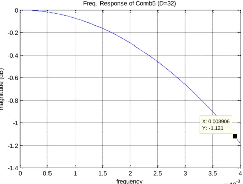
Figure 2.26 Pass-band drop of comb filter with D=32 for OSR=128
(fb=0.5/OSR=3.90625e-3) 47
Figure 2.27 Pass-band drop of comb filter with D=16 for OSR=64
(fb=0.5/OSR=7.8125e-3) 47
Figure 2.28 Magnitude response of compensation filter in the 4th stage 49
Figure 2.29 Magnitude response of each stage 50
Figure 2.30 Quantization noise power spectral density (dB) of
1-bit 4th-order SDM 51
Figure 2.31 Magnitude response of equivalent single stage low-pass filter
for decimation ratio 128 52
Figure 2.32 Magnitude response of equivalent single stage low-pass filter
for decimation ratio 64 52
Figure 3.1 The cell-based implementation flow of digital IC 54 Figure 3.2 Simulation and verification procedures of decimator 55 Figure 3.3 Commutative rule: the system in (a) is equivalent to the system in (b). 56 Figure 3.4 Comparison of recursive and non-recursive algorithm of comb filter in
terms power, area, speed, power speed product 58
Figure 3.5 System A is equivalent to system B (polyphase decomposition;
efficient implementation for FIR filter followed by down-sampling). 61 Figure 3.6 Efficient implementation of decimation FIR filter with M=2 62 Figure 3.7 Decimation FIR filter (126th-order) with polyphase decomposition
in direct-form 63
Figure 3.8 The meaning of switched arrow where f denotes the sampling rate 64 Figure 3.9 The folded architecture of FIR filter with polyphase decomposition
XI
Figure 3.11 The values stored in storage elements 68
Figure 3.12 Folded architecture of k-tap FIR filter in transposed-form without polyphase decomposition (i.e. no down-sampling)
(for linear-phase, the feature of FIR filter coefficients: hn=hk-1-n) 70 Figure 3.13 Corresponding unfolded FIR filter in transposed form 70 Figure 3.14 Folded architecture of decimation FIR filter
using polyphase decomposition 72
Figure 3.15 Block diagram of overall decimator system 73
Figure 3.16 Circuit of clock divider by 2 74
Figure 3.17 Timing diagram for the circuit of clock divider by 2 74
Figure 3.18 Components of first decimation stage 75
Figure 3.19 Pipelined comb filter
(only integrators part needed to be pipelined due to its critical timing) 76
Figure 3.20 Retiming to reduce the registers usage 77
Figure 3.21 Implementation of first decimation stage 77
Figure 3.22 (a) Proposed folded architecture of decimation FIR filter based on transposed-form using polyphase decomposition
(b) the unfolded one 79
(c) Timing diagram of my proposed architecture 80
Figure 3.23 Parts of control circuits 83
Figure 3.24 Trade-off between unfolded and folded FIR Filter 89 Figure 3.25 Trade-off between the three folded architectures 90
Figure 3.26 Layout of decimator 91
Figure 3.27 Pad assignment 92
Figure 3.28 The post-layout gate-level simulation and verification flow
for decimator 93
Figure 3.29 Post-layout gate-level simulation result with decimation factor=128
at nWave of workstation 94
Figure 3.30 Verification in time domain and frequency domain
for decimation ratio 128 using Matlab 94
Figure 3.31 Post-layout gate-level simulation result with decimation factor=64
at nWave of workstation 96
Figure 3.32 Verification in time domain and frequency domain
for decimation ratio 64 using Matlab 96
Figure 4.1 P600 test system of Agilent 93000 SoC Series 100
XII
Figure 4.3 (a) DUT board on test-head of Agilent 93000 101 (b) chip in socket of DUT board
(c) the reverse-side of DUT board wired the core-power and io-power of the chip to power-supplies pins
(d) Software (SmarTest) used to manipulate the Agilent 93000
in workstation (unix-system) 102
Figure 4.4 Test-pattern for Agilent 93000 composed of drive vector (input of DUT)
and expected vector (expected output of DUT) 103
Figure 4.5 Flow of function test 103
Figure 4.6 Shmoo plot (128) 104
Figure 4.7 The spectrums for drive vector (IN) and expected vector (OUT),
decimation factor 128 105
Figure 4.8 Spectrums of decimator input and output over the frequency range
[100Hz 25.6MHz] (128) 106
Figure 4.9 Shmoo plot (64) 107
Figure 4.10 The spectrums for drive vector (IN) and expected vector (OUT),
decimation factor 64 108
Figure 4.11 Spectrums of decimator input and output over the frequency range
[100Hz 12.8MHz] (64) 109
Figure 4.12 Timing diagram (decimation ratio 128) plotted by Agilent 93000 110 Figure 4.13 Timing diagram (decimation ratio 64) plotted by Agilent 93000 111 Figure B.1 Corresponding waveforms of state characters of signals in my design 119
Figure B.2 Parts of test vectors for SDM with OSR 128 120
Figure B.3 Corresponding post-layout-simulation of parts’ test vectors
for SDM with OSR 128 121
Figure B.4 The corresponding timing diagram measured by Agilent 93000 (128) 122 Figure B.5 The corresponding post-layout-simulation (128) 122
Figure B.6 Parts of test vectors for SDM with OSR 64 123
Figure B.7 Corresponding post-layout-simulation of parts’ test vectors
for SDM with OSR 64 124
Figure B.8 The corresponding timing diagram measured by Agilent 93000 (64) 125 Figure B.9 The corresponding post-layout-simulation (64) 125
XIII
ADC Analog-to-Digital Converter
APR Auto Place&Route
AWG Arbitrary-Waveform-Generator
BW Band-Width
CIC Chip Implementation Center
CMOS Complementary Metal-Oxide Semiconductor
CTFT Continuous Time Fourier Transform
DAC Digital-to-Analog Converter
DFT Discrete Fourier Transform
DPS Device-Power Supplies
DSP Discrete-time Signal Processing
DTFT Discrete-time Fourier Transform
DUT Device Under Test
ENOB Effective Number Of Bits
FFT Fast Fourier Transform
FIR Finite Impulse Response
Fp End Frequency of Pass-band
Fs Beginning Frequency of Stop-band
fs Sampling frequency
IIR Infinite Impulse Response
LSB Least Significant Bit
OSR Over-Sampling Ratio
PCB Printed Circuit Board
PSD Power Spectral Density
Rp Maximum Pass-band Ripple
Rs Minimum Stop-band Attenuation
SDM Sigma-Delta Modulator
SNR Signal-to-Noise Ratio
Chapter 1: Introduction ~ 1 ~ __________________________________
CHAPTER
1
__________________________________Introduction
With the advance in VLSI technology, sigma-delta modulation (SDM) has become a very popular analog to digital conversion technique in many fields, such as voice, audio, telecommunication (wireless: 3G and 4G mobile terminals; wire-line: xDSL moderns ), etc. Since high resolution of sigma-delta A/D converters can be achieved by techniques, over-sampling and noise-shaping, even using 1-bit quantizer in the A/D converter [1]. That relieves the analog circuit design, which means that no accurate multi-bit quantizer is needed, like 16-bit or 24-bit quantizer, and a wide transition-band of anti-aliasing analog filter can be accepted due to over-sampling (imply that analog filter is easy to design and its cost is low). However, it needs digital hardware to finish the remaining A/D conversion jobs, which are removing out-of-band quantization noise, converting 1-bit to multi-bit (such as 16-bit) and down-sampling to Nyquist rate. In other words, the sigma-delta is one kind of A/D conversion method which moves the high resolution difficulty encountered in analog part to digital part. So the high resolution sigma-delta A/D converters are more attractive and applicable than other A/D conversion methods as the VLSI technology advances.
~ 2 ~
In addition, wireless communication devices demand multi-standard operation, which means that different signal bandwidth and different dynamic range requirements are needed. And a sigma-delta A/D converter is a best choice to perform baseband channel select filtering in digital domain as well as to meet these different bandwidth and dynamic range requirements by changing sampling rate and selecting over-sampling ratio (OSR), respectively.
1.1 Motivation
A sigma–delta A/D converter consists of analog circuits (sigma–delta modulator, SDM) and digital circuits (decimator, namely decimation filter and down-sample circuit). Although the resolution of the sigma-delta A/D converter is typically determined by the analog modulators, silicon area of the sigma-delta A/D converter is governed largely by the digital decimation filters. For example, the digital part of sigma-delta A/D converter governs 78% area in [2]. So it is more important to reduce the not crucial part’s silicon area, namely digital part’s silicon area.
Furthermore, for a programmable OSR sigma-delta A/D converter, a decimation filter with programmable decimation ratios is needed. That means different low-pass filters are needed to obtain different spectrums for down-sampling. Therefore, digital hardware would increase by several times. As a result of that, digital parts of the sigma-delta A/D converter would govern more silicon area percentage.
For cost concerns, the silicon area of the sigma-delta A/D converter must be minimized. Of course, the silicon area of the digital part (decimator) is main part needed to be improved, which dominates the silicon area of whole A/D converter. And typically, decimator consists of comb filter and several stages finite-impulse-response filters (FIR filters). The high order FIR would dominate the decimator silicon area. For instance, area of high order FIR filter would govern 80% decimator area in a three stages decimator case (comb, 18th-order FIR, and 126th-order FIR).
Now, it is quite obvious that area of high order FIR filter is the main part this thesis wants to improve as well as to keep the programmable decimation ratio decimator area overhead minimum.
1.2 Fundamentals
This section would introduce the concepts of signal processing and show the meaning of signal processing terminologies, such as sampling theorem, aliasing, folding-band, etc. Also, principle of sigma-delta A/D converter would be described.
Chapter 1: Introduction
~ 3 ~
1.2.1 Sampling Theorem
[3]Let xc(t) be a band-limited continuous-time signal with
Xc(f)=0 for |f|≥fB
Xc(f) is continuous-time Fourier transform of xc(t). And xc(t) and Xc(f) are shown
in Figure 1.1(a) and Figure1.1(b), respectively.
t f fB xc(t) X c(f) 1 -fB 0 0 (a) (b)
Figure 1.1 (a) Continuous-time signal xc(t) (b) its (continuous-time) Fourier transform
Xc(f)
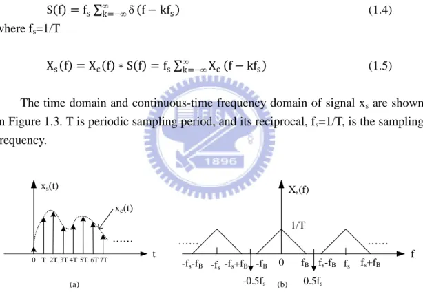
It is convenient to understand the continuous-time to discrete-time conversion mathematically in two stages depicted in Figure 1.2, namely sampling process [3].
x xs(t) Conversion from impulse train to discrete-time sequence xc(t) s(t) x[n]=xc(nT) (a) t s(t) 0 T 2T3T 4T5T6T 7T …… …… (b)
Figure 1.2 (a) Continuous-time to discrete-time conversion system (b) periodic impulse train s(t)
~ 4 ~
s t = ∞ δ t − nT
𝑛=−∞ (1.1)
xs t = xc t s t = xc t ∞𝑛=−∞δ t − nT (1.2)
xs t = ∞𝑛=−∞xc nT δ t − nT (1.3)
And, continuous-time Fourier transform of s(t) and xs(t) are S(f) and Xs(f),
respectively.
S f = fs ∞k=−∞δ f − kfs (1.4)
where fs=1/T
Xs f = Xc f ∗ S f = fs ∞k=−∞Xc f − kfs (1.5)
The time domain and continuous-time frequency domain of signal xs are shown
in Figure 1.3. T is periodic sampling period, and its reciprocal, fs=1/T, is the sampling
frequency. t f fB xs(t) Xs(f) 1/T fs -fs -fB fs-fB 0.5fs -fs+fB -0.5fs 0 0 T 2T xc(t) 5T 3T 4T 6T 7T (a) (b) fs+fB -fs-fB …… …… ……
Figure 1.3 (a) Sampled signal xs(t) (b) its (continuous-time) Fourier transform Xs(f)
Xs(f) consists of periodically repeated copies of Xc(f) ,which are shifted by
integer multiples of sampling frequency. It is obvious that when fs-fB > fB
the replicas of Xc(f) do not overlap, which means the signal xc(t) could be recovered
from xs(t) with an ideal low-pass filter. The minimum sampling rate for non-overlap
Chapter 1: Introduction
~ 5 ~
For discrete-time signal processing, discrete-time sequence, x[n], is a better representation for computer and digital system design (including digital filter). Also, the discrete-time Fourier transform would be introduce, which is suitable for discrete-time signal. And its relation is shown below in Figure 1.4.
t fd fB/fs x[n] X(f d) 1/T 1 -1 -fB/fs 1-fB/fs 0.5 -1+fB/fs -0.5 0 0 1 2 xc(t) 5 3 4 6 7 (a) (b) -1-fB/fs 1+fB/fs …… …… ……
Figure 1.4 (a) Discrete-time sequence x[n] (b) its discrete-time Fourier transform (DTFT) X(fd)
fd =
f fs
x n = xc 𝑛𝑇 − ∞ < 𝑛 < ∞ 𝑤ℎ𝑒𝑟𝑒 𝑛 𝑖𝑠 𝑎𝑛 𝑖𝑛𝑡𝑒𝑔𝑒𝑟.
fd is digital frequency for discrete-time sequences, which means frequency for
discrete-time Fourier transform. fd is frequency normalized to sampling frequency, fs.
Because there is no time information on the discrete-time sequence x[n], there is no frequency information (Hz) for discrete-time Fourier transform (only normalized frequency between -0.5~0.5). And 1 in fd represents the sampling frequency.
For conveniences, the digital frequency fd will be used in following chapters to
design and illustrate digital filter spectrum. And if x[n] is a real number sequence, the X(fd) will be even function, which means that only frequency range between 0 and 0.5
needs to be depicted in spectrum graphs.
1.2.2 Principle of Sigma-Delta A/D Converter
[1]Previous section introduces the continuous-time to discrete-time conversion, namely sampling. However, the analog to digital (A/D) conversion consists of sampling and quantization, which are discrete in time and amplitude respectively.
It is called a quantization process that an infinite number of input amplitude values are mapped into finite number of output amplitude values, which is shown in Figure 1.5.
~ 6 ~
Δ
Input x[n] output y[n]V
-V
Figure 1.5 Transfer Curve of a quantizer
For a N-bit quantizer with quantization levels L=2N, quantization error between output and input do not exceed half a least significant bit (LSB).
Δ=2V/(L-1)= LSB −∆/2 ≤ e ≤ ∆/2 e is quantization error, i.e., e=output-input. That implies
y[n]=x[n]+e[n] (1.6)
In order to simplify the analysis of quantization error, some assumptions about noise process due to quantization are made:
The error sequence, e[n], is a sample sequence of the stationary random process. The error sequence, e[n], is uncorrelated with the input.
The probability density function of random process e[n] is uniform distributed over [−∆/2, ∆/2].
The random variables of random process e[n] are uncorrelated, i.e., the random process e[n] is a white noise process, which means that the power spectrum density of e[n] is uniform distributed over [-0.5,0.5] in fd.
These assumptions are reasonable when N is large, quantizer is not overloaded, and the successive signal values are not extremely correlated [1].
Chapter 1: Introduction
~ 7 ~
example, the power of e[n] is its variance σe2
σe2 = ∆122 = 2V L−1 2 12 = 2V 2N −1 2 12 ≅ 2V 2N 2 12 (1.7)
And then, the signal to noise ration, SNR is SNR = 10 log σx2
σe2 (1.8)
where σx2 is signal power. For sinusoidal input, amplitude is V, and then signal power
σx2 is V2
/2.
SNR = 10 log σx2
σe2 = 6.02𝑁 + 1.76 (𝑑𝐵) (1.9)
The meaning of this Equation 1.9 is that SNR would increase about 6dB when one bit increased in N. However, when N is larger than 10-bit, the precision of quantizer is hard to maintain due to the very small ∆ (LSB). For example, 10-bit quantizer means that the quantization levels is L=210, which implies that Δ=2V/(L-1)=2*1.8/(210
-1)=3.52x10⁻³ (Volt) for V=1.8 (Volt). Any component mismatches and process variation would cause quantization error greater than ∆, which means the N-bit resolution could not be obtain.
To obtain high resolution, two techniques, oversampling and noise-shaping, can be used to overcome the difficulties encountered in above situations.
Oversampling
Oversampling means that signal samples are acquired from analog signal waveform much faster than Nyquist rate. For quantization noise assumptions, the noise would uniform distributed over [-0.5, 0.5] in fd. And then the technique,
oversampling, would change the distribution of signal power spectral density in fd.
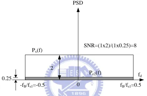
For example, the signal power spectral density (PSD) would distributed over [-0.125, 0.125] for over-sampling-ratio (OSR=4), which is different from signal PSD distributed over [-0.5, 0.5] for Nyquist rate sampling. Also the magnitude of signal PSD would change according to sampling frequency (see section 1.2.1, 1/T in Figure 1.4), which makes the signal power identical with different sampling frequency or OSR. The PSD of signal and quantization noise with different sampling frequency are shown in Figure 1.6.
~ 8 ~ 0 fB/fs1=0.5 -fB/fs1=-0.5 fd fd fB/fs2=0.125 -fB/fs2=-0.125 0.5 -0.5 PSD PSD Px(f) Pe(f) Pxo(f) Pe(f) OSR=4 fs2= 4*fs1 fs1= Nyquist rate =2fB (a) (b) 0 SNR=(1x2)/(1x1)=2 1 2 SNR=(0.25x8)/(1x1)=2 8 1
Figure 1.6 Power spectral density of signal and quantization noise (a) Nyquist sampling (b) oversampling
Before further digital signal processing, the SNR of Figure 1.6(a) and Figure 1.6(b) are the same. However, oversampling makes the distribution of signal PSD different. For OSR=4, the signal PSD is distributed over [-0.125, 0.125], which means that a digital low-pass filter could be utilized to remove the quantization noise out of the range [-0.125, 0.125] and higher SNR can be obtained. The improved SNR is illustrated in Figure 1.7. 0 fB/fs1=0.5 -fB/fs1=-0.5 fd fd fB/fs2=0.125 -fB/fs2=-0.125 0.5 -0.5 PSD PSD Px(f) Pe(f) Pxo(f) Pe1(f) OSR=4 fs2= 4*fs1 fs1= Nyquist rate =2fB (a) (b) 0 SNR=(1x2)/(1x1)=2 2 1 SNR=(0.25x8)/(0.25x1)=8 8 1
Figure 1.7 Power spectral density of signal and quantization noise
Chapter 1: Introduction
~ 9 ~
The improved SNR by oversampling= the original SNR * OSR or
The improved SNR by oversampling= the original SNR + 3.01*log2OSR (dB)
Because no signal information on the frequency [-0.5, -0.125] and [0.125, 0.5], that means the lower sampling frequency, such as Nyquist rate (2*fB), can be used to
represent the signal well. And then the PSD is changed as Figure 1.8
fd fB/fs1=0.5 -fB/fs1=-0.5 PSD Px(f) Pe2(f) 0 SNR=(1x2)/(1x0.25)=8 2 0.25
Figure 1.8 Power spectral density of signal and quantization noise after down-sampling
Now, Figure 1.9 (from Figure 1.6(b) to Figure 1.7(b) and then to Figure 1.8) demonstrates the function of the decimator, which is composed of digital low-pass filter and downsampler (circuit of lowering the sampling rate) shown in Figure1.10.
fd fB/fs1=0.5 -fB/fs1=-0.5 PSD Px(f) Pe2(f) 0 SNR=(1x2)/(1x0.25)=8 2 0.25 fd fB/fs2=0.125 -fB/fs2=-0.125 0.5 -0.5 PSD Pxo(f) Pe1(f) 0 SNR=(0.25x8)/(0.25x1)=8 8 1 fd fB/fs2=0.125 -fB/fs2=-0.125 0.5 -0.5 PSD Pxo(f) Pe(f) 0 SNR=(0.25x8)/(1x1)=2 8 1
Digital low-pass filter Downsampler
fs1=fs2/4
~ 10 ~
Ideal Digital Low-Pass Filter
Downsampler
↓
Decimator
Figure 1.10 Decimator components
Noise Shaping
In above quantization noise assumptions, the quantization noise PSD is uniform distributed over [-0.5, 0.5] in fd. And noise-shaping is a modulation technique to
change the shape of the quantization noise PSD.
Now, for easily understanding, z domain representations of signal would be introduced. Z-transform is a best representation for discrete-time signal and systems as Laplace transform for continuous-time. Also z-transform has a similar relationship to the corresponding Fourier transform, which is z = ej2πfd. For conveniences, the z-transform of input (x[n]), output (y[n]), and quantization error (e[n]) would be used and relationship of A/D could be expressed as follows:
Y(z) =X(z)+E(z) (1.10)
where Y(z), X(z), and E(z) are z-transform of y[n], x[n], and e[z], respectively.
Generally, some modulation could be used during the A/D conversion, so the relationship between output, input, and quantization error could be rewrite as follow:
Y(z) =X(z)Hx(z)+E(z)He(z) (1.11)
Noise-shaping is a technique to change the distribution of quantization noise PSD over [-0.5, 0.5] in fd as Figure 1.11.
Chapter 1: Introduction ~ 11 ~ 0 fB/fs1=0.5 -fB/fs1=-0.5 fd PSD Px(f) Pes(f) 2
Figure 1.11 Power spectral density of signal and quantization noise for noise-shaping
Sigma-Delta A/D converters
Sigma-delta A/D converters is based on two techniques, oversampling and noise-shaping. Combining oversampling and noise shaping, sigma-delta A/D converters could obtain a very high resolution (SNR). The general form for kth-order sigma-delta modulator could be written as:
Y(z) =X(z)z-k + E(z)(1-z-1)k (1.12)
Hx(z)= z-k (1.13)
He(z)= (1-z-1)k (1.14)
Now the peak SNR for sinusoidal signal can be derived according to quantization bit N, OSR, and kth-order SDM noise transfer function: (f represents normalized frequency, fd, for following analysis)
z = ej2πf , the relationship between z domain and frequency domain
(1.15) Hx(f)=e−j2πkf (1.16) He(f)= 1 − e−j2πf k = e−jπf ejπf+ e−jπf k = 2ke−jkπfsink πf (1.17)
~ 12 ~
For Y(f)=X(f)H(f) in frequency domain, i.e., y[n]=x[n]*h[n] in time domain, and then the relationship of the power spectral density (PSD) between input, output, transfer function is Py f = Px f H f 2 . So,
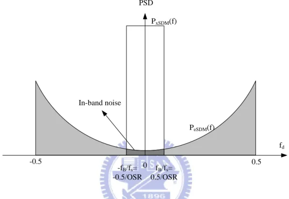
0 0.5 -0.5 fd PSD PxSDM(f) PeSDM(f) -fB/fs= -0.5/OSR fB/fs= 0.5/OSR In-band noise
Figure 1.12 Power spectral density of signal and quantization noise for oversampling and noise-shaping PxSDM f = Px f Hx f 2 = Px f e−j2πkf 2 = Px f (1.18) PeSDM f = Pe f He f 2 = Pe f 1 − e−j2πf k 2 = Pe f 2ke−jkπfsink πf 2 = Pe f 22ksin2k πf (1.19)
Chapter 1: Introduction
~ 13 ~
PxSDM(f): Signal PSD of SDM over [-0.5/OSR, 0.5/OSR] in f, i.e. fd.
PeSDM(f): Quantization noise PSD of SDM over [-0.5, 0.5] in f, i.e. fd
Px f = σx 2 1 OSR = V2 2 OSR (1.20) Pe f = ∆2 12 1 = ( 2V 2N −1) 2 12 ≅ (2V 2N) 2 12 (1.21)
Signal power is still the same PWRsignal = σx2 = V
2 2 OSR df = 0.5 OSR −0.5 OSR V2 2
As a result of that signal spectrum is distributed over [-fB/fs, fB/fs] (or [-0.5/OSR,
0.5/OSR]). So inband quantization noise power QNin-band :
QNin −band = Pe f He f 2 df 0.5 OSR −0.5 OSR =( 2V 2N)2 12 2 2k OSR0.5 sin2k πf df −0.5 OSR = 2V 2N 2 12 22k πf 2kdf 0.5 OSR −0.5 OSR = 2V 2N 2 12 2 2k 1 2k+1 1 π[( 0.5π OSR) 2k+1− (−0.5π OSR ) 2k+1] = 2V 2N 2 12 2 2k 1 2k+1 2 π ( 0.5π OSR) 2k+1 = 2V 2N 2 12 1 2k+1 1 π ( π OSR) 2k+1 = 2V 2N 2 12 π2k 2k+1 ( 1 OSR) 2k+1 = 312V2N2 2k+1π2k (OSR1 )2k+1 (1.22)
For x ≈ 0, and then sin(x) ≈ x, so for OSR>8, i.e., 0.5/OSR≈0 =>sin(πf)= πf
SNRpeak dB = 10 log QNPWRsignal
~ 14 ~ = 10 log V 2 2 1 3 V 2 22N π2k 2k+1 1 OSR 2k+1 = 10 log 32 22N 2k+1 π2k OSR 2k+1 = 10 log 3 2 + 10 log 22N + 10 log 2𝑘 + 1 +10 log OSR 2k+1 − 10 log π2k
= 1.76 + 6.02N + 20k + 10 log OSR + 10log(2𝑘+1
π2k )
= 1.76 + 6.02N + 20k+10 3.32 log2 OSR + 10log(2𝑘+1π2k )
= 1.76 + 6.02N + 6.02k + 3.01 log2 OSR + 10 log 2𝑘+1π2k (1.23)
From Equation 1.23, it is obvious that sigma-delta can obtain a very high SNR, such as SNR=167.2 (dB) for a 1-bit, OSR=128 4th-order SDM. And for every doubling of OSR, the SNR improves by (6k+3) dB. That means high order SDM could improve more SNR for doubling OSR. The higher order of SDM implies the better noise-shaping (noise attenuation in signal-band), and you can see that in Fiugre1.13. So, it is a good idea to combine the two techniques, noise-shaping and oversampling.
According to Equation 1.23, a SNR table (Table 1.1) with different OSR and order of SDM using one bit quantizer is shown below. Also, SNR values for other number of quantizer bit N is easy to obtain by Table1.1. For an N-bit quantizer, the new SNR values table would increase 6.02*(N-1) dB to Table1.1. For example, N=3, the SNR values table with different OSR and order of SDM using 3-bit quantizer is SNR values of Table1.1 increasing 12.04 dB.
Table 1.1 Ideal Peak SNR with 1-bit quantizer (N=1)
SNR k=1 k=2 k=3 k=4 OSR=16 38.7318 dB 55.0897 dB 70.6904 dB 85.9212 dB OSR=32 47.7627 dB 70.1412 dB 91.7625 dB 113.0139 dB OSR=64 56.7936 dB 85.1927 dB 112.8346 dB 140.1066 dB OSR=128 65.8245 dB 100.2442 dB 133.9067 dB 167.1993 dB OSR=256 74.8554 dB 115.2957 dB 154.9788 dB 194.2920 dB
Chapter 1: Introduction
~ 15 ~
Figure 1.13 Ideal noise transfer function (NTF) for different order SDM
1.2.3 Decimator
The decimator is a circuit used to lower the sampling rate of the oversampling A/D converters (the sigma-delta A/D converter is one of them), and for preventing aliasing, a pre-filter (low-pass filter) is needed before down-sampling. So, a decimator is composed of digital lowpass filter and downsampler, shown in Figure 1.14 (a). And the functions of decimator are removing out-of band quantization noise to obtain high SNR signal (such as, expanding one bit resolution to multi-bit), preventing aliasing (keep the aliasing power minimum), and lowering the sampling rate (from oversampling to Nyquist rate), which are also mentioned in above section 1.2.2 (the PSD differences in decimator are shown in Figure 1.9).
-0.50 -0.4 -0.3 -0.2 -0.1 0 0.1 0.2 0.3 0.4 0.5 2 4 6 8 10 12 14 16 normalized frequency m a g n it u d e Ideal NTF No shaping 1st order 2nd order 3rd order 4th order
~ 16 ~
Digital Low-Pass Filter
Downsampler
↓D
Decimator
1/2D 0.5 f x[n] |HLPF(f)| y[n] xLPF[n]Figure 1.14 (a) Decimator components
The decimator behavior in time and frequency domain for the sigma-delta A/D converter is illustrated in Figure 1.14 (b) and Figure 1.14 (c)
Figure 1.14(b) Behavior of decimator for SDM in time domain
5.5 6 6.5 7 7.5 8 8.5 9 9.5 10 x 10-4 0 0.2 0.4 0.6 0.8 1 input of decimator x[n] 5.5 6 6.5 7 7.5 8 8.5 9 9.5 10 x 10-4 0 0.2 0.4 0.6 0.8 1 output of filter x LPF[n] 5.5 6 6.5 7 7.5 8 8.5 9 9.5 10 x 10-4 0 0.2 0.4 0.6 0.8 1 output of downsampling Time (sec) y[n]
Chapter 1: Introduction ~ 17 ~ 0 0.5 -0.5 fd PSD of x[n] -fB/fs= -0.5/OSR fB/fs= 0.5/OSR 0 0.5 -0.5 fd PSD of xLPF[n] -fB/fs= -0.5/OSR fB/fs= 0.5/OSR Signal Quantization noise Signal Quantization noise 0 0.5 -0.5 fd PSD of y[n] Signal Quantization noise
Figure 1.14(c) Behavior of decimator for SDM in frequency domain
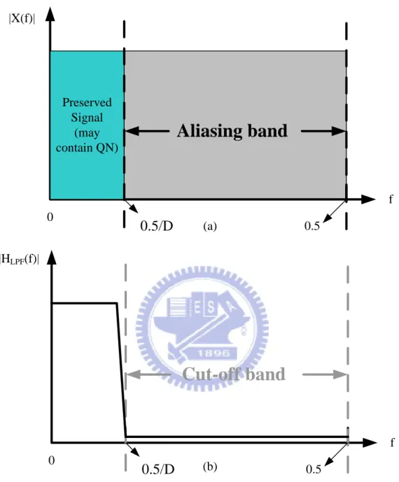
In this section, the terminologies related to design a decimator would be introduced, which include the parameters for designing low-pass filter and some considerations in down-sample procedure. For down-sampling D, the aliasing-band of signal and cut-off-band of low-pass filter designed to prevent aliasing is shown below.
~ 18 ~ f 0.5 Preserved Signal (may contain QN)
0.5/D
Aliasing band
0 f 0.50.5/D
Cut-off band
0 |X(f)| |HLPF(f)| (a) (b)Figure 1.15 (a) Aliasing-band of signal (b) cut-off-band of low-pass filter designed to prevent aliasing
From above Figure 1.15, it is clear that the signal in aliasing band is required to be removed due to the relationship between x[n] and xd[n] expressed by Equation 1.24
Chapter 1: Introduction ~ 19 ~
Downsampler
↓D
xd[n] x[n] Figure 1.16 Downsampler xd n = x[nD] (1.24)And the relationship between x[n] and xd[n] in frequency domain (discrete-time
Fourier transform) is
Xd f =D1 D−1i=0 X(Df −Di) (1.25)
X(f) and Xd(f) are discrete-time Fourier transform of x[n] and xd[n], respectively.
Now, from Equation 1.25, it could explain why the aliasing-band is in the range [0.5/D, 0.5] in Figure 1.15(a) because Xd(f) is D copies of X(f) with expanding D
times in frequency domain and shifted by integer multiples, which imply that 0.5/D in frequency domain would be expanded to 0.5 and thus larger than 0.5/D in frequency domain would overlap (expanded to >0.5) with other copies X(f/D-i/D). For example D=4, Xd(f) aliased by other copies of X(f/D-i/D) (i.e., i=1,2,3) is shown below.
0.5 -0.5 0 1 2 3 4 -1 -2 -3 -4 …… …… 0.5 -0.5 0 1 2 3 4 -1 -2 -3 -4 ~ ~ ~ ~ ~~ ~~
i=1 i=2 i=3 i=0 blue f f X(f) Xd(f) (a) (b) i=1 i=2 i=3
i=0 blue
i=0 blue
D=4
~ 20 ~
From above Figure 1.17, it is obvious that there are D-1 copies (D=4) aliased to the band [-0.5, 0.5]. In a word, frequency of signal larger than 0.5/D in [0, 0.5] would cause aliasing. Now, considering a case OSR>D (first few stages of multi-stages decimator), aliasing would still exist. However, only a few bands in aliasing band [0.5/D, 0.5] alias to the wanted signal due to OSR>D, shown in Figure 1.18. And these few bands in aliasing-band aliasing to wanted signal are called folding band. Aliasing-band exclude folding-bands would alias to the unwanted signal (such as, quantization noise), which could be removed latter by remaining filters.
0.5 -0.5 0 1 2 3 4 -1 -2 -3 -4 ~ ~ ~ ~ ~~ ~~
i=1 i=2 i=3 i=0
blue
f i=1 i=2 i=3
i=0 blue i=0 blue Xd(f) wanted signal (green) D*fb D=4
Figure 1.18 The bands in aliasing band [0.5/D, 0.5] alias to wanted signal (green band), called folding-band, D=4.
Xd(f) i=1 -0.5 0.5 0.5 -0.5 1 2 3 0 4 -1 -2 -3 -4 f i=2 i=2 i=3 fb fb fb 1 D=4 i=3 i=1 i=2 i=2 0.5 -0.5 fb 1/D+fb 1/D-fb -fb -1/D+fb -1/D-fb 0.5-fb -0.5+fb f f f D=4
Figure 1.19 The bands over [-0.5, 0.5] overlap with wanted signal band are folding-bands, which are found from the trace-back process in this demonstration.
Chapter 1: Introduction ~ 21 ~ 0.5 1 f fb 1-fb
……
1/D 2/D (D-1)/D 1/D+fb 1/D-fb (D-2)/D 2fb folding bands wanted signal Band (in-band) 2fb 2fb 2fb 0 Aliasing-band 0.5/D wanted signal Band (in-band)Figure 1.20 There are D-1 folding-bands for down-sampling D.
Signal (might be quantization noise) on folding-bands would alias to wanted signal (in-band signal), which could not separate and recover by remaining filter, so signal on folding-bands must be attenuated more. Folding-bands of signal are shown in Figure 1.20. Also, these bands are derived from Equation 1.25. Note that the frequency range in Figure 1.20 is [0, 1], which is convenient for calculating aliasing power by FFT in matlab and understanding from Equation 1.25. On the other hand, the frequency range [0, 1] makes the folding-band not split at frequency 0.5, which is the reason why the frequency range [-0.5, 0.5] is usually chosen to depict signal (make the signal-band continuity at frequency 0).
Now that the folding-bands are known, the parameters in filter design (filter specifications), especially for low-pass FIR filter, could be introduced.
~ 22 ~ Fs Fp Rs +Rp -Rp Passband Transition band Stopband Magnitude (dB) Rp 0.5 0 0 f Rp 0 dB
Figure 1.21 Filter specifications for low-pass filter
Rp: pass-band ripple (dB), maximum deviation in pass-band Rs: stop-band minimum attenuation (dB)
Fp: end frequency of pass-band Fs: beginning frequency of stop-band
These are parameters in designing low-pass filter, and the decisions of these parameters influence the aliasing power of folding-bands, which are discussed further in Chapter 2.
1.3 A Brief Introduction of Proposed Solution
As mentioned in motivation (Section1.1), the high order FIR filter, which comprises many multipliers, adders and registers, dominates large silicon area in decimator of the sigma-delta A/D converter. A technique, time-multiplexing (folding), could be used to reduce the number of functional units (such as multipliers and adders), so as to minimize the silicon area of integrated circuits. The basic idea of folding is to execute multiple algorithm operations on a single functional unit by time-multiplexing (to finish the same operations by more clock cycles using fewer functional units), so the number of functional units is reduced. For example, it could be time-multiplexed as one multiplication operation finished in each cycle using 100 times faster clock, which only demand one multiplier, if 100 multiplication operations are required to finish in one clock cycle. And the technique, folding, is very suitable
Chapter 1: Introduction
~ 23 ~
for decimator due to the much lower sampling-rate at the input of high order FIR filter, which imply that there are many clock cycles could be used by each sample and a faster clock is not needed.
In order to minimize the silicon area of high order FIR filter, the technique, folding, is used to obtain acceptable minimum multipliers and adders. Furthermore, the transposed-form structure has been adopted to reduce half registers, which could merge together in polyphase decomposition. Now, the basic idea to obtain minimum hardware is achieved. However, it is hard to use folding technique to transposed-form structure with acceptable power consumption. This thesis proposed a design methodology based on transposed-form folding, which change the computation procedure to preserve the half register benefit and maintain lower power consumption by using extra control circuits, for FIR filter with polyphase decomposition.
For the programmable decimation ratio requirement, IIR-FIR structure of comb filter is adopted in the first stage of decimator to ease the design of the different low-pass filter spectrums, which are different in pass-band edge. Moreover, the pass-band drop of designed filter spectrums by IIR-FIR comb filter could be compensated by the same compensation filter. These means that no extra filter hardware is needed to produce different low-pass filter spectrum to prevent aliasing.
This thesis focuses on comparison of different folding implementation in area, power, speed and etc. So, the specification of sigma-delta modulator is not a main issue wanted to discuss in this thesis. A case of 1-bit, OSR 128 and 64, 4th-order SDM is chosen as a specification of the sigma-delta A/D converter. And then the decimator would be designed to meet the requirements of that SDM specification. Usually, the designed decimator could be used for most SDM specifications, lower than 4th-order and OSR=128 or 64. As a result of that one bit SDM A/D converter don’t require D/A circuit, one bit SDM is often chosen to implement. These make designed decimator more useful.
1.4 Thesis Organization
In Chapter 2, architecture (number of stages and decimation ratio of each stage) and filters specification of decimator are decided to meet the requirements of determined sigma-delta modulator, 1-bit 4th-order, OSR=128,64 SDM.
~ 24 ~
in Chapter 3. Also the advantages of this thesis proposed implementation method for high order FIR filter are shown in Chapter 3. Finally, it has been verified that the proposed implementation methodology is suitable for any order, number of quantizer bit, and OSR SDM as well as its advantages would still exist.
In Chapter 4, testing environment and instrument are introduced. And function testing results and electrical characteristic of decimator, which is fabricated in TSMC 0.18um CMOS mixed signal RF general purpose MiM Al 1P6M process, would be plotted and summarized.
Chapter 2: Decimator Architecture and Design ~ 25 ~ __________________________________
CHAPTER
2
__________________________________Decimator Architecture and Design
In this chapter, decimator architecture (number of decimation stages and decimation ratio of each stage) and decimation filter specifications (order of each filter according to designed pass-band ripple, pass-band edge, stop-band attenuation, and stop-band edge; these definitions see Figure 1.21.) are decided so as to meet the SNR requirements of pre-defined sigma-delta modulator specifications (1-bit 4th-order, OSR=128, 64 SDM) with efficient decimator hardware in terms of functional units and power consumption.
2.1 Considerations about SDM Quantization Noise
These in-band quantization noise power of 1-bit 4th-order, OSR=128, 64 SDM are 9.5134 × 10⁻¹⁸ and 4.8711 × 10⁻¹⁵ (see section 1.2.2 and Equation 1.22, using V=1
for convenience), respectively. And sinusoidal signal power with maximum amplitude, namely V=1, is 0.5. As a result of that, the ideal peak SNR are 10log(0.5/9.5134 × 10−18)=167.2 dB and 10log(0.5/ 4.8711 × 10⁻¹⁵)=140.1 dB for OSR=128 and
OSR=64, respectively. However, the quantization noise power at SDM output (before decimator) is (similar to Equation 1.22):
QN = 0.5 Pe f He f 2 df −0.5 =( 2 2N)2 12 2 2k 0.5 sin2k πf df −0.5 (2.1)
~ 26 ~
N: number of quantizer-bit k: order of SDM
sinnu du = −sinn −1u cos u
n +
n−1
n sinn−2u du (2.2)
The result of Equation 2.1 could be obtained by using integral formula of Equation 2.2 [4].
Furthermore, numerical methods could be used to solve the Equation 2.1 in Matlab for known N and k. In this case (N=1 and k=4), quantization noise power of SDM output calculated in Matlab is 5.83, which is much larger than in-band quantization noise power (9.5134 × 10⁻¹⁸ with OSR=128 and 4.8711 × 10⁻¹⁵ with
OSR=64).
As a result of that, the decimator design procedure must take care of quantity of quantization noise power, especially in folding-bands (alias to in-band in decimation procedure). The target aliasing power in my decimator design procedure is ten times as small as in-band quantization noise power, so the SNR would not degrade more than 0.41 dB (10 log 1.1∗QNsignal power
in −band = SNR − 0.41 dB) after decimator.
Before proceeding, some concepts of spectrum in discrete-time signal or digital filter must be reminded. For example, shaped quantization noise power spectral density could be shown as Figure 2.1(a) or Figure 2.1(b) or Figure 2.1(c):
0 0.1 0.2 0.3 0.4 0.5 0 5 10 15 20 25 frequency PSD Quantization Noise of SDM 0 0.2 0.4 0.6 0.8 1 0 5 10 15 20 25 frequency PSD Quantization Noise of SDM -0.50 0 0.5 5 10 15 20 25 frequency PSD Quantization Noise of SDM
=
=
(a) (b) (c)Figure 2.1 (a) frequency over [-0.5, 0.5] (b) frequency over [0, 1] (c) frequency over [0,0.5]. The signals represented by these figure are the same.
Although the graphs of Figure 2.1 are quite different, the signals shown by these figure are the same, which could be recognized over the range [0, 0.5]. Because
Chapter 2: Decimator Architecture and Design
~ 27 ~
spectrum of discrete-time signal is periodically repeated, only one period should be depicted, which means that the ranges over [-0.5, 0.5] or [0, 1] could be chosen to depicted. For real number signal, its spectrum is even function, which means X(-f)=X(f), and then only half periodic spectrum is needed to depict, i.e. the range over [0, 0.5].
In the following design procedure, signal or filter spectrum would be depicted over the range [0, 1] (like Figure 2.1 (b)), which match the FFT points [0, N-1] in Matlab and is easy to illustrate folding-bands of signal.
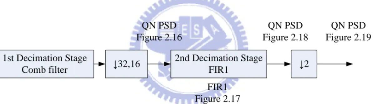
2.2 Decimator Architecture
Decimation is often performed in several stages [5], which reduces the number of algorithmic operations per second and the required functional units in decimator, especially for high OSR (OSR>4). First of all, the components of multi-stages decimator must be decided as well as the number of decimation stages. The most efficient choice for first decimation stage is comb filter (also called sinc filter), which don’t require multiplier and attenuates aliasing-band signal enough (especially attenuate more for folding-bands signal) [6]. According to analysis in [7], the appropriate decimation ratio of comb filter is OSR/4 for sigma-delta modulation (32 and 16 for OSR=128 and 64, respectively), which results in most efficient algorithmic bit-operations per second considering word-length of comb filter and the required sampling rate at each components of comb filter.
Furthermore, the remaining four times Nyquist rate would be decimated by FIR filters, which could approximate to an ideal low-pass filter that would perfectly preserve in-band signal and exactly remove out-of-band quantization noise due to its sharp roll-off if the order of FIR filter is high enough. According to analysis in [5], two stages FIR filters structure with each decimation ratio 2 is an efficient implementation for decimating four times Nyquist rate signal.
Three stages decimator architecture is an efficient implementation, which is good enough for attenuating aliasing power to obtain required SNR. However, the pass-band drop due to comb filter is slightly severe, which make the in-band signal perfectly preserved by FIR filters worse, especially order and decimation ratio of comb filter are high. For example, 5th-order comb filter with decimation ratio 32 would cause the pass-band drop of OSR-128 signal more than 1 dB, which destroys the effort made by FIR filter in terms of suppressing pass-band ripple. Usually, the compensation filter is introduced and combined with low-pass filter, which means that a single FIR filter in
~ 28 ~
the 3rd-stage of decimator is used to remove quantization noise, prevent aliasing and compensate the pass-band drop due to comb filter. The hardware complexity is not increased; however, the features of compensation filter and low-pass filter slightly conflict with each other over the frequency [0.23, 0.25] because one (the compensation filter) need to go up in magnitude to compensate pass-band drop and the other (the low-pass filter) need to go down to prevent aliasing. As a result of that, the quantization noise over [0.25, 0.27] didn’t be removed very well and the pass-band drop also didn’t be compensated very well over entire in-band (worse near 0.23 in frequency).
In this work, the compensation filter and the low-pass filter are separated to provide a better solution in terms of suppressing pass-band ripple and attenuating aliasing power.
5th Comb Filter ↓32,16 FIR1 ↓2 FIR2 ↓2 FIR3
Compensation
5th Comb Filter ↓32,16 FIR1 ↓2 FIR2 ↓2
5th Comb Filter ↓32,16 FIR ↓4
Decimation Filter ↓128,64 [6] [5] (1) (2) (3) (4)
Comb filter is the most efficient choice for first decimation stage
Two stages FIR filters structure with each decimation ratio 2 is an efficient implementation
Better for suppressing aliasing power and compensating pass-band drop
Figure 2.2 Decimator architectures
A numerical demonstration of the different decimator architectures for 1-bit 4th-order OSR-128 is shown below:
Chapter 2: Decimator Architecture and Design
~ 29 ~
5th Comb Filter ↓32 FIR1 ↓2 FIR2 ↓2 FIR3
Compensation
5th Comb Filter ↓32 FIR1 ↓2 FIR2 ↓2
5th Comb Filter ↓32 FIR ↓4
Decimation Filter ↓128
(1)
(2)
(3)
(4)
For 1b 4th-order SDM OSR=128
Order of FIR=10495
Obtained SNR=164.47 dB P=fs/128*10496/128*128=82fs
P=Number of required multiplication operations per second
Order of FIR=260
Obtained SNR=165.9 dB P=fs/32/4*261/4*4=2fs
Obtained SNR=166.4 dB
Order of FIR1=18 Order of FIR2=126
Rp=0.01 dB P=fs/32/2*19/2*2+fs/64/2*127/2*2=1.29fs
Obtained SNR=167.2 dB Rp=0.002 dB Order of FIR1=18 Order of FIR2=126 Order of FIR3=40
P=fs/32/2*19/2*2+fs/64/2*127/2*2+fs/128*41=1.6fs
Obtained SNR=166.7 dB Rp=0.009 dB P=fs/32/2*19/2*2+fs/64/2*201/2*2=1.87fs Order of FIR1=18 Order of FIR2=200
Figure 2.3 For 1-bit 4th-order OSR-128 SDM, decimator architectures in terms of SNR, number of required multiplication operations per second and pass-band ripple
are shown.
2.3 First Decimation Stage
As mentioned in previous section, the features of comb filter, which don’t require multiplier, suppress folding-bands signal excellently, attenuate out-of-band signal well and could have large decimation ratio to lower the sampling rate for later FIR filter, are suitable for the first decimation stage operating in the fast sampling rate. The transfer function of comb filter (also called sinc filter) is:
Hcomb z = D1k(1−z1−z−D−1)k (2.3) = D1k (1 + z−2i )k (log2D)−1 i=0 (2.4) = D1k( D−1z−i) i=0 k (2.5)
~ 30 ~
k: order of comb filter D: decimation ratio
For k=5 and D=32, its zero-pole plot and frequency response are show below:
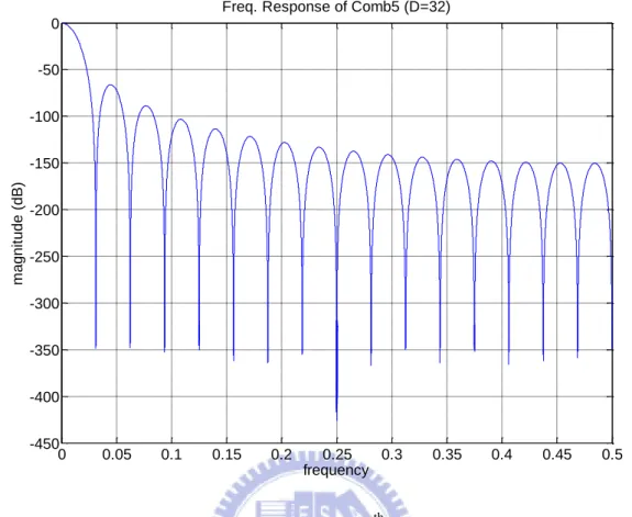
Figure 2.4 zero-pole plot for 5th-order comb filter with D=32
(5*32 zeros around unit circle, 5 poles in z=1 and the other poles in z=0)
-1 -0.5 0 0.5 1 -1 -0.8 -0.6 -0.4 -0.2 0 0.2 0.4 0.6 0.8 1 5 5 5 5 5 5 5 5 5 5 5 5 5 5 5 5 5 5 5 5 5 5 5 5 5 5 5 5 5 5 5 5 155 Real Part Im a g in a ry P a rt
Chapter 2: Decimator Architecture and Design
~ 31 ~
Figure 2.5 Magnitude frequency response of 5th-order comb filter with D=32 (half periodic spectrum have been depicted, so there are D/2=16 notches in spectrum)
Recent researches on first decimation stage filter are also based on comb filters, which would be introduced in following section.
2.3.1 Introduction to Modified Comb Filters
Novel decimation schemes based on comb filter are proposed by [8]-[10]. The basic idea is to rotate the zeros of comb filter to obtain a better rejection around folding-bands. As seen in Figure 2.4, there are 5 zeros in the same position for 5th-order comb filter. If the zeros could be distributed around folding-bands (not all zeros in the same position (middle of folding-band)), a better rejection around folding-bands can be achieved.
The transfer function of counterclockwise rotated 1st-order comb filter could be defined as [9]: Hq+ z =1 D 1−z−DejαD 1−z−1ejα (2.6) 0 0.05 0.1 0.15 0.2 0.25 0.3 0.35 0.4 0.45 0.5 -450 -400 -350 -300 -250 -200 -150 -100 -50 0
Freq. Response of Comb5 (D=32)
frequency m agn it ude (dB)
~ 32 ~
And the transfer function of clockwise rotated 1st-order comb filter could be defined as:
Hq− z =1
D
1−z−De−jαD
1−z−1e−jα (2.7)
In order to obtain real number coefficient, the Equation 2.6 and Equation 2.7 must be combine together to form the transfer function:
Hq z = Hq+ z Hq− z = 1
D2
1−2cos (αD)z−D+z−2D
1−2cos (α)z−1+z−2 (2.8)
The transfer function of modified comb filter consists of Hcomb(z) and Hq(z).
The kth-order modified comb filters (MCF) mean that there are k zeros distributed around the folding-band. And the transfer functions of different order MCF are defined as follow:
HMCF 3 z = Hcomb 1 z Hq(z) (2.9)
HMCF 4 z = Hcomb 2 z Hq(z) (2.10)
HMCF 5 z = Hcomb 1 z Hq1(z)Hq2(z) (2.11)
HMCF 6 z = Hcomb 2 z Hq1(z)Hq2(z) (2.12)
MCF3, MCF4, MCF5 and MCF6 denote 3rd-order, 4th-order, 5th-order and 6th-order modified comb filters, respectively. Also, Hcomb1(z) and Hcomb2(z) denote the
transfer function of 1st-order and 2nd-order comb filter, respectively.
Chapter 2: Decimator Architecture and Design ~ 33 ~ α α α α α α D=4
=>
D=4 k=3+
+
(a) Hcomb1 (b) Hq+ (c) H q-(d) HMCF3 In-band folding-bande
j2πfbe
-j2πfbFigure 2.6 zero-pole plot of (a) 1st-order comb filter (b) counterclockwise rotated of 1st-order comb filter (c) clockwise rotated of 1st-order comb filter (d) 3rd-order
~ 34 ~ 0 0.1 0.2 0.3 0.4 0.5 0.6 0.7 0.8 0.9 1 -200 -180 -160 -140 -120 -100 -80 -60 -40 -20 0 frequency M a g n it u d e R e s p o n s e MCF3 with D=4
folding-band folding-band folding-band
Figure 2.7 Magnitude response (dB) of 3rd-order modified comb filter (MCF3) with D=4
The optimized rotated angle α to obtain maximum rejection around folding-band has been presented by [9]. Now, fb denotes the in-band edge. The optimized rotated
angle α can be rewrite as follow:
α=q2πfb (2.13)
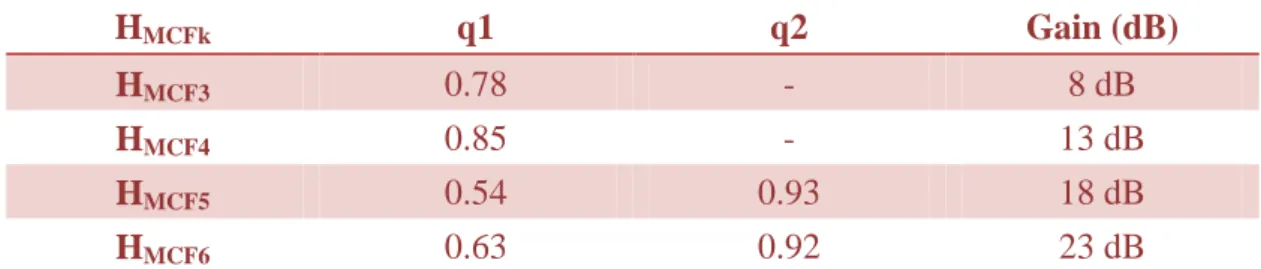
then optimized q for different orders MCF are [9]:
Table 2.1 Optimized rotated angle α represented by q, which is independent to fb.
HMCFk q1 q2 Gain (dB)
HMCF3 0.78 - 8 dB
HMCF4 0.85 - 13 dB
HMCF5 0.54 0.93 18 dB
Chapter 2: Decimator Architecture and Design
~ 35 ~
Gain = quantization noise of SDM in folding bands after comb filter quantization noise of SDM in folding bands after MCF
= |Hcomb −k(f)|2PeSDM f df i D+fb i D−fb D−1 i=1 |HMCF −k(f)|2PeSDM f df i D+fb i D−fb D−1 i=1 (2.14) 0.23 0.235 0.24 0.245 0.25 0.255 0.26 0.265 0.27 -300 -250 -200 -150 -100 -50 0
Comb3 and MCF3 with D=4
frequency M agn tude R es pon s e (dB) Comb3 MCF3
Figure 2.8 Magnitude responses of Comb3 and MCF3 in folding-band. The MCF3 can suppress more quantization noise power in folding-band.
2.3.2 Stage1 Design
As mentioned in the introduction of Chapter 2, aliasing power is the main concern in the design procedure of decimation filter. The quantization noise are 9.5134 × 10⁻¹⁸ and 4.8711 × 10⁻¹⁵ for 1-bit 4th
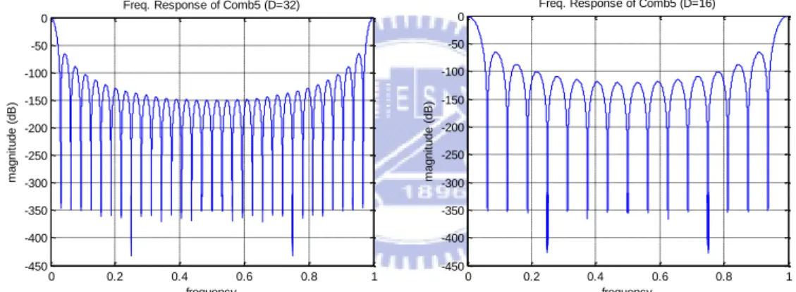
-order, OSR=128, 64 SDM, respectively. The aliasing power of first decimation filters must be smaller than the ideal in-band quantization noise power of SDM. And four times Nyquist rate would be left for later FIR filters to decimate [7], i.e. D=OSR/4.
![Figure 2.1 (a) frequency over [-0.5, 0.5] (b) frequency over [0, 1] (c) frequency over [0,0.5]](https://thumb-ap.123doks.com/thumbv2/9libinfo/8345058.176184/41.892.141.746.820.987/figure-frequency-b-frequency-c-frequency.webp)