A 2.4 GHz CMOS Image-Reject Low Noise Amplifier
Ming-Chang
Sun.
Shing Tenqchen
*,
Ying-Haw Shu. Wu-Shiung Feng
Lab 331, Department of Electrical Engineering,
National Taiwan University, Taipei, Taiwan, R.
0.
C.
*NTU-EE Also with Chunghwa Telecom Telecommunication Labs., 12, Lane 5 5 I, Sec. 5, Min-Tsu Rd., Yang-Mei Zien, Tao-Yuan County, Taiwan 326, R.O.C.
E-mail: [email protected]
Abstract
In this paper, a new image-reject low noise amplifier is
designed for the 2.4 GHz industrial-scientific-medical (ISM)
band. An inter-stage T-structure filter is used in the low noise amplifier design to provide 35-dB image rejection. The goal of this design is to merge the image-reject function into the low noise amplifier.
l.,
Introduction
Low noise amplifier. is a fundamental building block in radio frequency front-end circuits. Its function is to amplify very small radio frequency signal while suppressing the noise of the circuit itself. Two major receiver architectures, heterodyne and homodyne, are widely adopted in transceiver designs. Each of the architectures has its own advantages and drawbacks. Homodyne architecture receiver, for instance, has higher level of integration due to its image-free architecture, but the DC offsets issues are hard to deal with. By contrast, heterodyne architecture receiver needs an image-reject filter to remove the unwanted image frequency signal. Due to the high frequency of GHz range, the image-reject filter is often an expensive off-chip surface acoustic wave (SAW) filter. In this paper, a T-structure filter
is used to design with a low noise amplifier at 2.4 GHz
intended for the up coming IEEE 802.1 lg standard.
The cascode structure as shown in Fig. 1 is known as the
best architecture that can achieve both power gain and low noise figure (NF) requirements. The input impedance is usually matched to 50 ohms due to the sensitivity of the front-end duplexer filter to the input impedance of the low noise amplifier.
Figure 1. Cascode low noise amplifiei
The matching condition of the input impedance is often difficult to achieve due to the process variation and the lack of good active and passive device models. The input impedance ofthe cascode LNA is given by [I]
where
g,,
andcgs,
are the transconductance and gate-source capacitance of the MI transistor, respectively. Because of the required 50 ohms input matching the source inductor is usually very small. Therefore, a large gate inductor is required to tune out the gate-source capacitance of the MItransistor.
The common-gate transistor M2 acts as a current buffer that provides impedance transformation and higher isolation between output and input of the low noise amplifier. In order to reduce the gain loss at the inter-stage node of the two transistors, an inter-stage matching scheme using inductor was studied [2]. The drawback is the somewhat greater Miller effect of gate-drain capacitance of the MI transistor. Although the inter-stage matching scheme using only one inductor achieves the inter-stage impedance matching, it still requires perhaps an expensive off-chip SAW filter if it were used in the heterodyne receiver architecture. In this paper, a 4th-order T-structure filter is designed to provide additional image-reject ability while achieving inter-stage impedance matching.
2.
Proposed Image-Reject
LNA
Shown in Fig. 2 is a 4th-order T-structure filter, where
2,
is the impedance, including the parasitic capacitance, seen into the source of the M2 transistor. Since the M2 transistor of the low noise amplifier in Fig. I acts as a current buffer, the transfer function of the output current tothe input current of the T-structure filter is of interest.
4Trz-j7&
.- - .
Figure 2. T-structure filter The current transfer function is given by
where the zero frequency is
(3) This zero frequency is designed at the image frequency when the T-structure filter is integrated into the cascode low- noise amplifier.
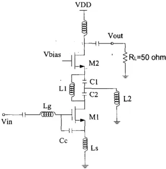
A proposed low-noise amplifier using the T-structure filter is shown in Fig. 3 where the bias circuitry is not detailed.
The purpose of the T-structure filter is to suppress the image frequency signal while providing inter-stage matching. The image frequency is the zero frequency of the T-structure filter as described above. Due to the complex current transfer function, the inter-stage impedance matching is achieved by circuit simulation.
V D D Vbias_( R ~ = 5 0 ohm M2
L2
MI Vin cc Ls&
Figure 3. Proposed low noise amplifier
The capacitance Cc placed between gate and source of the M I transistor is used to help easier input impedance matching [2]. The required on-chip gate inductor is reduced, thus the area of on-chip gate inductor is significantly reduced. The result is that the signal loss in the input path is
decreased and the reduced power gain due to the Cc
capacitor is compensated.
The image-reject low noise amplifier proposed is designed to operate at 1.5 V power supply. The T-structure filter does not consume any power. The complete circuit is simulated using TSMC 0.25
jlm
CMOS technology. The circuit chip implementation is shown in Fig.I.
Some of the design parameters are summarized in Table 1 .Operating frequency
Table I . Some of the design parameters
2.4 GHz
Power supply 1.5 V
Inductance of L I , L2 Capacitance ofC1, C2 WILofM1,MZ
requirements. This is because the device models used in the circuit simulations are not ideal. The circuit can be further optimized to boost up the power gain. A second buffer stage
can also he used to achieve higher power gain at the cost of more power consumption.
4.3nH 2 PF 500 Sll. S21 parameters g . 2 0 . . . ... 1 0 1.5 2.0 2.5 3.0 3.5 freq, GHr
3. Simulation
Results
The proposed low noise amplifier is simulated with Agilent Advanced Design System. The TSMC 0.25
p
CMOS device models are used in this simulation. The foundry provided CMOS device models are calibrated, that is, the non-ideal properties of the CMOS process is incorporated into the device models. The target operating frequency is the 2.4 GHz ISM band. The image frequency is chosen at 1.8 GHz with the local oscillator frequency at 2.1
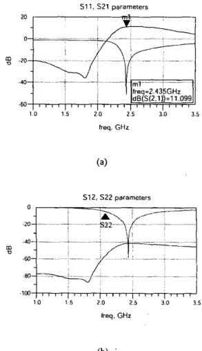
GHz. Thus, the resultant intermediate frequency (IF) is located at 300 MHz. The higher IF frequency is because it is difficult to put the image frequency closer to the peak point of the power gain. Shown in Fig. 4 are the simulated S
parameters. In Fig. 4(a), the curve with the mark m l is the simulated S21, which is the power gain. It can be seen that the image-reject low noise amplifier suppresses the image frequency signal up to 35-dB. However, the power gain of the low noise amplifier i s somewhat lower than the general
S12, S22 parameters ... ... m D 1 .a 1 5 2.0 2.5 3.0 3.5 Ireq. GHr (h)
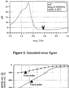
Figure 4. Simulated (a) SI 1, S21, (b) S12, S22 parameters Fig. 5 shows the simulated noise figure. .The signal at the image frequency is suppressed, thus, the noise figure at that frequency is very large. The noise figure is about 3 dB, and it can be decreased further by boost up the power gain of the M 1 transistor of the low noise amplifier. Another issue that is important in the design of low noise amplifier is the nonlinear behavior. Third order intercept point is commonly
used as a measure of the degree of nonlinearity. Shown in Fig. 6 is the IP3 simulation; the IIP3 is about -10 dBm.
Noise Figure freq=2 435GHr “f(21=2 957 20 , . . . 10 3 5 3 0 2 5 2 0 I 5 1 0
Figure 5. Simulated noise figure
..., .
. .... . ... . .. . . . .. . .. . .. . .
Figure 6. Third order intercept point simulation
4.
Conclusions
An image-reject low noise amplifier using a 4th-order T-structure filter is proposed. The designed image-reject low noise amplifier operates at 1.5 V power supply and provides 35-dB image-reject ability while consuming no additional power. The complete low noise amplifier circuit is simulated and implemented using TSMC 0.25
pm
CMOS technology. The foundry provided device models are calibrated to incorporate the non-ideal properties of the CMOS process.References
Derek K. Shaeffer, and Thomas H. Lee, “A IS-V,
1.5-GHz CMOS Low Noise Amplifier,” IEEE J.
Solid-state Circuits, vol. 32, pp. 745-759, May 1997.
Giovanni Girlando, and Giuseppe Palmisano, “Noise Figure and Impedance Matching in RF Cascode Amplifiers,” IEEE Trans. Circuits and Systems, vol. 46,
pp. 1388-1396, Nov. 1999.
Hong-Sun Kim, Xiaopeng Li, and Mohammed Ismail, “A 2.4 GHz CMOS Low Noise Amplifier using an Inter-stage Matching Inductor,” Circuit and System,
2000. 42nd Midwest Symposium, vol. 2, pp. 1040-1043,
2000.
Thomas H. Lee, H i n d Samavati, and Hamid R. Rategh “S-GHz CMOS Wireless LANs,” IEEE Trans. Microwave Theory Tech., vol. 50, pp. 268-280, Jan.
2002.
Jie Long, Nader Badr, and Robert Weber, “A 2.4Ghz Sub-ldB CMOS Low Noise Amplifier with On-Chip lnterstage Inductor and Parallel Intrinsic Capacitor,” IEEE Radio and Wireless Conference, 2002. RAWCON
2002. pp.165 -168,2002
Figure 7. Chip layout