Design and Implementation of a Highly Efficient VLSI Architecture
for Discrete Wavelet Transform’
Chu Yu, Chien-An Hsieh,
a n dSuo-Jie Chen
Qepartment
of
Electrical Engineering National Taiwan University,Taipei. Taiwan,
R.O.C.
Abstract
Since the discrete wavelet transform (DWT) is a kind of multi-rate transform, it is difficult to design an optimal computation-time architecture for the DWT. In this paper, we propose a highly efficient VLSI architecture for the 1-D DWT decomposition. This architecture contains two stages
of systolic decimation filter banks to guarantee a high throughput and an optimal computation time. Using this architecture, N-point samples with J resolution levels can be computed in N clock cycles spending only JL registers, where L denotes filter length. Due to its regular structure, this architeawe can be easily scaled up with the tap size of the. filters and the number of octaves. The performance of the proposed architecture will be verified by the successful implementation of a 4-tap 3-octave DWT VLSI chip.
1. Introduction
The discrete wavelet transform provides a new method for signal processing 111-[2]. It decomposes data into components of different frequencies, such that we can have good time resolution at high frequencies and good frequency resolution at low frequencies. The wavelet transforms are well suited for analyzing physical situation where signal contains discontinuities and sharp spikes. Recent developments have led the DWT into many applications such as audio and image compression, image recognition system, transient signal analysis, computer graphics, and so
on.
For real-time and high-speed applications, a dedicated DWT hardware device is needed and several VLSI
architectures have been proposed [3-61. Knowles [3] proposed the first VLSI architecture for the I - D B W T . Later, Parhi and Nishitani [4] proposed a folded and a
digit-serial architectures for the I-D DWT. T h e Patter two architectures have fixed-size D W T octave, and are not designed t o scale up with the number of octaves and the size o f the filters. Therefore, Fridman and Manolakos[5] proposed a multiprojection based systolic architecture for t h e 1-D DWT. In addition,
Vishwanath et al. [ 6 ] proposed three routing-network based systolic architectures for the I-D DWT. These
f
This work was supported by National Science Council, unde grants NSC 86-221 5-E002-034 and NSC 86-2221-E002-066
11.
1 -D DWT architectures [5]-[6] are scalable. but their input sequence has to interleave. thus deriving lower throughput.
In this paper, w e present a scalable VLSI architecture which can compute data on-the-fly, i.e., the input data can be processed at the rate o f one sample per clock cycle. In our design, all the computations of DWT. except those of the first octave, are folded into the computations o f the second octave. Thus, this folded architecture can provide an ideal high throughput and still retain its scalability. I n addition, a 4-tap 3-octave DWT chip has been implemented to verify the performance o f the proposed architecture.
2.
Discrete Wavelet Transform
The wavelet transform (WT) is a kind of time-scate decomposition of signals. The WT and Short-time Fourier transform (STFT) differ in their time-frequency representations. The WT processes data with different window widths at different scales (frequencies), which overcomes the limitation of fixed time-frequency resolution of STFT.
The discrete wavelet transform of a signal x ( t ) is given by:
W ( h . o ) = - Y
&”’
( ) ’ h(‘3
-where b is the time factor, a is the scale factor, h(t) is the wavelet basis function. Properties of wavelet transforms are heavily dependent on their basis wavelet functions.
,
fl:*
fl4Fig. 1 A 3-octave filter bank tree for the I-D DWT The DWT can also be viewed as a kind of multiresolution decomposition of a sequence. By exploring the subband
scheme recursively, a fast DWT can be constructed. Figure 1
shows a three-octave filter bank tree for the I-D DWT, where H(z) and G(z) represent a low-pass and a high-pass filters, respectively; and k2 represents subsampled by 2, by
4.1
dropping one every two samples. Assume an input sequence
~ ( n ) contains N samples, then the output sequence length should also be
N.
The first octave computes NI2 samples, the second octave computes NI4 samples, ..., and so on.M U X
3. VLSI Architecture for DWT
MUX
As mentioned above, a scalable architecture is our design goal. Therefore: in this section we present a novel and efficient VLSI architecture for the 1-D DWT decomposition, which performance is comparable with other previously proposed scalable architectures [ 5 ] - [ 6 ] . The overall
architecture is given in the following subsection and the decimation filter scheme is described in Subsection 3.2.
3.1 Overall Architecture
As shown in Fig. 1 , we need to compute N-point samples in the first octave, then generate NI2 output samples. Similarly, in the second octave, we need to compute NI2 input samples and generate NI4 output samples. For an nz-
octave DW-T. tile total number of samples to compute is:
Ri + (+>& + (+)‘A’+...+(+)”’-’ N = 2N(1 - 2 - ” ’ ) < 2N ( 2 ) Assume one filter bank can compute N samples in one unit time. at most two filter banks.are needed to generate all the discrete wavelet transform coefficients. Therefore, our proposed architecture looks like a folded architecture as shown in Fig 2.
.&.
o.,.vr I
Fig. 2 Overall architecture
The input sequence of the second octave is periodic ( N l 2 ) and generates an output every two clock cycles (Nl4), and the output at the third octave is thus one sample every four clock cycles ( N / 8 ) , and so on. The computations of all the octaves after the second octave can be folded into the second-octave filter bank. by cleverly inserting the remaining octave computations into the spacing in the sccond octave.
Generally, the folded technique is a very good approach to reducing hardware cost for iterative multistage computation, but it may cause a lower I 1 0 rate. Different with the other architectures, where all the computations are folded into a one-octave filter bank, we only folded the octaves after the second. In those methods, they have to interleave the computations of the first octave with those of the other octaves, such that their throughput may not achieve as high enough performance as we did.
MUX I MUX I
I I
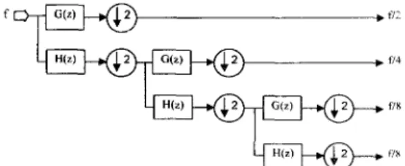
Fig. 3 Systolic decimation filter
Because not every output of the filter banks in Fig. 1 is needed, only one of every two outputs is generated. In Fig. 3. the filter does not generate every output but just the ones that are needed. An operation snapshot of Fig. 3 is shown in Table 1, where the transfer function of the filters is given by: (3 )
G(z)=g,,+ g,*z-‘ + g2*z-’+ g,*z-3
Table 1 : Operation snapshot of Fig. 3
In the above filter, only one control signal is used, and the number of multipliers and adders (MACs) is saved by a half compared
to
the conventional systolic filter, and the register number is saved by a half, too. Therefore, for an L-tap filter. the total number of MACs used in our architecture is 2*(L12)*2 = 2 L , which is the same as those architectures proposed in [ 3 ] - [ 6 ] . The register number is (L/2)*2*J = LJfor a J-octave DWT, which is much less than the others. Since the computations in octaves after the second octave are folded into the spacing of the second octave, the second- stage architecture is obviously different from the first stage. Figure 4 shows the second-stage architecture. The operations of the second stage are similar with the first stage. By n
correctly inserting the remaining octave computations into the second-octave spacing, all the computations of the DWT can be accomplished. As seen, the sequence
of
each octave i s generated periodically,so
the controller isa
simple binary counter. Moreover, each groupof
octave registers in Fig. 4 is controlled by a selection signal. For scaling up with the filter size, only a simple duplication of submodules is needed to extend the filter for longer-taps.Gate Count
i'
923 1 octave 2 octave 31
2974 x 2868 urn2 Core SizeDie Size
]
3804\3468umZ Fig. 4 The'second-stage architectureI
I
4.
Chip Design and Implementation
Package
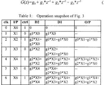
'To verify the performance of the proposed architecture, we have designed and laid out a DWT chip, which number of octaves is three and which filter size is four. In this section, we present the block diagram of the whole chip and the MAC cell. The input, output. and coefficient data are all
2's complement and %bit wide.
40 pin DIP
I
I I
Fig. 5 Block diagram of the chip
Figure 5 shows the block diagram of the whole chip. which consists mainly of two high-pass filters, two low-pass filters, and one controller. The operation of the whole chip has been described in the previous sections. Since the computations of all octave coefficients are interleaved, only one output port Is needed, which will save a number of pin count for the chip implementation.
4.1 Multiplication and Accumulation Cell
The multiplication and accumulation (MAC) cells are the major components in our design and occupy the most area of the chip. Fig. 6 shows the MAC cell block diagram used in our chip. We combine the multiplier and' the adder into one cell. The addition now becomes a partial product of the
multiplier. Then the delay time of a multiplier plus an adder.
is shortened to that of a multiplier. To further improve the speed, we adopt the modified Booth multiplier [8]-[9] to reduce half of the partial products For regularit) consideration, the partial products are simply added by using carry-save adders. The "final adders" were constructed with a 16-bit carry-select adder. having a 4-bit multiplexor based conditional-sum adder as its basic block.
1
c
I
X4
Booth Decode + Half Addersr
I
4
Booth Decode + Full Adders 1 It
r
16-bit Final AdderFig. 6 Block diagram of the MAC cell After the functional simulation performed using gate-level HDL in a Verilog-XL environment. this chip was synthesized using CADENCE tools and CCLO8-V 1 .O cell library from the Computer & Communication Research Laboratories, Hsin-Chu, Taiwan. This chip layout view is
shown in Fig. 7. Then, the VLSI chip was fabricated in a
O.8pm Single-Poly-Double-Metal CMOS technolog? through the Chip Implementation Center. National Science Council, R.8.C. And this chip has been measured with a
precise testing machine, IMS Logic Master ATS-200. to verify the intended perfomlance of the proposed I-D DWT architecture. A snapshot of the testing results was given in
Fig. 8. showing that the acquired values are q u a i to the expected values and that this chip works correctly The performance data is summarized in Table 2.
Table 2: Performance data
II
PowerI
855 mWI/
5.
Comparison
The comparison between our architecture with othei 5 1 5 shown i n Table 3. We choose only DWT architectuies with
scalablility to fair11 compare each other'< performance
Following [SI, we define some items fot the DW
r
performance. The design cost is the product of the bilicon
area used by registers and the delay of processing
M
input samples using a J resolution-level discrete wavelet tran5form.11.4.3
and L is the filter length. The improved ratio is generated by dividing the design cost of other architectures with ours. The comparison between our architecture with others is shown in Table 3 , where Vishwanath’s architectures include two approaches, one systolic and one semi-systolic architectures, respectively [6]. In the table, we see obviously each other’s performance according to their design cost and improved ratio.
Table 3: Comparison of various architectures
ratio
4JLM, 2JLM
Ours JLM
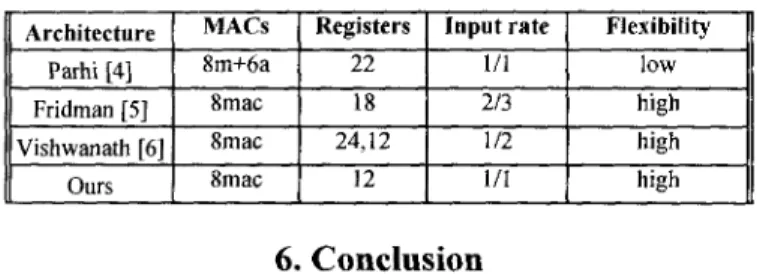
The comparison of the component numbers of our chip with others is shown in Table
4.
All are 4-tap 3-octave 1-Ddiscrete wavelet transform. Comparing with the non-scalable architectures [4], ours uses fewer registers. Comparing with the scalable architectures [5]-[6], ours has higher Performance and uses similar hardware components.
Table 4: Component counts of various architectures
11
ArchitectureI
MACS1
RegistersI
Input rateI
Flexibility1
high
1 12 high
Ours 8mac 111 high
6. Conclusion
A new high-efficient VLSI architecture for the 1-D DWT decomposition has been described in this paper. Compared to the general folded architecture which folds all t h e computatiorls into one filter bank, our folded two- filter-bank architecture can achieve high throughput, one sample per clock cycle, for the multi-rate transforms such as discrete wavelet transform. This architecture can also be easily scaled up with the size of the filters and the number of octaves by just using JL registers for a DWT with J octaves and L filter length. The successful implementation of a single chip verifies the intended and anticipated performance of our proposed architecture.
References
[ l ] I . Daubechies, Ten Lectures on Wavelets, vol. 61 of CBMS-NSF Regional Conferences Series in Applied Mathematics, SIAM, Philadelphia, PA, 1992.
(21 M. Vetterli, “Wavelet and filter banks: theory and design,” IEEE Trans. on Signal Processing, vol. 40, no. 9, pp.2207-2232, Sep. 1992.
[3] G. Knowles, “VLSI architecture for the discrete wavelet transform,’’ Electronics Letters, vol. 26, no. 15,
[4] K. Parhi and T. Nishitani, “VLSI architecture for
discrete wavelet transform, ” IEEE Trans. on VLSI
Systems, vol. 1 , no. 2, pp. 191-202, June 1993. pp.1184-1185, July 1990.
[5] 9. Fridman and E. S. Manolakos, “On the synthesis ot‘ regular VLSI architecture for the I-D discrete wavelet transform,” Proc. of S P l E Con$ on Mathematrcul Imaging: Wavelet Applications in Signal and lmuge
Processing 11, San Diego CA, J u l y 1994, pp.296-307. 51 M. Vishwanath, R. Owens. and M. J . Irwin, “VLSI
architecture for the discrete wavelet transform.“ IEEE Trans. on Circuits and Systems 11, analog and digital signal processing, vol. 42, no. 5 , pp.305-316. May 1995.
71 T. Miyazaki, T. Nishitani, M. Ishikawa, M . Edahiro. and K. Mitsuhashi, “Chrominance/Luminance signal separation and syntheses chips developed with a DSP silicon compiler,” PEEE Trans. on Circuits and Systems f o r Video Technology, vol. 2, no. 2, pp. 245-254. June
1992.
181 P. E. Madrid, B. Millar, and E. E. Swartzlander. J r . . “Modified booth algorithm for high radix fixed Point multiplication,” IEEE Trans. on VLSI Systems, vol. 1 . no. 2, pp.164-167, June 1993.
191 J. Fadavi-Ardekani, “MxN booth encoded multiplier generator using optimized wallace trees.” IEEE Truns on VLSISystems, vol. 1, no. 2, pp.120-125. June 1993.
Fig.7 Chip layout view
Fig. 8 Snapshot of testing on IMS ATS-200