nanotubes compared with the TiO2 nanotubes. On the contrary, under 0 V bias, quantum efficiency of the TiO2/AAO nanotubes
is 5.8 times lower than the TiO2nanotubes because of higher probability for the recombination of photon-generated electron-hole
pairs from the space confinement effect in TiO2/AAO nanotube arrays. When the bias reached 1 V, the TiO2nanotubes still revealed
more outstanding photon-to-electron transformation properties than the TiO2/AAO nanotubes. However, the quantum efficiency of
TiO2/AAO nanotubes began to exceed TiO2nanotubes when the bias is over 2 V. This phenomenon could result from the restraint of
the recombination of photo-generated electron-hole pairs under high field strength and the increase in an amount of photo-generated carriers injected from AAO template.
© 2012 The Electrochemical Society. [DOI: 10.1149/2.045205jes] All rights reserved.
Manuscript submitted October 28, 2011; revised manuscript received February 1, 2012. Published February 29, 2012.
In recent years, TiO2 material has attracted a lot of interests due
to its particular optoelectronic characteristics, which make it a very promising candidate in green energy. Because of its excellent optical properties, TiO2has been utilized in many applications, such as
pho-toelectrochemical water splitting,1, 2photoelectrochemical generation
of hydrogen,3dye sensitized solar cells4, 5and photocatalysis,6, 7etc.
In 1972, Fujishima and Honda8 reported that water can be
decom-posed directly when TiO2 plate placed in water was irradiated with
wavelengths shorter than 190 nm. In 1991, M. Gr¨atzel et al.4
fab-ricated the dye sensitized solar cells (DSSCs) using nanocrystalline porous TiO2as electrode to convert solar light to electron-hole pairs.
Furthermore, in order to enhance the optical application limited by the innate bandgap (3.2 eV), TiO2doped with N,9C10and S11have been
studied as well. Several factors can affect the photoconductive charac-teristics, including crystallization, nanostructure, film thickness, post treatment of annealing and contact with metal. So far, most of the research efforts have been emphasizing on modifying material prop-erties in the hope of enhancing its absorbability to extend from UV region to visible region.9–12However, it should be noted that in the
study of traditional semiconductor, hetero-junction was heavily em-phasized because it determines a device’s ultimate performance. In addition, the hetero-junction effects are magnified in a device’s land-scape and become more critical especially for nanoscale materials. Therefore, besides concentrating efforts on modification of intrinsic material, hetero-junction studies of devices or sensors under UV light illumination should not be neglected. However, the studies in this field are scarce, especially in nanostructure systems.
The synthesis methods of TiO2 nanotubes includes anodic
oxidation,13–15hydrothermal synthesis16–18and template method.19–22
Among these growth methods, the utilization of atomic layer deposi-tion (ALD) technology with the applicadeposi-tion of anodic-oxide-template (AAO)19, 23, 24 template provides well-controlled method to prepare
vertically aligned TiO2nanotube arrays. In this study, we investigate
the photoresponse of TiO2 with AAO stayed intact and after AAO
was etched away selectively. The hetero-junction effects on the pho-toconductive characteristics of TiO2 only nanotubes and TiO2/AAO
nanotubes under ultraviolet illumination in the air environment were investigated, and the mechanism of the carrier transportation was dis-cussed using energy band diagram.
zE-mail: [email protected]
Experimental
An AAO layer was first fabricated onto P-type (100) silicon or quartz substrates as a template layer with methods presented in previ-ous study.25The Si or quartz substrate was then placed in a quartz tube
reactor maintained at 1.6× 10⁻¹Torr and 400◦C. The precursors of TiCl4and H2O, kept separately in a canister at 30± 1◦C and 25± 1◦C,
were used as Ti and O source, respectively. Pure Ar gas (99.999 %) was used as carrier gas and purge gas. Each deposition cycle was con-sisted of eight steps, which included TiCl4reactant, pump-down, Ar
purge, pump-down, H2O reactant, down, Ar purge, and
pump-down. Typical pulse times for TiCl4and H2O precursors were 1s, and
the purge time was 1s. In order to remove the residual reactants and by-products efficiently, the 1s pump-down step was added after each step. To prepare TiO2nanotube arrays, 200-cycle deposition
parame-ter was introduced. Afparame-ter the deposition, TiO2was deposited on side
walls and top surface of the AAO template layer. The TiO2film on the
top surface of the AAO was then removed with mechanical polishing. Finally, for the case without AAO, the AAO template was selectively removed by a 0.1 wt% sodium hydroxide (NaOH(aq)) solution, and TiO2 nanotube arrays can be fabricated on the Si substrate or quart
substrate.
An ITO film (450 nm) and an Al film was used as electrode and back electrode for ohmic contact, and were deposited on the top of TiO2 and TiO2/AAO nanotube arrays using e-gun
evapora-tion system and thermal evaporaevapora-tion coater, respectively as shown in Fig. 1. UV-vis spectrometer (U-3500, Hitachi) was utilized to measure the continued light absorption characteristics of TiO2nanotube arrays
and AAO template on quartz substrates. Photoluminescence (PL) of an AAO template, AAO/TiO2nanotube arrays and TiO2only nanotube
arrays on silicon substrates were recorded using a He-Cd laser of 325 nm wavelength as the excitation source at room temperature. The current characteristics of specimens were recorded using a keithley 2400 sourcemeter. Due to the measuring requirement, a small voltage of∼10−6V is applied automatically by the keithley 2400 sourceme-ter when the equipment is set up to 0 V bias. Furthermore, it is regarded as short circuit (∼0 V) since 10−6 V can be considered
negligible. The photoresponse study was performed under UV illumi-nation of∼ 21 mW/cm2(λ = 365 nm) in the air at room temperature.
Figure 1 shows the schematic drawing of the setup for the measure-ment of the shot circuit current. UV light was shone on the sample through the ITO electrode. The ITO layer was connected to the anode of the sourcemeter and the Al electrode was attached to the cath-ode of the sourcemeter. Field-emission scanning electron microscope
Figure 1. Schematic diagram showing the experimental setup for
photore-sponse measurement.
(FESEM, JSM-6500F) and transmission electron microscope (TEM) were utilized to examine the morphology of the nanotube arrays.
Results and Discussion
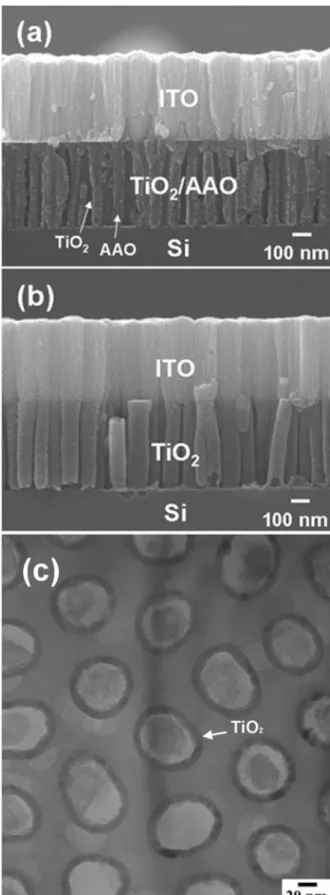
With the aid of the ALD and AAO template, self-aligned regular arrays of TiO2nanotube can be fabricated. Figures 2a and 2b show the
cross-sectional SEM images of TiO2/AAO and TiO2nanotube arrays
with ITO electrode on the top, respectively. No residual AAO template was observed in Fig. 2b and the height of TiO2nanotube array is about
600 nm. In particular, the tubular structure of TiO2 nanotube arrays
can be seen clearly in Fig. 2b. The nanotubes are vertical to the Si substrate, and have a good contact with the ITO electrode. Figure 2c show the plan-view TEM image of the TiO2nanotube arrays in the
AAO pores. The average diameter of the nanotube is about 75 nm and the wall thickness is about 8.8 nm. As shown in Fig. 2c, the gap between the neighboring TiO2 nanotubes is approximately 60 nm.
Therefore the aspect ratio of the gap is as large as 10. Therefore, the sputtered ITO film cannot fill the gap between the neighboring TiO2
nanotubes, as shown in Figure 2b.
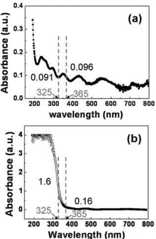
To provide the reference of the optical characteristics, the ab-sorbance measurements were performed for the AAO template layer and the TiO2 nanotube arrays fabricated on quartz substrates.
Figures 3a and 3b show the absorbance spectra of an AAO template and TiO2nanotube arrays on quartz substrates. When the wavelength
of incident light is 325 nm, the absorbance of AAO is 0.091 and the absorbance of TiO2nanotube arrays is 1.6. The absorbability of TiO2
is 17.6 times that of the AAO template. With the incident wavelength of 365 nm, the absorbance of AAO and TiO2 is 0.096 and 0.16,
re-spectively. The absorbability of TiO2 nanotube arrays is 1.66 times
that of AAO template. Therefore, TiO2nanotube arrays play a more
important role in UV absorption in the wavelength 325 or 365 nm than the AAO template.
Photoluminance was carried out to further characterize the optical properties of the TiO2nanotube arrays. Figure 4a shows the PL
spec-tra of TiO2/AAO nanotube arrays, TiO2nanotube arrays and the AAO
template on Si substrates. AAO has a bandgap of 6.2 eV.26
Theoreti-cally, a light source with the wavelength of 325 nm is not sufficient to provide energy for electrons excited from the valance band to conduc-tion band. However, it is known that the surface of AAO template is primarily amorphous aluminum oxide,27and the surface defects may
Figure 3. Absorption spectra of (a) the AAO template; and (b) the TiO2
nanotube arrays on quartz substrates.
further investigate the reason why TiO2/AAO nanotubes have
bet-ter PL emission than TiO2 nanotubes, we use Gauss fitting to
ana-lyze the sub component of the PL spectra. The PL spectrum of the AAO template is known to consist of two sub-bands: 410 nm and
the AAO surface was filled and the upper surface of AAO was cov-ered by TiO2, thus reducing the PL intensity.32On the contrary, the
PL intensity attributed from TiO2in TiO2/AAO nanotube arrays was
higher compared to TiO2only nanotube arrays. The phenomenon can
be attributed to the space confinement effect in TiO2/AAO nanotubes.
In the TiO2/AAO nanotubes case, the photogenerated electrons were
swept from the depletion region into TiO2due to the potential
gra-dient. The enhanced numbers of carriers were therefore confined in the narrow TiO2wall, which could enhance the PL intensity.34As a
result, the contribution of PL from TiO2 in TiO2/AAO nanotube
ar-rays was 5 times that of TiO2only nanotube arrays. The sub-band of
386 nm can be contributed from either TiO230, 31 or AAO.35Further
investigation at low temperatures is needed to determine the origin of these sub-bands.
TheTiO2/AAO and TiO2 nanotube arrays demonstrate different
Photoresponse behaviors. The short circuit current for the TiO2/AAO
nanotubes, TiO2nanotubes and AAO template can be obtained under
UV on/off illumination cycle when the positive electrode is connected to the ITO. The measured quantum efficiencies (QE) vs. time are shown in Figure 5. The quantum efficiency,η, is expressed as
η = the number of generated and collected electron− hole pairs the number of incident photons
= Iph/e P0/hν
= hcλeIph P0
where P0is the energy of incident UV light, h is Planck’s constant, e
is the charge of an electron,ν is the frequency of incident UV light, λ is the wavelength of incident UV light and c is the velocity of light,
Figure 4. Photoluminance spectra of (a) the
TiO2/AAO nanotube arrays, TiO2 nanotube arrays
and AAO template. Photoluminance spectra with Gauss fitting of the (b) AAO template; (c) TiO2/AAO
Figure 5. Quantum efficiency of the TiO2/AAO nanotube arrays, TiO2
nan-otube arrays and AAO template at 0 V bias under on/off UV illumination cycle.
Iphis the net photocurrent, which is the subtraction of the photocurrent
from the leakage current. The AAO template appeared irresponsive to UV illumination. However, TiO2/AAO or TiO2nanotube arrays show
a steady cycle with less than 1 sec of photoresponse time.36–38 This
special characteristic is the main reason that TiO2/AAO nanotubes
and TiO2can be used as UV detectors. Under UV illumination, the
QE obtained for TiO2/AAO nanotubes and TiO2nanotubes was 0.014
and 0.082, respectively. The conversion efficiency of TiO2nanotube
arrays is 5.86 times higher than TiO2/AAO nanotube arrays. Due to the
effect of space confinement, TiO2in TiO2/AAO nanotube arrays has
higher probability for the recombination of photo-generated electron-hole pairs resulting in better PL performance. However, it also means less electrons and holes remained in the conduction band and the
Figure 7. Energy band diagram of the ITO/TiO2/Si diode: (a) Under 0 V bias;
and (b) when positive bias is applied to the ITO electrode.
valence band, resulting in lower QE. On the contrary, TiO2nanotube
arrays have lower probability for the recombination of electron-hole pairs, but it also means more electron and holes are remained in the conduction and the valence band. As a result, TiO2has higher QE but
lower PL.
Figure 6 presents the QE results of TiO2nanotubes and TiO2/AAO
nanotubes under on/off illumination cycle at different biases. The over-all diode characteristics of ITO/TiO2/Si structures are determined by
the variation of depletion width of ITO/TiO2and TiO2/Si
heterojunc-tions. When a reverse bias is applied, the TiO2/Si heterojunction
gov-erns the photo-to-current conversion efficiency. As shown schemati-cally in Figure 7, the area of depletion region increases with a larger reverse bias, and so is the number of electron-hole pairs, as discussed in detail in previous study.39Therefore, when the bias was increased
from 0, 0.1 V to 1 V, QE of TiO2was increased from 0.082, 0.152 to
0.224, respectively. Similar trend was also observed in TiO2/AAO
nan-otube arrays, QE was increased from 0.014, 0.018 to 0.210 for bias of 0, 0.1 and 1 V, respectively. As previously mentioned, TiO2/AAO
nan-otube arrays have higher recombination effect, thus resulting in lower photo-to-current conversion performance. However, as the maximum current due to the space charge limited effect is reached,40, 41 QE of
TiO2 does not further increase with increasing bias beyond 2 V as
shown in Figure 6a. On the contrary, when the bias is larger than 2 V, QE for TiO2/AAO is 0.268, higher than QE obtained for TiO2,
as shown in Figures 6a and 6b. The phenomenon may be attributed to the following two effects. First, larger bias means TiO2/AAO is
under higher electric field. High electric field such as 4.12 MV/m at 2 V increases the transportation speed of photo-generated carriers and thus restrains the recombination of electron-hole pairs resulting from the space confinement effect. Second, there are additional elec-trons generated from the depletion region of AAO and are transported
Figure 8. Proposed energy band diagram of TiO2/AAO nanotube arrays.
Un-der UV illumination, photo-generated carriers are transported from the deple-tion region to TiO2due to the potential gradient across the nanojunction of
TiO2/AAO.
photo-carriers were discharged more easily in a short period under UV on/off illumination cycle.
Conclusions
In summary, we studied the hetero-junction effects on optical char-acteristics of TiO2nanotube arrays fabricated by ALD and AAO on Si
and quartz substrate. Due to the space confinement effect in TiO2/AAO
nanotube arrays, high probability of recombination for electron-hole pairs improves the PL intensity of TiO2 by 5 times for TiO2/AAO
nanotubes, compared with TiO2nanotubes alone. At 0 V bias,
how-ever, the space confinement effect also reduced the amount of the photo-generated electron-hole pairs remained in the conduction band and the valence band; TiO2 nanotubes therefore exhibits better QE,
in the present case, 5.8 times that of TiO2/AAO nanotube arrays.
When the bias was increased to 1 V, the TiO2nanotubes still revealed
better photon-to-electron transformation properties than TiO2/AAO
nanotubes due to the space confinement effect. However, when the bias was increased to 2 V, the high field strength would restrain the recombination phenomenon and thus increase the amount of photo-generated carriers in TiO2material. Furthermore, due to the injected
behavior of photogenerated electron from the depletion region of AAO template into TiO2 material, the number of carriers in TiO2
was enhanced further. Therefore, the quantum efficiency is improved for TiO2/AAO nanotube arrays when the biases are beyond 2 V. For
the nano-scale framework, we were successful at utilizing classical knowledge of energy band diagram to explain the photo-carriers trans-portation under UV on/off illumination.
Acknowledgments
The authors thank the National Science Council of the Republic of China, Taiwan, for the financial support in this research under Contract No. NSC-98-2221-E-009-036-MY3.
12. J. H. Park, O. O. Park, and S. Kim, Appl. Phys. Lett., 89, 163106 (2006). 13. P. Hoyer, Langmuir, 12, 141 (1996).
14. Z. Su and W. Zhou, Adv. Mater., 20, 1 (2008).
15. J. M. Macak, H. Tsuchiya, A. Ghicov, K. Yasuda, R. Hahn, S. Bauer, and P. Schmuki,
Curr. Opin. Solid State Mater. Sci., 11, 3 (2007).
16. T. Kasuga, M. Hiramatsu, A. Hoson, T. Sekino, and K. Niihara, Langmuir, 14, 3160 (1998).
17. Q. Chen, W. Zhou, G. H. Du, and L.-M. Peng, Adv. Mater., 14, 1208 (2002). 18. B. D. Yao, Y. F. Chan, X. Y. Zhang, W. F. Zhang, Z. Y. Yang, and N. Wang, Appl.
Phys. Lett., 82, 281 (2003).
19. M. S. Sander, M. J. Cˆot´e, W. Gu, B. M. Kile, and C. P. Tripp, Adv. Mater., 16, 2052 (2004).
20. A. Michailowski, D. AlMawlawi, G. Cheng, and M. Moskovits, Chem. Phys. Lett., 349, 1 (2001).
21. H. Imai, Y. Takei, K. Shimizu, M. Matsuda, and H. Hirashima, J. Mater. Chem., 9, 2971 (1999).
22. M. Adachi, Y. Murata, M. Harada, and S. Yoshikawa, Chem. Lett., 8, 942 (2000). 23. Yung-Huang Chang, Shun-Min Wang, Chien-Min Liu, and Chih Chen, Journal of
The Electrochemical Society, 157(11) K236-K241 (2010).
24. Chien-Min Liu, Chih Chen, and Hsyi-En Cheng, Journal of The Electrochemical
Society, 158(3) K58-K63 (2011).
25. C. J. Yang, S. M. Wang, S. W. Liang, Y. H. Chang, C. Chen, and J. M. Shieh, Appl.
Phys. Lett., 90, 033104 (2007).
26. S. D. Mo and W. Y. Ching, Phys. Rev. B, 57, 15219 (1998).
27. D. Routkevitch, A. N. Govyadinov, and P. P. Mardilovich, Proceedings of the ASME
Int. Mechanical Engineering Congress, MEMS, Vol. 2, Orlando (Florida), 2000,
pp. 39–44.
28. Y. Du, W. L. Cai, C. M. Mo, J. Chen, L. D. Zhang, and X. G. Zhu, Appl. Phys. Lett., 74, 2951 (1999).
29. Y. Shen, R. P. Jia, H. Q. Luo, X. G. Chen, D. S. Xue, and Z. D. Hu, Spectrochimica
Acta Part A, 60, 1007 (2004).
30. D. Li, N. Ohashi, S. Hishita, T. Kolodiazhnyi, and H. Haneda, J. Solid State Chem., 178, 3293 (2005).
31. D. Fang, K. Huang, S. Liu, and J. Huang, J. Braz. Chem. Soc., 19, 1059 (2008). 32. Y. Lei, L. D. Zhang, G. W. Meng, G. H. Li, X. Y. Zhang, C. H. Liang, W. Chen, and
S. X. Wang, Appl. Phys. Lett., 78, 1125 (2001).
33. J. M. Wu, H. C. Shih, and W. T. Wu, J. Vac. Sci. Technol. B, 23, 2122 (2005). 34. E. d. Sun, F. H. Su, Y. T. Shih, H. L. Tsai, C. H. Chen, M. K. Wu, J. R. Yang, and M.
J. Chen, Nanotechnology, 20, 445202 (2009).
35. Y. Li, C. W. Wang, L. R. Zhao, and W. M. Liu, J. Phys. D: Appl. Phys., 42, 045407 (2009).
36. A. Kongkanand, K. Tvrdy, K. Takechi, M. Kuno, and P. V. Kamat, J. Am. Chem. Soc., 130, 4007 (2008).
37. K. W. Liu, J. G. Ma, J. Y. Zhang, Y. M. Lu, D. Y. Jiang, B. H. Li, D. X. Zhao, Z. Z. Zhang, B. Yao, and D. Z. Shen, Solid-State Electron., 51, 757 (2007). 38. Y. Y. Lin, C. W. Chen, W. C. Yen, W. F. Su, C. H. Ku, and J. J. Wu, Appl. Phys. Lett.,
92, 233301 (2008).
39. Y. H. Chang, C. M. Liu, Y. C. Tseng, C. Chen, C. C. Chen, and H. E. Cheng,
Nanotechnology, 21, 225602 (2010).
40. M. Dutta and D. Basak, Appl. Phys. Lett., 92, 212112 (2008). 41. I.-S. Jeong, J. H. Kim, and S. Im, Appl. Phys. Lett., 83, 2946 (2003). 42. A. M. Cowley and S. M. Sze, J Appl. Phys., 36, 3212 (1965).