Characterisation of a suspended nanowire channel thin-film transistor with
sub-100 nm air gap
Chia-Hao Kuo
1, Chia-Wei Hsu
1, Horng-Chih Lin
1,2, Tiao-Yuan Huang
1 1Department of Electronics Engineering and Institute of Electronics, National Chiao Tung University, Hsinchu 300, Taiwan
2
National Nano Device Laboratories, Hsinchu, Taiwan
E-mail: [email protected]
Published in Micro & Nano Letters; Received on 27th February 2011; Revised on 5th May 2011
A novel suspended nanowire (NW) channel thin-film transistor (TFT) with sub-100 nm air gap has been fabricated and characterised. With a simple and low-cost over-etching-time-controlled reactive ion etching technique and a buffered-oxide etch wet-etching process, a suspended NW of 27 nm and an air gap of 10 nm were achieved. The resultant suspended-NW-channel TFTs showed an ultra-low subthreshold swing (52 mV/dec) and considerable hysteresis window (3.7 V). Finally, the impacts of device dimensions on the characteristics of suspended NW TFTs were also investigated.
1. Introduction: The CMOS-MEMS process has recently received increasing attention [1 – 3]owing to its capability to increase the functionality of IC chips. In addition to forming passive devices
[2, 3], active transistors featuring a suspended subject, such as the suspended-gate metal-oxide-semiconductor field effect transistor (SG-MOSFET) [4, 5] and nanoelectromechanical non-volatile memory (NEMory) [6], have become highly attractive for the future nanoscale low-power ICs[7]. Specifically, owing to the exist-ence of an air gap between the control gate and channel, the device depicts an extremely low-gate leakage current as it is operated in the off state [8]. In addition, unlike the conventional MOSFETs, the suspended devices utilise the mechanical switch to achieve the sub-60 mV/dec subthreshold swing (SS) at 300K[4].
However, one major issue associated with the previous works is the high operation voltage, which is typically larger than 10 V and thus not compatible with the modern CMOS circuitries. This is because of the thick air gap (.100 nm) formed in the structure. Theoretically, the operation voltage can be reduced by reducing the gap, but practically it is difficult to achieve considering the deep laterally etched structure [1 – 7]. To address the issues, a novel suspended nanowire (NW) channel device with smaller air gap was recently proposed by our group [9]. In the devices, the formation of NWs adopting the sidewall spacer-etching techniques developed by our group[10, 11] is easy without using advanced lithography such as e-beam and DUV exposure tools. Furthermore, a sub-100 nm air gap can be achieved by a simple wet-etching step. Such a thin air-gap thickness is beneficial for reducing the operation voltage. In this study, we further investigate the influences of the air-gap thickness on the characteristics of the suspended NW channel thin-film transistor (TFTs).
2. Device structures and fabrication: The top view of a completed device with major structural parameters is shown inFig. 1. Key process flows are illustrated in Figs. 2a– e, corresponding to the cross-sectional views cutting along the device centre after each specific step. The fabrication began on Si substrate capped with a thermal oxide. First, an n+doped poly-Si layer was deposited by low-pressure chemical vapour deposition (LPCVD) at 5508C and defined as the gate electrode (Fig. 2a). An SiN layer and a sacri-ficial tetraethyl orthosilicate (TEOS) oxide layer were then depos-ited, respectively, followed by the deposition of a 100 nm amorphous Si. Afterwards, a solid-phase crystallisation (SPC) treat-ment was then performed to transform the Si film from amorphous into polycrystalline phase (Fig. 2b). With a photolithography step and a reactive ion etching (RIE) step, the source/drain (S/D) regions and sidewall NWs were defined simultaneously (Fig. 2c).
Thereafter, an additional photoresist (PR) layer was covered on the channel region, followed by the phosphorous S/D ion im-plantation at 15 keV with a dose of 5× 1015cm22 (Fig. 2d). Note that the PR-covered region defines the channel length of the device, as shown inFig. 1. A 400 nm passivation oxide layer was deposited on the wafer by LPCVD at 7008C. To physically suspend the NW channels, a wet-etching process was performed to remove the sacrificial TEOS oxide layer between the NW chan-nels and the silicon nitride gate dielectric layer. As a result, an air gap was formed and the suspended NW channel TFTs were accom-plished (Fig. 2e). Fig. 3a is the scanning electron microscopic (SEM) image of a fabricated device showing the formation of the
Figure 1 Top view of the device with suspended NW channels
Figure 2 Key process flows of suspended NW channel TFT a Formation of in situ doped poly-Si gate
b Deposition of silicon nitride, TEOS anda-Si channel with SPC c Formation of S/D regions and sidewall spacer NW channels by RIE d Channel region definition and S/D implantation
e Air-gap formation
Micro & Nano Letters, 2011, Vol. 6, Iss. 7, pp. 543 – 545 543 doi: 10.1049/mnl.2011.0090
&
The Institution of Engineering and Technology 2011air gap.Fig. 3bis the transmission electron microscopic (TEM) image of the cross-sectional profile of a NW channel taken before the TEOS layer is stripped.
3. Basic electrical characteristics:Fig. 4compares transfer charac-teristics between devices with and without stripping the TEOS oxide. The devices have channel length of 1.0 mm. The original gate dielectric is composed of 30 nm oxide/20 nm nitride; therefore the nominal air gap in the suspended NW channel device is 30 nm. InTable 1, major characteristics of the two devices are summarised, and the one without stripping the TEOS oxide is denoted as the con-ventional device. In this work, threshold voltage (Vth) is defined as
the gate voltage at a drain current of 1 nA. It is seen that the sus-pended NW device exhibits much lower SS, smaller Vth, and
higher drive current (ION), even though the estimated nominal
equivalent oxide thickness (EOT) of the suspended device (128 nm) is much thicker than that of the conventional one (41 nm). These findings, together with the ultra-low SS of 52 mV/dec, which is lower than the theoretical limit of 60 mV/ dec for the conventional MOSFETs, evidence the mechanical mechanism of the suspended channel modulated by the gate bias. 4. Effects of the NW length:Figs. 5aand b show the hysteresis characteristics of the suspended NW channel devices with different channel length and S/D extension length, respectively. In these Figures, the gate voltage (VG) was first swept forward from a negative
value to a positive one, and then backward to return to the negative initial value. As has been pointed out in our previous work[9], pull-in of the NW channels is mainly triggered by the attractive
electrostatic force exerted by the applied gate voltage. However, as the central NW channels get connected with the gate nitride, additional components, such as the van der Waal force [12], become significant and should be taken into account. As a result, in the backward sweeping the NW channels tend to be pulled out and separate from the gate nitride at a voltage smaller than the pull-in one. This explains the hysteresis characteristics. InFig. 5a, for the devices with a given S/D extension length of 0.5 and 100 nm air gap, as the channel length increases from 0.4 to 5.0 mm, the Vth in the forward sweeping, hysteresis window and
the ON current all decrease accordingly. On the other hand, for the two devices shown inFig. 5bwith the same channel length (2 mm) but different S/D extension length (0.25 or 0.5 mm), the aforemen-tioned trends occur only to the one with a longer S/D extension. Since the total length of the NW is the sum of the channel and exten-sion regions, the above findings are postulated to be related to the increase in elastic constant with decreasing NW length. According Figure 3 Images of the air gap and NW channel
a SEM image of a fabricated device showing the air gap b TEM image of the cross-sectional profile of a NW channel
Figure 4 ID– VGcurves of conventional TFT and suspended-NW-channel
TFT
Table 1 Summary of the major characteristics of the conventional and suspended devices (extracted from I to V curves shown inFig. 4)
EOT, nm SS,a mV/dec Vth,b V Ion, nA I e off, pA Suspended NW Channel device 128 52 1.67 57.6c 0.12 Conventional NW Channel device 41 928 4.83 11.5d 0.34 a
Minimum value in the subthreshold regime
b
Defined as the VGat drain current of 1 nA c Extracted at VGof 4 V dExtracted at V Gof 8 V e Extracted at VGof 0 V
Figure 5 Hysteresis curves of the suspended-NW-channel TFTs a With channel length of 0.4, 1 and 5 mm, respectively b With S/D extension length of 0.25 and 0.5 mm, respectively
544 Micro & Nano Letters, 2011, Vol. 6, Iss. 7, pp. 543 – 545
to one previous work[12], elastic constant is inversely proportional to the cubic power of the length of the suspended subject. Therefore for a device with a shorter channel length or S/D extension length, it needs a larger electrically attractive force to overcome the elastic force. This leads to a larger Vthas observed in these Figures.
InFig. 5b, the one with extension length of 0.25 mm presents a lower ON current, although its total NW length is longer than the other device characterised in this Figure. As has been pointed out in our previous work[9], the contact of the NW channel with the gate nitride during operation occurs mainly in the channel centre, rather than the whole channel. The above difference in the two devices can thus be attributed to the reduced length of the 2 mm-long undoped suspended channels in contact with the gate nitride in the ON state for the device with shorter (0.25 mm) S/D extension. An air gap remains in the isolated NW regions, resulting in a larger EOT and thus limiting the drive current.
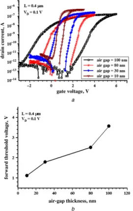
5. Effects of the air gap: Impacts of the air-gap thickness on device performance are exhibited inFig. 6a, where devices with four differ-ent air-gap thicknesses (10, 30, 80 and 100 nm) are characterised and compared. Clearly, the air-gap thickness strongly affects the electrical characteristics of the devices with suspended NW channels. A thinner gap corresponding to a smaller electrostatic force attracting the sus-pended channels results in smaller VG, as shown in Fig. 6b.
Besides, smaller displacement of NWs leads to a smaller elastic recovery force causing easier occurrence of the pull-out process, that is, a larger Vthin the reverse sweeping. This implies the hysteresis
window generally increases as the gap thickness increases. Compared with the SG-FET with high pull-in voltage (.10 V)[13], the sus-pended-NW-channel devices with sub-100 nm gap thickness indeed depict a much reduced threshold voltage (e.g. 1.11 V for tgap¼ 10 nm), which is compatible with modern CMOS circuitries.
This is attributed to the reduction in initial air-gap thickness as well as the use of tiny NW as the suspended object.
6. Conclusion: In this study, we characterised a novel suspended-NW-channel device with major attention paid to the effects of device structural parameters. As compared with the case without an air gap, superior characteristics including steeper SS and lower Vthare achieved with the proposed devices. We have also studied
how the geometric structural dimensions such as channel length, S/D extension length, and air gap affect the device characteristics. These results show that, as the air gap is shrunk below 100 nm, the proposed device with a small Vth compatible with modern
CMOS circuitries is feasible.
7. Acknowledgments: The authors would like to thank the staff of National Nano Device Laboratories (NDL) and the Nano Facility Center (NFC) of the NCTU for assistance in device fabrica-tion. This work was supported in part by the National Science Council under contract No. NSC 99-2221-E-009-167-MY3. 8 References
[1] Colinet E., Durand C., Audebert P., et al.: ‘Measurement of nano-displacement based on in-plane suspended-gate MOSFET detection compatible with a front-end CMOS process’, IEEE J. Solid-State Circuits, 2009, 44, (1), pp. 247 – 257
[2] Qu H., Xie H.: ‘Process development for CMOS-MEMS sensors with robust electrically-isolated bulk silicon microstructures’, J. Microelectromech. Syst., 2007, 16, (5), pp. 1152 – 1161
[3] Xie H., Fedder G.K.: ‘Fabrication, characterization, and analysis of a DRIE CMOS-MEMS gyroscope’, IEEE Sens. J., 2003, 3, (5), pp. 622 – 631
[4] Abele´ N., Fritschi R., Boucart K., Casset F., Ancey P., Ionescu A.M.: ‘Suspended-gate MOSFET: bringing new MEMS functionality into solid-state MOS transistor’. IEDM Tech. Dig., 2005, pp. 1075 – 1077
[5] Abele´ N., Villaret A., Gangadharaiah A., Gabioud C., Ancey P., Ionescu A.M.: ‘1T MEMS memory based on suspended gate MOSFET’. IEDM Tech. Dig., 2006, pp. 234 – 237 [6] Choi W.Y., Kam H., Lee D., Lai J., Liu T.J.K.: ‘Compact
nanoelectro-mechanical non-volatile memory (NEMory) for 3D integration’. IEDM Tech. Dig., 2007, pp. 603 – 606 [7] Pruvost B., Mizuta H., Oda S.: ‘3D design and analysis of
functional NEMS-gate MOSFETs and SETs’, IEEE Trans. Nanotechnol., 2007, 6, (2), pp. 218 – 224
[8] Kam H., Lee D., Howe R., King T.-J.: ‘A new nano-electromechanical field effect transistor (NEMFET) design for low-power electronics’. IEDM Tech. Dig., 2005, pp. 463 – 466
[9] Lin H.C., Kuo C.H., Li G.J., Su C.J., Huang T.Y.: ‘Operation of a novel device with suspended nanowire channels’, IEEE Electron Device Lett., 2010, 31, pp. 384 – 386
[10] Lin H.C., Lee M.H., Su C.J., Huang T.Y., Lee C.C., Yang Y.S.: ‘A simple and low-cost method to fabricate TFTs with poly-Si nanowire channel’, IEEE Electron Device Lett., 2005, 26, (9), pp. 643 – 645
[11] Lin H.C., Su C.J.: ‘High-performance poly-Si nanowire NMOS transistors’, IEEE Trans. Nanotechnol., 2007, 6, (2), pp. 206– 212 [12] Akarvardar K., Eggimann C., Tsamados D., et al.: ‘Analytical modeling of the suspended-gate FET and design insights for low-power logic’, IEEE Trans. Electron Devices, 2008, 55, (1), pp. 48 – 59
[13] Bardon M.G., Neves H.P., Puers R., Van Hoof C.: ‘Scaling the suspended-gate FET: impact of dielectric charging and roughness’, IEEE Trans. Electron Devices, 2010, 57, (4), pp. 804 – 813
Figure 6 Impacts of the gap thickness on the fabricated devices with four different NW thicknesses
a Hysteresis curves of the suspended NW channel TFTs with gap thickness of 100, 80, 30 and 10 nm, respectively
b Plot of forward Vthagainst gap thickness for the suspended NW channel
TFTs
Micro & Nano Letters, 2011, Vol. 6, Iss. 7, pp. 543 – 545 545 doi: 10.1049/mnl.2011.0090