ISSN:1369 7021 © Elsevier Ltd 2011 DECEMBER 2011 | VOLUME 14 | NUMBER 12
6 0 8
Since the 1990s, portable electronic products have been a prominent part of our daily lives; and many of these devices require flash memories. The floating-gate (FG) structure, invented by Sze and Kahng at Bell Labs in 1967, forms the primary technology necessary to construct flash memories 1, Fig. 1a. In order to meet the demands of product miniaturization, the shrinking of transistors has evolved as a method to not only pack more devices into a given area, but also improve the switching speed. In such a situation, conventional nonvolatile memory (FG) suffers from certain physical limitations, such as an insufficient tunneling oxide thickness from the continual scaling down of the device structure s2. Because the floating gate (as a
charge storing layer) is conductive, all charge will be lost if a leakage path appears in the tunneling oxide, resulting in a serious reliability issue for memory applications. Discrete nanocrystal memory was first proposed by IBM in 1995, and by the early 2000s researchers were already considering it to be a promising candidate for the solution of the scaling probl em3 (Fig. 1b). In addition, nanocrystal memory has a two bit per cell storage capability due to its discrete electron storing center. This means that more data can be stored in one memory cell, which readily increases the memory dens ity4.
In nanocrystal memory, information is stored in the nanocrystals by injecting (removing) charges; therefore a transistor needs larger
Flash nonvolatile memory has been widely applied in portable electronic
products. However, traditional flash memory is expected to reach
physical limits as its dimensions are scaled down; the charges stored
in the floating gate can leak out more easily through a thin tunneling
oxide, causing a serious reliability issue. In order to solve this problem,
discrete nanocrystal memory has been proposed and is considered to be
a promising candidate for the next generation of nonvolatile memories
due to its high operation speed, good scalability, and superior reliability.
This paper reviews the current status of research in nanocrystal
memory and focuses on its materials, fabrication, structures, and
treatment methods to provide an in-depth perspective of state-of-the-art
nanocrystal memory.
Ting-Chang Changa,*, Fu-Yen Jiana,b, Shih-Cheng Chenc, and Yu-Ting Tsaib
aDepartment of Physics, National Sun Yat-Sen University, Kaohsiung, 804, Taiwan, R.O.C.
bDepartment of Electronics Engineering & Institute of Electronics, National Chiao Tung University, Hsinchu, Taiwan 300, R.O.C. cDepartment of Electrical Engineering & Institute of Electronic Engineering, National Tsing Hua University, Taiwan, R.O.C.
*E-mail: [email protected]
(smaller) voltage to turn it on, called the program (erase) operation (Fig. 1c). The digital “0” or “1” memory status is determined by applying a read voltage (Vread) to the gate between the program
and erase operations to read the corresponding drain current. Fowler-Nordheim (FN) tunneling and channel hot electron injection (CHEI) are the two most commonly employed mechanisms for the program operation, and FN tunneling for the erase operation5. FN
tunneling is a phenomenon through which electrons can easily tunnel through a triangular barrier induced by a high gate field. The CHEI mechanism is the process through which an electron gains energy from an electric field (near drain) and then collides with the lattice to redirect it into the charge storage layer. An appropriate threshold voltage shift, high memory density, low power consumption, as well as superior retention and endurance properties are thus necessary for an advanced nonvolatile memory. Nanocrystal flash memory has now been demonstrated commercially, such as in Freescales’s 90 nm node embedded nanocrystal flash memory and 128KB NOR split gate nanocrystal memory, and Numonyx’s 4 MB nanocrystal me m ory6-8.
This review provides a complete and thorough study of nanocrystal memory technologies that can compatibly combine with the integrated circuit (IC) industry. If nanocrystal memory follows industry-compatible IC techniques, it will be possible to rapidly commercialize nanocrystal memory devices. In this article, we review how nanocrystal materials, device structures, and nanocrystal fabrication processes influence the properties of nanocrystal memory and discuss the challenges that lie ahead.
Nanocrystal formation methods
Generally, a metal-oxide-nanocrystal-oxide-silicon nonvolatile memory structure is fabricated as follows. First, a silicon (100) wafer is cleaned by the Radio Corporation of America (RCA) standard cleaning process, which removes the native oxide and micro-particles from the wafer surface. A high quality oxide layer of 5 nm thickness is then grown as
a tunneling oxide. Afterwards, a charge trapping layer is deposited, and then, depending on the material, a treatment (e.g., primarily thermal) may be necessary to produce nanocrystals. Next, a thick oxide layer is deposited to serve as a blocking oxide. Finally, gate electrodes are deposited and patterned. The process flow and the structure of the memory are shown in Fig. 2.
There are numerous methods that can be used to form nanocrystals as storage centers for nonvolatile memory applications. The most commonly used are self-assembly, precipitation, and chemical reaction, as described below9-11:
Self-assembly
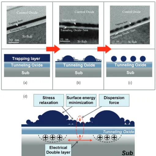
The basic procedures of self-assembly for nanocrystal formation are shown in Figs. 3a-c. A trapping layer of 1 – 5 nm is deposited and then the film is annealed at a temperature close to its eutectic temperature in an inert ambient gas to transform the trapping layer into a nanocrystal structure. The diameter of the nanocrystal is influenced by the thickness of the trapping layer, as well as the temperature and duration of the thermal treatment. Fig. 3d illustrates the major driving forces that contribute to this process. Dispersion forces and the electrical double layers affect the nanocrystal size and location distrib utions12-14. This
process is accomplished through the relaxation of film stress and is limited by the surface mobility. During the thermal treatment, these atoms gain enough surface mobility, allowing the film to self-assemble into the more thermodynamically and energetically stable state. The film breaks into “islands” along the initial perturbation to reduce the elastic energy carried by the stress built into the film during the deposition process. Moreover, minimization of the surface energy and the dispersion force between the top and bottom interfaces is conducive to stabilizing the film. Therefore, the final geometry depends on the balance between
Fig. 2 Process flow and structure of nanocrystal nonvolatile memory.
(a) (b)
(c)
Fig. 1 (a) Floating gate nonvolatile memory structure. (b) Nanocrystal nonvolatile memory structure. (c) Program and erase mode of the nanocrystal memory device.
(a) Pre-gate RCA cleaning & tunneling Oxide deposition
(b) Trapping layer deposition
(c) Transform trapping layer to nanocrystal structure
(d) Blocking oxide deposition
(f) Source and Drain implantation and activation
(e) Gate deposition and gate patterning
DECEMBER 2011 | VOLUME 14 | NUMBER 12 6 1 0
these driving forces. The forces between those regions helps stabilize the nanocrystals and keep a uniform distance between them. However, using self-assembly for nanocrystal formation cannot ensure that the trapping layer is completely discrete.
Precipitation
An oversaturated or mixed trapping layer is prepared by ion implantation into a deposited insulator layer or co-deposit system to form nanocrystals by further thermal annealing. The nucleation of nanocrystal formation during rapid thermal annealing (RTA) process can be described as following. Initially, oversaturated solid-solutes separate during thermal annealing. As the temperature and duration of the thermal annealing increases, these educts can obtain enough energy to leave their initial sites and diffuse through the mixed film. Educt diffusions with a large enough number of collisions will result in nuclei fo rmation15. With the
increase in annealing temperature, more educts tend to bond to the nuclei and form the nanocrystal structure in the trapping layer, forming a high density distribution of nanocrystal structures, as shown in Fig. 4. However, employing traditional high-energy ion implantation for nanocrystal
memory applications has revealed some obvious shor tcomings16-17. The
ion distribution (following a Gaussian distribution) is wide with high injection energy (~30 – 150 keV), such that controlling the nanocrystals close to the tunneling oxide is difficult. In addition, even when the implanted ion reaches the interface between the silicon oxide and silicon substrate, it may cause damage to the tunneling oxide, resulting in degradation of the device performance.
Chemical reaction
The chemical reaction method is widely used to form a nanocrystal trapping layer and is illustrated in Fig. 5. Initially, a binary or tertiary mixed layer is co-deposited by different material systems, and then the layer is oxidized by RTA under an oxygen flow. Different materials have different oxidation capabilities due to their different Gibbs free e nergies18-34; it is easier to form
a stable oxide compound when it has lower enthalpy. Therefore, during RTA oxidation, one material comprising the binary mixed layer is typically more easily oxidized while the other material tends to conjugate with other atoms of the same material to form the nanocrystal. A similar process also occurs for the tertiary mixed layer.
Fig. 3 TEM image and schematic drawing of nanocrystal formation by self-assembly with increased duration of thermal treatment from (a) to (c); the trapping layer was deposited by reactive sputtering of a Ni target in an Ar and N2 environment at room temperature. (d) Major driving forces in nanocrystal formation by self-assembly. © 2002 IEEE. Reprinted, with permission, from12.
(a) (b) (c)
In order to form the nanocrystal and the surrounding oxide, oxygen and heat are both key factors. Oxygen can not only be introduced into the mixed layer at the co-depositing stage but also during the RTA process for better oxygen concentration control. The control of the oxygen concentration in the mixed layer is an important issue. A low oxygen concentration causes insufficient oxidation of the mixed layer and higher leakage current. A high oxygen concentration can result in the oxidation of the nanocrystal. The memory property can be lost if either of these two conditions occur.
Of the methods described above, both research and practical experience support precipitation and chemical reaction as the best methods of forming nanocrystals for a mixed material trapping layer, because it is easier to control the size and density of the nanocrystals.
The evolution of materials and technology
Currently, nanocrystal nonvolatile memory can be classified into three major categories, determined via the materials used: (i) semiconductor, (ii) metal, and (iii) high-κ dielectric nanocrystals. Since silicon (Si) and germanium (Ge) are fully compatible with the semiconductor industry, nanocrystal memory based on Si and Ge have been extensively inv estigated5,35-40. Silicon nanocrystal memory was
first introduced as a replacement for the conventional floating gate in the non-volatile memory (NVM) structure by Tiwari et al. in the
early 1990s35. It seems promising to use Ge nanocrystals rather than
Si nanocrystals because of their higher dielectric constant (∼16.0) and smaller band gap (~0.6 eV). Chen et al. proposed that Ge nanocrystals have a strong coupling with the conduction channel, and that a large memory window under low program/erase voltages coul d be achieved41. Moreover, Shi’s model of nanocrystal memory indicated
that the injected charges are mainly stored on the deep trapping centers, resulting in long-term charge storage42. Recently, Ge/Si
hetero-nanocrystal memories were demonstrated by Shi’s group43 for
the first time, as a replacement for the conventional floating gate in non-volatile memory (NVM) structures. Hetero-nanocrystal memory can enhance device performance; lengthening retention time, speeding up programming speed, and raising the charge storage capability, when compared with Si nanocrystal memory. This is due to the fact that an Si interface around the Ge nanocrystal increases barrier height between the Ge/Si interface and prevents the stored nanocrystal charges fr om leaking out43,44. In addition, a core-shell Ge-Si nanocrystal structure
has also been proposed to improve the nanocrystal-insulator interface quality, resulting in better device performance characteristics, such as improved retention time and program ming/erasing speed45.
In optimizing nanocrystal NVM devices, the ideal goal is to simultaneously achieve fast DRAM program/erase speeds and long flash memory retention times. For this purpose, we must create an asymmetry in charge transport through the gate dielectric to maximize the IG, program/erase/IG, retention ratio. One approach for achieving this goal is to engineer the depth of the potential well at the storage nodes, thus creating a large energy band offset between the Si substrate and the storage nodes for programming and retention operations. This can be achieved if the storage nodes are made of metal nanocrystals. The major advantages of metal nanocrystals over semiconductor nanocrystals include: (i) higher density of states around the Fermi level (ii) scalability of the nanocrystal size (iii) a wide range of available work functions and (iv) smaller energy perturbations due to carrier confinement12.
In addition, electrostatic modeling (from both analytical formulation and numerical simulation) has demonstrated that metal nanocrystals significantly enhance the electric field between the nanocrystal and the sensing channel set up by the control gate bias, and hence such a system can achieve a much higher efficiency in low-voltage prog ram/erase operations46.
Numerous attempts have been made to improve NVM device performance and reliability using metal nanocrystals. Liu et al. reported the growth of Au, Pt, and Ag nanocrystals on SiO2 using an
e-b eam deposition method12. Yang and Hu et al. proposed Ni and
Co nanocrystals and a high-κ di electric NVM structure47-49. Metallic
silicide nanocrystals have also been developed, due to the fact that metallic silicide nanocrystals are easy to fabricate and have good thermal stability compared wi th metal nanocrystals50-52.
High-κ dielectric nanocrystal nonvolatile memories (HfO2 and
CeO2 nanocrystals embedded in SiO2) were first propos ed by Lin and
Fig. 5 Schematic drawing of nanocrystal formation by chemical reaction. Fig. 4 Schematic drawing of nanocrystal formation by precipitation.
DECEMBER 2011 | VOLUME 14 | NUMBER 12 6 1 2
Yang et al.53-54.Hf and Si were co-sputtered in oxygen followed with
high-temperature annealing to form high-κ dielectric nanocrystals. These devices exhibited very little lateral or vertical stored charge migration
after an endurance test. These features suggest that such cells could be very useful for high-density two-bit nonvolatile memory applications.
From the consideration of the Gibbs free energy, thermodynamics indicates that it is easier for Si to be oxidized than a metal during the rapid thermal oxidation (RTO) process. Due to the lower oxidation free energy of SiO2, metal nanocrystals easily precipitate into an SiO2
dielectric layer from a metal and silicon mixed layer. Therefore, the peak RTO temperature of nanocrystal formation decreases with an increase in the Gibbs free energy of a metal oxide compound, as shown in Table 118-33, 44. The larger the difference between the Si-O Gibbs
free energy, the lower the RTO temperature that is required for metal nanocrystal formation. The RTO temperature is an important factor in the thermal budget for compatibility with CMOS methods: metal nanocrystals with lower formation temperatures are preferable for application in standard CMOS processes.
An alternative approach is to engineer the depth of the potential well (deff) at the storage nodes, which could be achieved by selecting suitable metal materials by considering the metal work function. An asymmetrical barrier is created between the substrate and the storage
Table 1 Gibbs free energy and corresponding RTA
temperatures of various materials
Element bond Gibbs free energy (kJ mol-1) RTA temperature (˚C)
Ag-O -220.1 ± 20.9 500~550 Au-O -221.8 ± 20.9 600~650 Ni-O -382.0 ± 16.7 500~550 Co-O -384.5 ± 13.4 500~550 Pt-O -391.5 ± 41.8 900~950 Al-O -511 ± 3 N/A Mo-O -560.2 ± 20.9 900~950 Ge-O -659.4 ± 12.6 900~950 W-O -672.0 ± 41.8 900~1100 Si-O -799.6 ± 13.4 N/A
Fig. 6 Energy band diagram for metal nanocrystals embedded between a control oxide and tunnel oxide during (a) programming and (b) retention. (c) Work functions of various nanocrystal materials.
(a) (b)
(c)
Table 2 Work functions and corresponding memory
characteristics of various materials
Element Tunnel
dielectric Sweep voltage (V)
Memory windows (V) Reference Si SiO2 10 to -10 4.6 Ref. 10 Ge SiO2 5 to -5 0.42 Ref. 55 Au SiO2 2 to -4 2.3 Ref. 56 Ag SiO2 2 to -4 2.1 Ref. 56 Pt SiO2 2 to -4 3.8 Ref. 56 W SiO2 10 to -10 9 Ref. 58 Ni SiO2 10 to -10 4 Ref. 57 HfO2 2 to -2 0.75 Ref. 56
NiSi SiO2 3 to -3 1.04 Ref. 56
HfO2 3 to -3 1.38 Ref. 56
Co SiO2 7 to -7 1.8 Ref. 48
CoSi2 SiO2 3 to -3 1.1 Ref. 56
Mo SiO2 9 to -11 3.6 Ref. 59
Al AlN 5 to -5 1 Ref. 56 Ni1-xFex PI 11 to -6 2 Ref. 56
TiN Al2O3 16 to -16 2.9 Ref. 22
HfO2 SiO2 Vg =9V, Vd=9V 2.2 Ref. 21
nodes, i.e., a small barrier for programming and a large barrier for retention. During the program process, the charges need to overcome the energy barrier of the tunneling oxide, as shown in Fig. 6a. For retention, the asymmetrical barrier structure provides the extra energy barrier height (deff) to prevent the stored charges escaping
from the storage nodes through the oxide, as shown in Fig. 6b. The memory effects of Ag, Au, Pt, W, Co, Ni, NiSi2, Ni1-xFex, Hf, TiN, and
Al metal nanocrystals have all been f abricated and studied18-33,44. An
improved memory effect can be observ ed when deff is higher18-20,44.
The relationship between the metal work function and the silicon energy band is shown in Fig. 6c; such a diagram can be used to assist researchers in determining the appropriate metal. Furthermore, a summary of research findings on using various metal nanocrystals as charge storage no de s ca n be found in Table 210,21,22,48,55-60.
The semiconductor (Si-base) NC-NVM is compatible with the integrated circuit industry; the source of the earliest research and the most mature fabrication technology. High-κ dielectric NC-NVM devices can restrain the stored charge migration after an endurance test.
Further, such cells could be useful for high-density two-bit nonvolatile memory applications. In metal NC-NVM fabricated technology, the program efficiency and data retention can be improved by engineering an asymmetrical barrier structure. Also, the NC formation oxidation temperature can be reduced by the metal/silicon mix.
The evolution of device structure
Good nonvolatile memory should exhibit a high program/erase speed, low power consumption, a sufficient memory window, and superior reliability (endurance and retention). A number of approaches for improving memory properties have been proposed and demonstrated. However, these approaches are often a trade-off between memory performances such as the program/erase speed and the retention time. By scaling down the tunneling oxide, for example, the program/erase speed can be increased, but results in the degradation of the retention property. Some approaches have thus been introduced to improve the program/erase speed and/or retention time without sacrificing other memory properties. These approaches include tunneling barrier engineering, multi-layer nanocrystals, work function engineering, and surrounding oxide passivation.
The concept of tunneling oxide engineering is based on an asymmetric energy barrier in the tunneling oxide, which is dependant on the memory status, which is either in program/erase or retention mode. Generally, the barrier height (φ) of conventional tunnel oxide is not influenced by the gate voltage, regardless of whether the system is in program/erase status or in retention status, as shown in Fig. 7a. S. Baik et al. proposed a nitride-oxide-nitride structure with an adjustable barrier height to improve the program/erase speed61. This
adjusted tunneling oxide barrier height (jφ′) is lowered during program operation when a positive voltage is applied on the gate, as shown by the dashed line in Fig. 7b. Thus it is easier for electrons to be injected from the substrate into nanocrystals. After the program operation, the energy barrier returns to its original height to prevent electrons tunneling from the nanocrystals back to the substrate during retention status, shown as the solid line in Fig. 7b. In addition, nanocrystal memory with an asymmetric SiO2/HfO2 structure has been proposed based
on a modifiable barrier width62,63. The barrier width of SiO 2/HfO2
is thinner than that of a single oxide layer when a sufficient positive voltage is applied to the gate for programming, as shown in Fig. 7c.
During retention, the barrier keeps its original width to prevent the electron tunneling from the nanocrystals back to the substrate, as shown in Fig. 7d. Using these tunneling oxide engineering approaches, the program/erase speed can be improved without sacrificing retention time.
A multi-layer nanocrystal approach of improving memory retention has been propose d by R. Ohba and W. R. Chen et al.41,64,65. As shown in
Fig. 7e, lower-layer nanocrystals can suppress the charge leakage from upper-layer nanocrystals into the substrate by the Coulomb blockade effect. Therefore, multi-layer nanocrystal memory can achieve a better charge storage ability than typical single-layer nanocrystal memory.
(a) (b)
Fig. 7 Energy band diagrams of (a) a conventional tunnel oxide, (b) a nitride-oxide-nitride structure, (c) a SiO2/HfO2 structure during programming, (d) a SiO2/HfO2 structure during retention status, and (e) a multi-layer nanocrystal.
(c) (d)
DECEMBER 2011 | VOLUME 14 | NUMBER 12 6 1 4
The work function engineering approach in metal nanocrystals, based on an asymmetrical barrier between the substrate and a deep potential well, has been fully discussed in the previous section. For metal nanocrystal memory, a smaller energy barrier during program operation and a large r one during retention can be achieved14, as
shown in Figs. 6a,b. Therefore, the program/erase speed and retention time can be simultaneously improved.
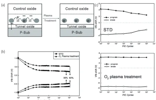
Finally, memory properties can be significantly improved by enhancing the quality of the oxide surrounding the nanocrystals. After treatment of the surrounding oxide, the charge leakage though that oxide can be effectively suppressed, both during program/erase status and retention status, as shown in Fig. 8. Thus the memory window and program/erase speed, as well as retention and endurance properties, can be improved. S. C. Chen et al. proposed a plasma treatment method to improve memory properties. The Si dangling bonds in the oxide surrounding the nanocrystals can be passivated by plasma treatments66, 67, resulting
in a superior memory window and retention time. In addition, the experimental results reveal that the endurance is also improved after plasma treatment as the result of the superior oxide quality. Other methods, such as the s upercritical fluid CO2 (SCCO2) technique68- 71, can
also be used to enhance the oxide quality. After SCCO2 treatments, the traps in the oxide are passivated, and thus the leakage current through traps (i.e., trap-assisted tunneling) can be effectively suppressed.
Challenges
Although nanocrystal memory possesses many advantages and is considered a promising candidate for the solution to the scaling problem in conventional floating gate memory, there are still some challenges that must be overcome.
Reproducibility
Nanocrystal memory properties are influenced by nanocrystal size, shape, and configuration. Nanocrystals are not formed by patterning, hence fluctuations bet ween individual devices becomes important72.
According to the International Technol ogy Roadmap for Semiconductors (ITRS 2009)73, memory cell size is likely to reduce to 1000 nm2 by
2020. This means that only about ten nanocrystals can be contained in every memory cell. On such a small scale, it becomes increasingly challenging to synthesize suitable materials with uniform size and shape, and assemble them into a well-ordered nanocrystal matrix74.
Charge leakage
High density nanocrystals can store more charge in a memory device and mitigate the influence of fluctuations between individual devices because there are more nanocrystals in each memory cell. However, the charges stored in nanocrystals leak though the surrounding oxide more easily in high density nanocrystal systems. If the surrounding oxide cannot effectively prohibit the charge transport between nanocrystals, nanocrystal memory will lose the advantage of having a discrete charge storage node; that is, preventing the loss of total stored charge through a leakage path in the tunnel oxide. Even though surrounding oxide passivation can alleviate the charge transport between nanocrystals, eventually the charges in nanocrystals will directly tunnel through the thin surrounding oxide if the nanocrystal density continues to increase.
Summary
Conventional FG memory faces the limitation that all stored charge will leak back to the channel through a path formed by repeated operation.
Fig. 8 (a) After surrounding oxide treatment, charge leakage though the surrounding oxide can be effectively suppressed. (b) The retention and (c) endurance characteristics of the memory improved after the surrounding ox ide treatment. Reprinted with permission from66. © 2010, Elsevier.
(c) (a)
To alleviate the trade-off of tunnel oxide design for FG memory devices, memory-cell structures employing discrete traps as charge storage media have been proposed in the past few years. In this paper, we have introduced three of the most commonly used methods of fabricating nanocrystal structures: self-assembly, precipitation, and chemical reaction. We suggest that precipitation and chemical reaction are the two best methods for forming a uniform and easy-controllable discrete nanocrystal structure. This paper also reviews the three major nanocrystal materials: semiconductors, metals, and high-κ dielectric nanocrystals, and discusses the impact of each technology on the memory characteristics. Metallic nanocrystals are considered the most promising for commercial production. In addition, in order to simultaneously achieve high program/erase speeds and long retention
times without sacrificing other memory properties, tunneling barrier engineering, multi-layer nanocrystals, work function engineering, and surrounding oxide passivation have been proposed. However, nanocrystal memory still faces some challenges upon scaling down, such as fluctuations from device to device and charge leakage at high density. It is, therefore, important to continue to find methods that strategically match the scaling limits with appropriate requirements in the NVM industry.
Acknowledgements
The work was supported by the National Science Council under Contract Nos. NSC 100-2120-M-110-003, NSC99-2120-M-110- 001 and NSC-97-2112-M-110-009-MY3.
REFERENCES
1. Kahng, D., and Sze, S. M., Bell Syst Tech J (1967) 46, 1288.
2. Maes, H. E., et al., Trends in non-volatile memory devices and technologies,
Presented at Proc. 17 European Solid State Devices Res. Conf., Bologna, 1987. 3. Tiwari, S., et al., Appl Phys Lett (1996) 68, 1377.
4. Liu, Z., et al., IEEE Trans Electron Devices (2002) 49, 1614.
5. Blauwe, J. D., IEEE Trans Nanotechnol (2002) 1, 72. 6. Muralidha, R., et al., IEEE ICICDT (2004) 31. 7. Chindalore, G., et al., IEEE VLSI Tech (2008) 136.
8. Gera, C., et al., IEEE IEDM (2008) 1.
9. LEE, C., et al., J Electronic Mater (2005) 34, 1.
10. Kapetanakis, E., et al., Appl Phys Lett (2000) 77, 3450. 11. Chen, C. H., et al., Appl Phys Lett (2008) 92, 013114. 12. Liu, Z., IEEE Trans Electron Devices (2002) 49, 1606. 13. Suo, Z., and Zhang, Z., Phys Rev B (1998) 58, 5116. 14. Bonnell, D. A., et al., Acta Mater (1998) 46, 2263. 15. Hu, C. W., et al., J Electrochem Soc (2009) 156, H751. 16. Borany, J. V., et al., Solid State Electron (1999) 43, 1159. 17. Park, C. J., et al., Appl Phys Lett (2006) 88, 071916. 18. Lee, C., et al., IEDM Tech Dig (2003) 557. 19. Tseng, J. Y., et al., Appl Phys Lett (2004) 85, 2595. 20. Takata, M., et al., IEDM Tech Dig (2003) 553. 21. Lin, Y. H., et al., IEEE Electron Device Lett (2005) 26, 154. 22. Choi, S., et al., Appl Phys Lett (2005) 86, 123110. 23. Liu, Y., et al., Appl Phys Lett (2005) 87, 033112. 24. Tan, Z., et al., Appl Phys Lett (2005) 86, 013107. 25. Lee, J. J., et al., Appl Phys Lett (2005) 86, 103505.
26. Lee, J. J., and Kwong, D. L., IEEE Trans Electron Devices (2005) 52, 507. 27. Yeh, P. H., et al., Appl Phys Lett (2005) 87, 193504.
28. Yeh, P. H., et al., J Vac Sci Tech A (2005) 23, 851. 29. Kim, J. H., et al., Appl Phys Lett (2005) 86, 032904. 30. Paul, S., et al., Nano Lett (2003) 3, 533.
31. Chandra, A., and Clemens, B. M., Appl Phys Lett (2005) 87, 253113. 32. Liu, Z., et al., IEEE Trans Electron Devices (2003) 24, 345. 33. Kouvatsos, D. N., et al., Appl Phys Lett (2003) 82, 397. 34. Chen, J. H., et al., IEEE Trans Electron Devices (2004) 51, 11. 35. Tiwari, S., et al., IEDM Tech Dig (1995) 521.
36. Chang, T. C., et al., Electrochem Solid State Lett (2005) 8, 71. 37. Hanafi, H. I., et al., IEEE Trans Electron Devices (1996) 43, 1553.
38. Choi, W. K., et al., Appl Phys Lett (2002) 80, 2014. 39. Tu, C. H., et al., Appl Phys Lett (2006) 89, 052112. 40. Chen, W. R., et al., Appl Phys Lett (2009) 91, 102106. 41. Chen, W. R., et al., IEEE Trans Electron Devices (2009) 8, 185. 42. Shi, Y., et al., J Appl Phys (1998) 84, 2358.
43. Shi, Y., et al., First Joint Symposium on Opto- and Microelectronic Devices and
Circuits, Nanjing, China. (2000) 142.
44. Yang, H. G., et al., Microelectron (2003) 34, 71. 45. Liu, H., et al., IEEE Trans Electron Devices (2008) 55, 3610. 46. Lee, C., et al., IEEE Electron Device Lett (2005) 26, 879. 47. Yang, F. M., et al., Appl Phys Lett (2007) 90, 222104. 48. Yang, F. M., et al., Appl Phys Lett (2007) 90, 132102. 49. Hu, C. W., et al., Appl Phys Lett (2009) 94, 102106. 50. Zhu, Y., et al., Appl Phys Lett (2006) 88, 103507. 51. Zhu, Y., et al., Appl Phys Lett (2006) 89, 233113. 52. Li, B., et al., Appl Phys Lett (2010) 96, 1721043. 53. Lin, Y. H., et al., IEDM Tech Dig (2004) 1080. 54. Yang, S. M., et al., IEDM Tech Dig (2008) 48.
55. Chang, T. C., et al., Electrochem Solid State Lett (2004) 7, G17. 56. Yeh, P. H., et al., Electrochimica Acta (2007) 52, 2920. 57. Hu, C. W., et al., Electrochem Solid State Lett (2010) 13, H49. 58. Chen, S. C., et al., Thin Solid Films (2010) 519, 1677. 59. Lin, C. C., et al., Appl Phys Lett (2008) 93, 222101. 60. YANG, S. M., et al., Jap J Appl Phys (2007) 46, 3291. 61. Baik, S., et al., IEDM Tech Dig (2003) 545. 62. Seol, K. S., et al., Appl Phys Lett (2006) 89, 083109. 63. Lu, J., et al., Appl Phys Lett (2010) 96, 262107
64. Ohba, R., et al., IEEE Trans Electron Devices (2002) 49, 1392. 65. Chen, W. R., et al., J Appl Phys (2008) 104, 094303. 66. Chen, S. C., et al., Thin Solid Films (2010) 518, 7339 67. Chen, S. C., et al., Thin Solid Films (2011) 519, 3897 68. Tsai, C. T., et al., J Appl Phys (2008) 103, 6.
69. Tsai, C. T., et al., Electrochem Solid State Lett (2009) 12, H35. 70. Chen, M. C., et al., Appl Phys Lett (2009) 94, 162111. 71. Chen, C. H., et al., Appl Phys Lett (2007) 91, 232104. 72. Steimle, R. F., et al., Microelectron Reliab (2007) 47, 585.
73. International Technology Roadmap for Semiconductor Industry (ITRS) 2009 Update, Interconnet San Jose, CA (2009).