Against Copper Diffusion
M. 1. Wang, Y. C. tin,and
M. C. ChenDepartmentof Electronics Engineering, National Chiao-Tung University, Hsinchu, Taiwan
ABSTRACT
Diffusion barrier properties of very thin sputtered Ta and reactively sputtered TaN films used as a barrier layer
between Cu and Si substrates were investigated using electrical measurement and materials analysis. The Cu/Ta/pt-n junction diodes with the Ta barrier of 5, 10,and25 nm thicknesses were able to sustain a 30 mm thermal annealing at temperatures up to 450, 500, and 550°C, respectively, without causing degradation to the device's electrical characteris-tics. The harrier capability of Ta layer can be effectively improved by incorporation of nitrogen in the Ta film using reac-tive sputtering technique. For the Cu/TaN/pt-n junction diodes with the TaN barrier of 5, 10, and 25 nm thicknesses,
ther-mal stability was able to reach 500, 600, and 700°C, respectively. We found that failure of the very thin Ta and TaN barriers
was not related to Ta silicidation at the barrier/Si interface. Failure of the barrier layer is presumably due to Cu diffu-sion through the barrier layer during the process of thermal annealing via local defects, such as grain boundaries and stress-induced weak points.
Introduction
Copper(Cu) has attracted much attention in deep sub-micron mutlilevel interconnection applications because of its low bulk resistivity (1.68 p.Il cm), excellent
electromi-gration resistance,12 and acceptability of deposition by
electroless as well as chemical vapor deposition (CVD).'' Unfortunately, Cu diffuses fast in silicon, suicide, as well as oxide, and forms Cu-Si compounds at temperatures as
low as 2 00°C, resulting in degradation of device character-istics.6'7 Moreover, it has poor adhesion to interlevel dielec-tric and drifts through oxide under field acceleration.8°
Therefore, a diffusion barrier between Cu and its underly-ing layers is considered as a prerequisite for Cu to be use-ful in silicon integrated circuit applications.
Various materials have been studied as a diffusion bar-rier between Cu and Si substrate, as well as Cu and dielec-tric layer. Refractory metals have been recognized as an attractive class of materials because of their high thermal stability and good electrical conductivityJ'' Sputtering of
nitride-based diffusion barriers, such as WN,'4 TiN," TiWN,'°" and TaN,"" to be used in Cu/barrier/Si and
Cu/barrier/SiO, structures, has attracted extensive atten-tion. Tantalum (Ta) forms no compound with copper; thus, Cu/Ta/Si, structure is expected to be stable at high tem-peratures.'8"9 In addition, because Ta has a low formation
enthalpy (zH) with nitrogen, and tantalum nitride (TaN) has a high melting point of 3087°C as well as a more dense microstructure, Cu/TaN/Si structure is also expected to be thermally stable at elevated temperatures.26 In this work,
we investigate Ta and TaN as a diffusion barrier in Cu
metallization system.
It was reported that a Ta film of 50 nm thickness acting
as a diffusion barrier between a Cu and Si structure
retained the integrity of the Cu/Ta/Si structure at temper-atures up to 600°C for 30 mm.'9 ft was also reported that a TaN film of 100 nm thickness was able to act as an
effec-tive diffusion barrier between Cu and Si substrate at
750°C for 60 mm.'7 Moreover, it was found that an Af ion bombardment during deposition of Ta resulted in a dense Ta film with low resistivity, and thus the barrier effective-ness of Ta film was significantly enhanced.27 Although
these studies have provided much valuable information
for the application of Ta film as a diffusion barrier,
never-theless, little study has been made on the evaluation of
barrier effectiveness with respect to the devices' electrical characteristics, which is believed to be more sensitive to barrier degradation than the material property.'4 Moreover, though a number of data are already published on the ther-mal stability of Ta and TaN films thicker than 30 nm using
the characterization techniques of material analysis, no
comparative study has been made on the thermal stability
Electrochemical Society Active Member.
of ultrathin (less than 30 nm) Ta and TaN films using the electrical measurements as well as material analyses. As
the device dimensions move to 0.25 p.m and below, it
becomes inappropriate to use a barrier thicker than 30 nm. The barrier thickness should be reduced to lower the resist-ance of the total line interconnect and/or via.
In this study, we investigated the thermal stability of
ultrathin Ta and TaN barrier layers in a Cu metallization system. Properties of these barrier layers were evaluated
by electrical measurement as well as material analyses.
The results of this study might be useful for Cu metalliza-tion in ultralarge-scale integrated (ULSI) multilevel inter-connects applications.
Experimental
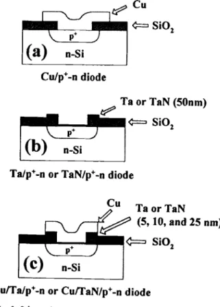
TheCu/Ta/pt-n and Cu/TaN/p°-n junction diodes were fabricated for the study of Ta and TaN barrier capability. The starting materials were 4-in., (100)-oriented, n-type silicon wafers with 4-7 11 cm nominal resistivity. After
RCA standard cleaning, the wafers were thermally
oxi-dized at 1050°C in steam atmosphere to grow a 500 nm oxide layer. Diffusion regions with areas 500 >< 500 and 1000 X 1000 p.m2 were defined on the oxide-covered wafers using the conventional photolithographic
tech-nique. The p-n junctions with junction depths of 0.3 p.m
were formed by BF implantation at 40 keV to a dose of
3 x 10° cm' followed by furnace annealing at 900°C for 30 mm in N, ambient.
After the junctions were formed, the wafers were pre-pared for Ta or TaN barrier layer deposition. In this study, a dc magnetron sputtering system with a base pressure of 1—2 X
i0°
Torr and with no intentional substrate heating and bias was used. The Ta films were sputtered using a Ta target in Ar ambient at a pressure of 7.6 mTorr, while theTaN films were reactively sputtered using the same Ta target in an Ar/N2 gas mixture at the same pressure of 7.6 mTorr.
The flow rates of Ar and N, into the sputtering chamber
were 24 and 6 sccm, respectively, for making the Ar/N2 gas
mixture.'8 Prior to each sputter deposition, the target was
cleaned by presputtering with the shutter closed for 10 mm. The Ta and TaN films were deposited at a sputtering
power of 200 W to a thickness of 25, 10, and 5 nm
sepa-rately The deposition rates of Ta and TaN films were
determined to be 2.94 and 2.07 nm/mm, respectively After the barrier layer deposition, Cu films of 200 nm thickness were deposited on the barrier metal using the same
sput-tering system without breaking the vacuum. Finally Cu
patterns were defined and etched using dilute (5 vol %) HNO,, while Ta and Ta nitrides were etched using SF,/N, plasma for the preparation of Cu/Ta/pt-n and Cu/TaN/pt-n diodes. For comparisoCu/TaN/pt-n, the thermal stability of Cu/pt-Cu/TaN/pt-n
diodes without a barrier layer as well as Ta/p-n and
TaN/ptn diodes without a Cu overlayer was also investi-2538 J Electrochem. Soc., Vol. 145, No. 7, July 1998 The Electrochemical Society, Inc.
J. Electrochem. Soc., Vol. 145, No. 7, July 1998 The Electrochemical Society, Inc. 2539 gated. The schematic cross sections of these differently
metallized p-n junction diodes are illustrated in Fig. 1. To investigate thermal stability of the Cu/Ta/p°-n and Cu/TaN/pt-n diodes, the diodes were thermally annealed at
various temperatures ranging from 200 to 800°C for 30 mm
in N2 ambient. Leakage current was measured at a reverse
bias of —5 V using an HP-4145B semiconductor parameter analyzer; the measured diodes have an active area of 500 X 500or 1000 X 1000 urn, and at least 30 diodes were meas-ured in each case. For material analysis, unpatterned
sam-ples of barrier/Si, Cu/barrier/Si, and Cu/barrier/Si02/Si structures were also prepared. These samples were processed
in the same process run with the patterned samples of
junc-tion diodes except a number of thicker Ta and TaN samples of Ta/Si and TaN/Si specialized for X-ray diffraction (XRD)
analysis. Sheet resistance of the multilayer structures was measured using a four-point probe. XRD analysis using a 30 keV copper Ka radiation was used for phase identifica-tion. Scanning electron microscopy (SEM) was employed to observe surface morphology and microstructure.
Resultsand Discussion
Electricalmeasurements—Barrier capability of thin Ta and TaN films was investigated by evaluating the thermal stability of Cu/Ta/pt-n and Cu/TaN/pt.n junction diodes using electrical measurements. We analyzed the
distribu-tions of leakage current density for the annealed diodes
and related the results of electrical measurements to other results obtained by sheet resistance measurement, XRD
analysis, and SEM observation.
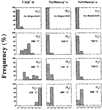
Cu/Ta/p -n junction diodes.—Figure 2 illustrates the sta-tistical distributions of reverse bias leakage current
densi-ty measured at —5 V for the Cu/Ta(25 nm)/p-n, Cu/Ta
(10 nm)p-n, and Cu/Ta(5 nm)/p*n junction diodes
annealed at various temperatures. The Cu/Ta(25 nm)/p-n diodes remained stable after annealing at temperatures up to 550°C but suffered moderate degradation in electrical
characteristic at 600°C; annealing at 650°C resulted in
severe degradation (Fig. 2a). For the Cu/Ta(10 nm)/p-n diodes, the diodes remained stable after annealing at
tern-(b)
n-SipJ
1
(c)
n-SiCuITa/p1.n or Cu/TaN/p4-n diode
Fig. 1. Schematic cross sections of (a) Cu/pFn, (b) barrier/p--n, and (c) Cu/barrier/p.n junction diodes.
Fig. 2. Histograms showing the distributions of reverse bias leakage current density for (a) Cu/Ta(25 nm)/p-n, (b) Cu/Ta (10 nm)/p-n, and (c) Cu/To(5 nm)/p-n junction diodes annealed at various temperatures.
peratures up to 500°C, while a number of diodes suffered moderate degradation after annealing at 550°C; however, about 50% of the diodes survived even after annealing at 600°C (Fig. 2b). As for the Cu/Ta(5 nm)/p-n diodes, they
started to show degradation after annealing at 500°C
(Fig. 2c). This indicates that thermal stability of the
Cu/Ta/pt-n junction diodes may be severely degraded by reducing the Ta barrier layer thickness below 5 nm. Cu/TaN/pp-n junction diodes—The barrier properties of
Ta can be significantly improved by adding impurities, such as N and 0, to the Ta film.'819 If solubility limit of the impurity is exceeded, solute atoms in the Ta grain are
expected to be segregated to the grain boundaries, result-ing in obstruction of the fast paths for copper diffusion. It
was reported that the grain size and atomic density of
reactively sputtering deposited Ta-N films, respectively, decreased and increased as the nitrogen concentration in
the Ta—N films was increased; moreover, the bcc-Ta, Ta2N, TaN, and Ta,N6 phase appeared in succession with the increase of the nitrogen content.18 In addition, TaN is chemically inert to Si and Cu, and it has been reported that the contact system of Cu/TaN/Si is thermally very
stable.23 The superiority of TaN films in thermal stability
over the pure Ta film was also reported.2°
Figure 3 shows the statistical distributions of reverse
bias leakage current density for the Cu/TaN/p-n junction diodes of different TaN barrier thickness annealed at var-ious temperatures. For the diodes with a 25 nm thick TaN barrier, the devices remained stable after annealing at tem-peratures up to 700°C. After annealing at 750°C, though many devices failed, more than half of the tested diodes still survived (Fig. 3a). This feature of failure is probably related to the Cu diffusion through localized defects in the
annealed TaN layer. For the diodes with a 10 nm thick TaN
barrier, the devices suffered moderate degradation after annealing at 650°C and degraded severely after annealing at 700°C (Fig. 3b). For the Cu/TaN(5 nm)/p-n diodes, the
5 nm TaN film was proved to be an effective barrier
against Cu diffusion at temperatures up to 500°C. As the
annealing temperature was raised to 550°C, the diodes
started to show degradation (Fig. 3c). Comparative results CuIFa(25nm)/p-u CuITa(lOnm)1p-n Cu/Ta(Snm)/p'-Ii
10i
I
,
,
.T L
10 10l0'l0 I0 1010' 10 I0 I0'IO'lO' 10 10' l0'LO10'l0 I0'lO 0'
Leakage Current Density (A/cm2)
Cu/p'-n diode
Cu
Si02
Ta or TaN (5Onm)
:
Si02Ta/p*_n or TaN/p'-n diode
Cu Ta
or TaN
(5, 10, and 25 nm)
100' r—___'____'___'
'1
(a,) (ba)60 700 C 650 C 550C
40
20
Leakage Current Density (A/cm2)
Fig. 3. Histograms showing the distributions of reverse bias leakage current density for (a) Cu/TaN(25 nm)/p-n, (b) Cu/TaN
(10 nm)/p-n, and (c) Cu/TaN(5 nm)/p-n junction diodes
annealed at various temperatures.
ofbarrier effectiveness for Ta and TaN films of different thickness are summarized in Table I. The results show that
the barrier capability of a Ta layer can be substantially improved by incorporation of nitrogen using reactive
nitridation technique. Moreover, thermal stability of the
Cu/Ta/pt-n and Cu/TaN/p-n diodes was found to be
dependent on the thickness of the barrier, implying that Cu diffusion in the barrier layer is mainly controlled by film defects, such as grain boundaries, voids, and dislocations.
Cu/p-n, Ta/p n and TaN/p-n junction diodes—For
comparison, the Cu/p-n diodes without a barrier layer and the barrier/p-n diodes without a Cu overlayer werealso fabricated for thermal stability study. Figure 4
illus-trates the distributions of reverse bias leakage current density for the Cu/p-n, Ta/p-n, and TaN/p4-n junction diodes annealed at various temperatures. The Cu/pt-n diodes suffered severe degradation after annealing at 200°C
(Fig. 4a), while the Ta/pt-n and ThN/p-n diodes were able
to retain their integrity up to at least 800°C. Thus, the
degradation of Cu/Th/p-n and Cu/TaN/pt-n diodes (Fig. 2 and 3) was attributed to the presence of Cu overlayer.
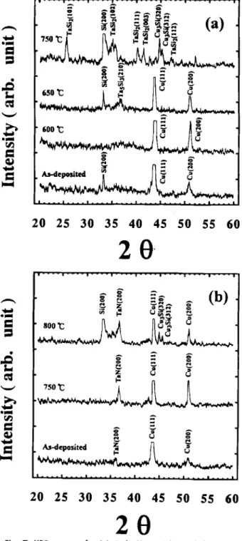
Material Analyses.—XRD analysis—The
crystallograph-ic structure of sputter-deposited TaNs depends on the con-centration of nitrogen in the TaNs film.u Figure 5 shows the XRD spectra for the Ta(300 nm)/Si sample annealed at various temperatures. Diffraction patterns taken from the as-deposited Ta layer was indexed to be —Ta.29 For the
sample annealed at 650°C, the spectrum remained
unchanged as compared with the as-deposited sample. However, a number of weak TaSi2 30 peaks appeared for theTableI. Comparative results of barrier effectiveness for Ta and
TaN films evaluated by electrical measurement on the
Cu/barrier/p-n junction diodes.
Ta______ TaN Barrier layer 25 nm 10 nm 5 nm 25 nm 10 nm 5 nm Thermal stability 550°C 500°C 450°C 700°C 600°C 500°C temperature 100 (a0)
'ELT L L . 7O0cj
[
s00'
(t) 00't0't0'00'l0'F0l0' 1O'101O'10°F0'i0F0' 10'0010 'lO'FO'FO"FQ'Leakage
Current Density (A/cm2)
Fig. 4. Histograms showing the distributions of reverse bias
leak-age current density for (a) Cu/pt-n, (b) Ta(50 nm)/p4'-n, and (c)
TaN(50 nm)/p-n junction diodes annealed at various temperatures.
sampleannealed at 700°C. After annealing at 800°C, signals representing the crystalline phase of TaSi2 became much stronger, indicating significant grain growth. Since Ta
sili-cidation was not observed at 600°C and the electrical
char-acteristics of Cu/Ta/pt-n diodes failed at temperatures below 600°C (Fig. 2), we excluded the possibility of Ta sili—
cidation to be one of the Ta-barrier failure mechanisms for the Cu/Ta/p*_n junction diodes. Noya et al. reported that Ta3Si3 or amorphous layer formation at the Ta/Si interface
preceded the TaSi2 growth.30'32 However, our results of XRD
analyses showed only TaSi2 phase in the thermally annealed
CaTaN(25nm)/p-oo Cu/TaN(IOnrn)/p.n Cu/TaN(Snm)/p.n CuIp°-n Ta(5Onm)/p.n TaN(50mu)/p'.n
I
10'l0'l0'F0I0'10'10' 10'lO'IO 'F0F0'l0I0' 00'IO'IO'IOIO' 00F0'
I
20 25 30 35 40 45 50 55 60
20
Fig. 5. XRD spectra for Ta(300 nm)/Si sample annealed at
J. Electrocl-iem. Soc., Vol. 145, No. 7, July 1998 The Electrochemical Society, Inc. 2541 Ta/Sisystem, similar to the results reported by Holloway et
—
-al.2° This discrepancy might result from the difference in
deposition temperature as well as thickness of Ta metal and annealing conditions between Noya's and ours.
Figure 6 shows XRD spectra for the TaN(300 nm)/Si
sample. The diffraction patterns taken from the
as-deposited TaN layer was indexed to be cubic TaN.33 The spectrum remained unchanged even after the sample was
annealed at 800°C, indicating structural integrity of the TaN(300 nm)/Si sample. By comparing the XRD spectra of the TaN/Si samples (Fig. 6) with those of the Ta/Si samples (Fig. 5), we found clearly that the contact system of TaN/Si
is chemically more stable than that of Ta/Si.
Figure 7 shows XRD spectra for the Cu/Ta(25 nm)/Si and Cu/TaN(25 nm)/Si samples after annealing at various temperatures. For the Cu/Ta/Si sample annealed at 650°C, signal of Ta5Si3 phase34 was detected; after annealing at
750°C, signal of Cu35 disappeared while many peaks
relat-ing to Ta silicide and Cu suicide36 appeared, indicatrelat-ing
complete failure of the Ta-barrier film (Fig. 7a). Compared
___________________________________________
with the XRD spectra for the Ta/Si samples (Fig. 5), we found that the presence of Cu film on the surface of the Ta/Si structure accelerated the formation of Ta silicide.2° Suicide signals did not appear for the Cu/TaN/Si sample
thermally annealed at temperatures up to 750°C (Fig. 7b).
2
Clearly,thermal stability of the Cu/TaN/Si structure is
supe-rior to that of the Cu/Ta/Si contact system. Furthermore, raising the annealing temperature to 800°C resulted in the appearance of Cu silicide signal, but the Ta suicide signal
was not detected (Fig. 7b). These results imply that the
failure of Cu/TaN/p-n diodes at 750°C or below (Fig. 3) was not related to Ta silicidation at the TaN/Si interface. Instead, Cu atoms diffused through the annealed TaN film
via local defects (such as grain boundaries, voids, and
stress-induced weak points) should be blamed.
Sheet resistance measurement—The sheet resistance
change of annealed samples, normalized to the
as-deposit-ed sheet resistance value, is denotas-deposit-ed as Rs/Rs% and
defined as follows
= Rsc,.rneaI RS._dePOtd x100 %
Rs
Figure 8 shows the percentage change of sheet resistance
vs. annealing temperature for the samples of Cu/Ta
20 25
3035 40 45 50 55
60
20
Fig. 7. XRD spectra for (a) Cu/1at25 nm)/Si and (b) Cu/TaN (25 nm)/Si samples annealed at various temperatures.
--4-- Cu,Ta/Si —--- CufFaN/Si
*
—e—Cufra/SiOJSi/
'I —R--CUIFaN/SiOJSiAs-deposited
0I
25 400
500 600 700 800
2
0
Temperature
(°C)
Fig.8. Percentage change of sheet resistance vs. annealing
tern-Fig. 6. XRD spectra for TaN(300 nm)/Si sample annealed at var- perature for the samples of Cu/Ta(25 nm)/Si, Cu/TaN(25 nmj/Si
ious temperatures. Cu/Ta(25 nm)/Si02/Si, and Cu/TaN(25 nm)/Si02/Si.
i
J4L
20
25
30
35 40 45 50 55 60
\1
Cz
800 tz
I
s-eposite 700 t6000
4000
2000
20 25 30
35 40 45
50 55 60
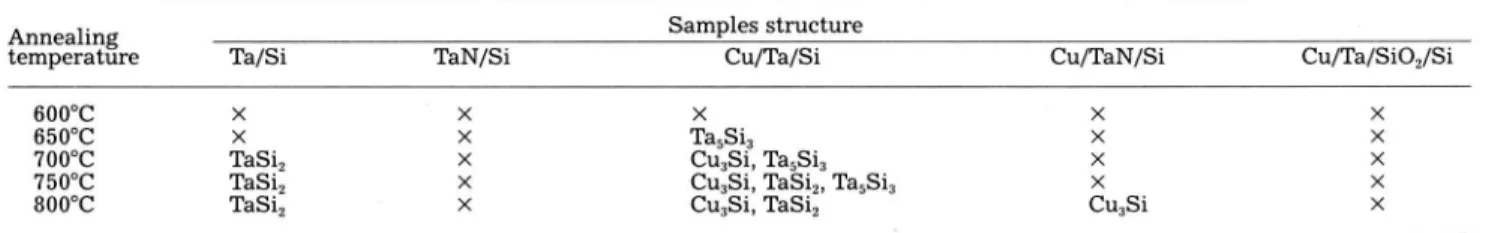
Table II. Compound phases detected by XRD analysis for various multilayer structures studied in this work.°
Annealing
temperature
Samples structure
Ta/Si TaN/Si Cu/Ta/Si Cu/TaN/Si Cu/Ta/5i02/Si
600°C x x x
x
X 650°C 700°C X Th5i2 XX Ta55i3Cu3Si, Ta5Si3
x X
)<
x
750°C TaSi2 X Cu3Si, TaSi2, Ta55i3
x
x800°C TaSi2 X Cu3Si, TaSi3 Cu3Si X
a indicates
no observation of compound phase (except TaN).
(25 nm)/Si, Cu/TaN(25 nm)/Si, Cu/Ta(25 nm)/Si02/Si, and Cu/TaN(25 nm)/Si02/Si. For the Cu/Ta(25 nm)/Si sample,
the sheet resistance remained constant after annealing at
temperatures up to 700°C, but a dramatic increase occurred
-.40311 P0.14kV x4.Bek4H;1.
20:0kv X4.Oék
Fig. 9. Top view and oblique view SEM micrographs for the Cu/TaN(25 nm)/p-n diodes annealed at (a) and (b) 700°C, and (c), (d), (e), and (f) 750°C. The micrographs (c) and (d) were taken on a slightly degraded diode, and (e) and (f) were taken on a severely degraded diode.
J. Electrochem. Soc., Vol. 145, No. 7, July 1998 The Electrochemical Society, Inc. 2543
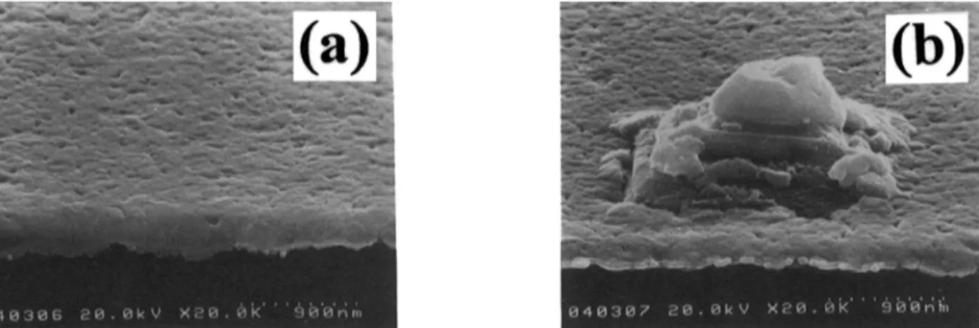
Fig. 10. SEM micrographs for the Cu/Ta(25 nm)/p..n diodes annealed at (a) 600 and (b) 650°C.
after annealing at 750°C. Sheet resistance for the Cu!
TaN(25 nm)/Si sample remained unchanged after
anneal-ing at temperatures up to 750°C but made a significant increase after annealing at 800°C. The increase in sheet
resistance for the Cu/Ta(25 nm)/Si and Cu/TaN(25 nm)/Si samples reflects the consumption of conductive Cu layer due to Cu3Si formation, as confirmed by the XRD analysis shown in Fig. 7. Although sheet resistance of the Cu/Ta (25 nm)/Si sample remained unchanged after annealing at 700°C, the results of electrical measurement showed that
the Cu/Ta(25 nm)/p*_n junction diodes suffered severe
degradation after the devices were annealed at 650°C. This
indicates that electrical measurement is a much more sen-sitive technique for barrier failure detection.
For the samples with a 500 nm oxide layer between the
barrier metal and Si substrate, sheet resistance of the
Cu/Ta(25 nm)/Si02/Si and Cu/TaN(25 nm)/Si02/Si sam-ples remained constant up to at least 800°C. Moreover, no
signal relating to Ta—Si or Cu—Si compound was detected
by XRD analysis. The different results between the
Cu/barrier/Si02/Si and Cu/barrier/Si samples imply that the Si substrate in the Cu/barrier/Si contact system acted as a Cu-sink, which plays an important role in
determin-ing the thermal stability of the Cu/barrier/Si structure.
Fig. 11. SEM micrographs for the Cu/TaN(5 nm)/p-n diodes annealed at (a) and (b) 550°C, and (c) 600°C. The micrograph (a) was taken on a diode of low leakage current while (b) was taken on a severely degraded diode.
44
Fig. 12. SEM micro9raphs for the Cu/Ta(5 nm)/p-n diodes annealed at (a) 500 and (b) 550°C. Comparative results of thermal stability for the
multilay-er structures studied in this work based on XRD analysis are summarized in Table II.
SEM observation.—SEM was used to investigate the
sur-face and cross-sectional morphology of the thermally
annealed Cu/barrier/p*_n junction diodes. Figure 9 shows the surface morphology of Cu/TaN(25 nm)/p-n junction diodes annealed at 700 and 750°C. Surface morphology
of the diodes remained stable after annealing at 700°C (Fig. 9a and b). After annealing at 750°C, some of the
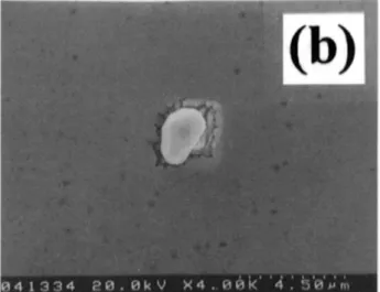
diodes degraded severely (with high leakage current) while the others were only slightly degraded with reverse bias leakage current density less than 100 nA/cm2, as shown in Fig. 3. For those diodes showing only a slight degradation, surface morphology of the diodes is shown in Fig. 9c and d; only a number of small openings were observed on the surface. For those severely degraded diodes, Fig. 9e and f
shows that there are highly localized protrusions on the
diode's surface. Thus, failure of the devices is associated with these protrusions, which were presumably caused by Cu diffusion through the localized weak points in the TaN barrier layer. For the Cu/Ta(25 nm)/p-n junction diodes, SEM micrographs revealed that the device's structure was able to remain stable after annealing at 600°C, as shown in Fig. ba; however, localized protrusions were found after annealing at 650°C, as shown in Fig. lOb.
Figure 11 shows the SEM micrographs for the Cu/TaN
(5 nm)/p-n diodes annealed at 550 and 600°C. After
annealing at 550°C, the diodes with a low leakage current density nearly retained their structural integrity (Fig. ha), while a few highly localized protrusions were found for the diodes with a large leakage current density (Fig. hlb). After annealing at 600°C, dense localized protrusions were
found on the surface of the annealed samples (Fig. lic).
For the Cu/Ta(5 nm)/p-n diodes, SEM observation
revealed that the device's structure basically remained sta-ble after annealing at 500°C (Fig. 12a). However, Cu
pene-trated the Ta barrier to form 1"-Cu3Si precipitate after annealing at 550°C. This precipitate extends into the Si
sub-strate and out of the sample surface, as shown in Fig. 12b. Based on the results of SEM observation (Fig. 9, 10, 11, and 12) and electrical measurement (Fig. 2 and 3), we
con-clude that the electrical degradation for the thermally
annealed Cu/barrier/p-n junction diodes is closely relat-ed to the presence of highly localizrelat-ed defects in the barri-er laybarri-ers. This suggests that the failure of vbarri-ery thin Ta and TaN barrier is principally due to permeation of Cu atoms through the barrier layer via local weak points (including grain boundaries) during the process of thermal annealing.
Conclusion
Thermalstability of very thin sputtered Ta and reactive-ly sputtered TaN films used as a diffusion barrier between Cu and silicon substrate was investigated. We found that thermal stability of the Cu/barrier/Si system depends on
the barrier thickness and that the presence of Cu film on the Ta and TaN barrier surface of the barrier/Si structure
accelerated the formation of Ta silicide. The Cu/Ta/p-n
junction diodes with a 25 nm thick Ta barrier were able to sustain a 30 mm thermal annealing at temperatures up to 550°C without causing degradation to the device's electri-cal characteristics. For a 5 nm thick Ta barrier layer, ther-mal stability of the Cu/Ta/Si diodes was reduced to 450°C.
The barrier capability of the sputtered Ta layer can be effec-tively improved by incorporation of nitrogen in the Ta layer
using reactive sputtering technique. The Cu/TaN/p-n junc-tion diodes with a 25 nm thick TaN barrier remained ble up to 700°C. For a 5 nm thick TaN layer; thermal sta-bility of the Cu/TaN/pt-n diodes was reduced to 500°C. The failure of very thin Ta and TaN barrier was not relat-ed to Ta silicidation at the barrier/Si interface; instead, Cu atoms diffused through the barrier layer during the process
of thermal annealing via local defects, such as grain
bound-aries and stress-induced weak points, leading to failure of the barrier layer.
Acknowledgments
Thiswork was supported by the National Science Council (ROC) under contract no. NSC86-2215-E-009-040.
Manuscript received April 7, 1998.
The National Chiao-Tung University assisted in meeting the publication costs of this article.
REFERENCES
1. R. J. Gutmann, T. P. Chow, A. E. Kaloyeros, W. A.
Lan-ford, and S. P. Murarka, Thin Solid Films, 262, 177
(1995).
2. N. Awaya, H. Inokawa, E. Yamamoto, Y. Okazaki, M.
Miyake, Y. Arita, and T. Kobayashi, IEEE Trans. Electron Devices, ED-43, 1206 (1996).
3. V. M. Dubin and Y. S. Diiamand, J. Elect rochem. Soc.,
144, 898 (1997).
4. J. C. Chiou, K. C. Juang, and M. C. Chen, J. Elec-trochem. Soc., 140, 177 (1995).
5. J. C. Chiou, Y. J. Chen, and M. C. Chen, J. Electron.
Mater., 23, 383 (1994).
6. C. A. Chang, J. Appl. Phys., 67, 566 (1990).
7. S. H. Corn and J. L. Falconer, J. Vac. Sci. Technol., A6,
1012 (1988).
8. Y. Shacham-Diamand, A. Dedhia, D. Hoffstetter, and
W. G. Oldham, J. Elect rochem. Soc., 140, 2427 (1993).
9. A. L. S. Loke, C. Ryu, C. P. Yue, J. S. H. Cho, and S. S. Wong, IEEE Electron Device Lett., EDL-17, 549
(1996).
10. J. C. Chiou, H. I. Wang, and M. C. Chen, J. Elect rochem. Soc., 143, 990 (1996).
11. M.-A. Nicolet, Thin Solid Films, 54, 415 (1978). 12. M. Wittmer, J. Vac. Sci. Technol., A2, 273 (1984).
13. H. Ono, T. Nakano, and T. Ohta, Appl. Phys. Lett., 64,
1511 (1994).
14. W. K. Yeh, T. T. Wu, M. H. Tsai, S. C. Sun, J. C. Chuang,
and M. C. Chen, VMIC Proc., June 1996, p. 541. 15. S. D. Kim, S. G. Jin, M. R. Hong, and C. T. Kim, J.
Elec-J. Electrochem. Soc., Vol. 145, No. 7, July 1998 The Electrochemical Society, Inc. 2545
trochem. Soc., 144, 664 (1997).
16. S. Q. Wang, J. Appl. Phys., 73, 2301 (1993).
17. J. C. Chiou, K. C. Juang, and M. C. Chen, J. Elec-trochern.Soc., 142,2326 (1995).
18. X. Sun, E. Kolawa, J. S. Chen, J. S. Reid, and M. A.
Nicolet, Thin. Solid Films, 236, 347 (1993).
19. K. Holloway and P. M. Fryer, Appl. Phys. Lett., 57,
1736 (1990).
20. K. Holloway, P M. Fryer, C. Cabral, Jr., J. M. E.
Harp-er, P J. Bailey, and K. H. KellehHarp-er, J. Appi. Phys., 71,
5433 (1992).
21. E. Kolawa, J. S. Chen, J. S. Reid, P J. Pokela, and M. A. Nicolet, J. Appi. Phys., 70, 1369 (1991).
22. T. Oku, E. Kawakami, M. Uekubo, K.Takahiro, S.
Yam-aguchi, and M. Murakami, Appl. Surf. Sci., 99, 265
(1996).
23. M. Takeyama, A. Noya, T. Sase, and A. Ohta, J. Vac.
Sci.Technol.,B14,674(1996).
24. R. G. Schad, F. Cardone, and L. Stolt, J. Appi.
Phys., 73, 301 (1993).
25. M. S. Angyal, Y. S. Diamand, J. S. Reid, and M. A.
Nicolet, Appi. Phys. Lett., 67, 2152 (1995).
26. T. Vasilos and W. Kingery, J. Ceram. Soc., 37, 409
(1954).
27. B. S. Kang, S. M. Lee, J. S. Kwak, D. S. Yoon, and K.
Baik, J. Electrochem. Soc., 144, 1807 (1997).
28. T. T. Wu, Masters Thesis, National Chiao-Tung Univer-sity, Taiwan (1996).
29. JCPDS Files card no. 25-1280. 30. JCPDS Files card no. 38-0483.
31. A. Noya, M. Takeyama, K. Sasaki, and T. Nakanishi, J. Appl. Phys., 76, 3893 (1994).
32. A. Noya, M. Takeyama, K. Sasaki, E. Aoyagi, and K.
Hiraga, J. Vac. Sci. Technol., A15, 263 (1997). 33. JCPDS Files card no. 32-1283.
34. JCPDS Files card no. 6-0594. 35. JCPDS Files card no. 4-0836. 36. JCPDS Files card no. 23-224.
Investigation of Boron Penetration Through Thin Gate
Dielectrics Including Role of Nitrogen and Fluorine
Mifra Navi* and Scott1. Dunham**
Departmentof Electrical and Computer Engineering, Boston University, Boston, Massachusetts 02215, USA
ABSTRACT
This work examines boron penetration from p polysilicon through 50—70 A gate dielectrics following B or BF2
implantation. Gate oxides were grown in N20/02 mixtures with average nitrogen contents varying from 0 to 1.4%. A series
of capacitance—voltage measurements were used to determine the amount of boron penetration, and secondary ion mass spectroscopy measurements were carried out to measure the depth profiles of incorporated nitrogen and fluorine. In addi-tion, to better understand the role of fluorine, experiments were carried out to investigate the redistribution of fluorine in the poly/Si02/Si system.
Introduction
Scalingof complementary metal-oxide semiconductor
(CMOS) processes down to submicron channel lengths
greatly improves device density and circuit speed but
in-troduces many challenges in process technology. One
diffi-culty is the scaling of the gate dielectric, particularly for
the fabrication of p polysilicon gates in p-channel
de-vices. The concern is the diffusion of boron through the
gate oxide. Boron penetration from the p-polysilicon gates can cause fluctuations in flatband voltage (VFB)' which are accompanied by increases in electron charge
trapping and inverse subthreshold slope.2
The diffusivity of boron can be modified by many fac-tors. Increased boron diffusivity is observed when fluorine or hydrogen is introduced in the oxide.3 In contrast, incor-poration of nitrogen in Si02 is known4'5 to reduce boron diffusivity. Injection of silicon interstitials in the oxide has also been suggested to decrease boron diffusivity6
It has been proposed that boron diffusion increases with decreasing oxide thickness.7 However, recent work has found no thickness dependence.3'8'5 Aoyama et al.,3 who have carried out perhaps the most extensive set of experi-ments on boron penetration in thin oxides, found no oxide thickness dependence on boron diffusion in the absence of
fluorine. However, in the presence of fluorine, they
ex-tracted higher B diffusion for thinner oxides. The
differ-ence was attributed to the fact that the boron diffusion
strongly depends on fluorine content of the oxide, which was presumed to vary with thickness.
Although B diffusion is expected to depend locally on the oxide structure and composition, modeling to date has been
generally limited to determining an effective average
dif-*Electrochemical
Society Student Member.
*ElectrochemicalSociety Active Member.
fusivity as a function of processing conditions.5'7 To gen-erate a predictive model, it is important to consider the un-derlying oxide composition and structure that results in the observed diffusivity. In order to help address these issues, we have conducted a series of experiments in which both boron diffusivity as well as the composition of the oxide were studied.
Experimental
MOS capacitors were fabricated on 4 in. silicon (100)
wafers with background phosphorus doping of 2—4 (1 cm. A field oxide of 0.6 m was grown and etched to define
active areas (100 )< 100 p.m). Gate dielectrics were grown in pure 02 at 870°C, pure N20 at 910°C, or an NZO/02 at
870°C mixture. Undoped polysilicon was deposited at
625°C immediately following gate dielectric growth. The polysilicon was implanted to a dose of 5 x i0 cm2, using at 40 keV and BF or B* at 25 keV. A low-temperature cap oxide of 0.5 m was deposited at 425°C to avoid out-diffusion of boron. Wafers were annealed at 900—1050°C
for various times to ensure boron penetration. After
removal of the cap oxide, the polysilicon was patternedand etched. Aluminum deposition followed by sintering was performed on some samples and capacitance—voltage measurements showed no difference between capacitors with and those without aluminum electrodes.
Capacitors were characterized using high-frequency (100 kHz) capacitance—voltage (Cv) measurements. In
ad-dition, secondary ion mass spectroscopy (SIMS) measure-ments were carried out° to quantify the amount of nitrogen and fluorine incorporation in the gate oxides, as well as in the polysilicon and substrate.