自我補償之固定長度乘法器及其應用
66
0
0
全文
(2) 自我補償之固定長度乘法器及其應用 Design of Self-Compensation Fixed-Width Multiplier and Its Applications 學生:黃弘安. Student : Hong-An Huang. 指導教授:張錫嘉. Advisor : Hsie-Chia Chang. 國立交通大學 電子工程學系 電子研究所碩士班 碩士論文. A Thesis Submitted to Department of Electronics College of Electrical Engineering and Computer Science National Chiao Tung University In Partial Fulfillment of the Requirements For the Degree of Master In Electronics Engineering. October 2005 Hsinchu, Taiwan, R.O.C..
(3) 自我補償之固定長度乘法器及其應用 學生 : 黃弘安 指導教授 : 張錫嘉 國立交通大學 電子工程學系 電子研究所碩士班. 摘. 要. 在本論文中,我們提出一個利用自我補償方法的固定長度乘法器架構。 在這個架構中,藉由進位估算方程式,只需要少量的全加器就能夠計算所 需要的進位補償值。為了減少因為刪除運算元件所造成的誤差,我們的架 構會根據不同的乘法器長度而有其相對應的進位估算方程式,以達到最佳 的效果。經由模擬結果發現,使用所提出的乘法器架構,刪除誤差可以降 低到只有 Direct-truncated 乘法器的 15%,在面積部份,則是縮小到只有傳 統 Booth 乘法器的 60%。此外,我們也將這個乘法器架構應用在 128 點 FFT 中,和使用 Direct-truncated 乘法器的 128 點 FFT 架構相比,我們的 SQNR (Signal to Quantization Noise Ratio)高出了 10dB,而面積只增加了 2%左右; 相較於傳統的 Booth 乘法器架構,我們可以降低 10%的面積,而且只減少 約 1dB 的 SQNR。 ii.
(4) Design of Self-Compensation Fixed-Width Multiplier and Its Applications Student: Hong-An Huang Advisor: Hsie-Chia Chang Institute of Electronics National Chiao Tung University. ABSTRACT. This thesis introduces a self-compensation method for fixed-width multiplier which receives two n-bit inputs and produces an n-bit product. The truncated part that produces the carry-out bit is replaced with carry-estimation equations. In order to reduce the truncation errors, different input-width multipliers will correspond to different carry-estimation equations. Simulation results show that our self-compensation method can lead to 85% reduction of truncation errors while compared with direct-truncated multipliers, as well as 40% reduction in area of a multiplier while compared with traditional Booth multipliers. In contrast with the 128-FFT using direct-truncated multipliers, our 128-FFT approach has 10dB SQNR improvement and only 2% circuit penalty.. iii.
(5) 誌. 謝. 一轉眼,二年的研究所生活就過去,在這兩年中學到許多作學問的方法以及一些處世 的道理。 其中要感謝的人非常多,首先最要感謝的當然是我的指導教授張錫嘉博士。 這兩年老師不但在研究上給予我許多的指導和方向,讓我能有一些研究成果,在生活 上,老師也是一位很好的諮商顧問,當我們在生活上糟遇到問題,都會耐心的聽我們訴 說,並且給我們適當的建議。 再來要感謝的就是林建青學長,每當我遇到問題時,學 長總是不厭其煩的幫我解答,讓我在研究的路上,能更加的順暢。此外,也要感謝 oasis 的同學和學弟們,這兩年來,因為有你們的陪伴,讓我的生活更加充實、快樂,真的很 高興能認識你們這群好伙伴。最後,再一次的感謝在這兩年中,曾經幫助過我的每一位。. iv.
(6) CONTENTS 中文摘要………………………………………………………………………………………ii 英文摘要……………………………………………………………………...………………iii 誌謝……………………………………………………………………...………………iv 目錄……………………………………………………………………………...…………….v 圖目錄……………………………………………………………………………..…………vii 表目錄…………………………………………………………………………...…………ix Chapter 1 Introduction........................................................................................................... - 1 1.1 Motivation ....................................................................................................... - 1 1.2 Thesis Organization ......................................................................................... - 2 Chapter2 Existed Fixed-Width Multipliers ........................................................................... - 3 2.1 S-J Jou Approach ............................................................................................. - 4 2.2 K-J Cho Approach ........................................................................................... - 7 2.3 L-D Van Approach......................................................................................... - 15 Chapter3 Proposed Self-Compensation Multiplier.............................................................. - 21 3.1 Calculation of Error-compensation bias ........................................................ - 21 3.2 Proposed Structure......................................................................................... - 28 3.3 Performance Analysis .................................................................................... - 31 Chapter4 Application of Fixed-Width Multipliers in FFT .................................................. - 34 4.1 Introduction to 128-Point FFT....................................................................... - 34 4.2 128-Point FFT Architecture........................................................................... - 38 4.2.1 Module 1............................................................................................. - 39 4.2.2 Module 2............................................................................................. - 40 4.2.3 Module 3............................................................................................. - 41 v.
(7) 4.3 Simulation Results......................................................................................... - 42 Chapter5 Implementation Results for 128-point FFT ......................................................... - 44 5.1 Approach 1..................................................................................................... - 44 5.2 Approach 2..................................................................................................... - 46 5.3 Comparison.................................................................................................... - 51 Chapter6 Conclusion ........................................................................................................... - 52 BIBLIOGRAPHY ............................................................................................................... - 53 -. vi.
(8) List of Figures FIG 1-1: 8-BIT BOOTH MULTIPLIER...........................................................................................- 1 FIG 2-1: PARTIAL PRODUCT OF 8-BIT BOOTH MULTIPLIER ........................................................- 3 FIG 2-2: EXAMPLE OF 6 X 8 BOOTH MULTIPLIERS ....................................................................- 4 FIG 2-3: 6 X 8 FIXED-WIDTH MULTIPLIER WITH S-J JOU APPROACH ..........................................- 6 FIG 2-4: STRUCTURE OF K-J CHO SCHEME...............................................................................- 8 FIG 2-5: PARTIAL PRODUCTS FOR Y3”Y2”Y1”Y0” = 0001 .........................................................- 10 FIG 2-6: KARNAUGH MAP REPRESENTATION FOR (A)LP_CARRY_0 AND (B)LP_CARRY_1 FOR N = 10 ..................................................................................................................................- 12 FIG 2-7: CIRCUIT OF APPROXIMATE CARRY FOR N = 10...........................................................- 12 FIG 2-8: APPROXIMATE CARRY GENERATION CIRCUITS (A)N = 10 (B)N = 14...........................- 14 FIG 2-9: FIXED-WIDTH MULTIPLIER WITH K-J CHO APPROACH FOR N = 8...............................- 15 FIG 2-10 PARTIAL PRODUCT OF 8-BIT BAUGH-WOOLEY ARRAY MULTIPLIER .........................- 15 FIG 2-11: FIXED-WIDTH MULTIPLIER WITH L-D VAN APPROACH FOR N = 8 ...........................- 20 FIG 3-1: PARTIAL PRODUCT OF 8-BIT BOOTH MULTIPLIER ......................................................- 22 FIG 3-2: THE ERROR-COMPENSATION TABLE FOR N = 8 ..........................................................- 23 FIG 3-3: CIRCUIT OF CARRY-ESTIMATION EQUATION FOR N = 8 ..............................................- 28 FIG 3-4: CIRCUIT OF 8-BIT BOOTH MULTIPLIER WITH PROPOSED APPROACH ..........................- 29 FIG 3-5: CIRCUITS OF CARRY-ESTIMATION EQUATIONS FOR (A) N = 10 (B) N = 12 (C) N = 14 (D) N = 16 ...............................................................................................................................- 30 FIG 4-1: THE SIGNAL FLOW GRAPH OF RADIX-8 FFT ALGORITHM ..........................................- 37 FIG 4-2: THE SIGNAL FLOW GRAPH OF 128-POINT MIXED-RADIX FFT ALGORITHM ................- 38 FIG 4-3: BLOCK DIAGRAM OF 128-POINT FFT .......................................................................- 39 FIG 4-4: BLOCK DIAGRAM OF THE MODULE 1........................................................................- 40 vii.
(9) FIG 4-5: BLOCK DIAGRAM OF THE MODULE 2........................................................................- 41 FIG 4-6: BLOCK DIAGRAM OF THE MODULE 3........................................................................- 41 FIG 5-1 LAYOUT VIEW OF APPROACH 1 ..................................................................................- 45 FIG 5-2: STRUCTURE OF DDR REGISTER................................................................................- 47 FIG 5-3: OPERATIONS OF PROPOSED DDR REGISTER AT (A) CLK = 0 (B) CLK = 1.................- 48 FIG 5-4: EXAMPLE OF PROPOSED DDR REGISTER ..................................................................- 48 FIG 5-5 LAYOUT VIEW OF APPROACH 2 ..................................................................................- 50 -. viii.
(10) List of Tables TABLE 2-1: PROBABLE VALUES OF CARRYΤ-1 WITH DIFFERENT VALUES OF Β AND Τ ..................- 6 TABLE 2-2: PARTIAL PRODUCT FOR EACH ENCODED YI’ WITH N = 8 ..........................................- 7 TABLE 2-3: 8-BIT NUMBERS WITH Y3”Y2”Y1”Y0” = 1000 ..........................................................- 9 TABLE 2-4: ROUNDED VALUE OF E[Λ] FOR N = 10..................................................................- 11 TABLE 2-5: REPRESENTATION OF APPROXIMATE CARRY VALUES ............................................- 11 TABLE 3-1: THE VALUES OF Θ FOR DIFFERENT VALUES OF P3_0P2_2P1_4P0_6 ............................- 22 TABLE 3-2: THE AVERAGE CARRY FOR EACH VALUE OF Θ .......................................................- 23 TABLE 3-3: THE VALUES OF AVERAGE CARRY FOR EACH Β FOR N = 8 .....................................- 24 TABLE 3-4: THE RESULTS OF CARRY-ESTIMATION EQUATION FOR N = 8..................................- 25 TABLE 3-5: THE RESULTS OF CARRY-ESTIMATION EQUATION FOR (A) N = 10 (B) N = 12 (C) N = 14 (D) N = 16.....................................................................- 26 TABLE 3-6: THE NUMBERS OF CASES FOR EACH Β WITH N = 10 ..............................................- 27 TABLE 3-7: THE NUMBERS OF CASES FOR EACH Β WITH N = 14 ..............................................- 27 TABLE 3-8: THE NUMBERS OF CASES FOR EACH Β WITH N = 16 ..............................................- 27 TABLE 3-9: COMPARISON RESULTS OF AVERAGE ERROR .........................................................- 32 TABLE 3-10: COMPARISON RESULTS OF VARIANCE OF ERROR .................................................- 33 TABLE 3-11: COMPARISON RESULTS OF GATE COUNTS ...........................................................- 33 TABLE 4-1: SQNR OF 128-POINT FFT WITH DIFFERENT MULTIPLIER APPROACH....................- 42 TABLE 4-2: GATE COUNT OF 128-POINT FFT FOR N = 10........................................................- 43 TABLE 4-3: SQNR OF 8192-POINT FFT WITH DIFFERENT MULTIPLIER APPROACH..................- 43 TABLE 5-1: THE CHIP SUMMARY OF APPROACH 1 ARCHITECTURE...........................................- 46 TABLE 5-2: FUNCTION OF LATCH ...........................................................................................- 47 TABLE 5-3 FUNCTION OF PROPOSED DDR REGISTER .............................................................- 49 ix.
(11) TABLE 5-4: THE CHIP SUMMARY OF APPROACH 2 ARCHITECTURE...........................................- 50 TABLE 5-5: COMPARISON OF VARIOUS 128-POINT FFT ARCHITECTURES ................................- 51 -. x.
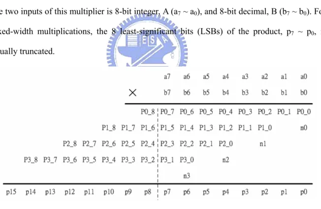
(12) Chapter 1 Introduction. 1.1 Motivation In many DSP applications, the multiplication operations have the fixed-width property. That is, the outputs and the inputs data have the same bit widths. For example, if an n-bit integer multiplicand is multiplied by an n-bit decimal, it will produce a 2n-bit product which is composed of n-bit integer and n-bit decimal. In order to reduce the hardware complexity, the n-bit decimal is usually truncated. Fig 1-1 shows the 8-bit Booth multiplier. Assume that, the two inputs of this multiplier is 8-bit integer, A (a7 ~ a0), and 8-bit decimal, B (b7 ~ b0). For fixed-width multiplications, the 8 least-significant bits (LSBs) of the product, p7 ~ p0, is usually truncated.. Fig 1-1: 8-bit Booth multiplier In order to reduce the area of multiplications, we can directly truncate the 8 least-significant columns of the partial products in Fig 1-1. By the direct-truncated method, the significant truncation errors will be introduced since the carry from the 8 least-significant columns to the 9th column is omitted. Thus, the error-compensation bias should be employed to decrease the -1-.
(13) truncation errors. In this thesis, the low-error area-efficient fixed-width multiplier based on Booth multiplier is proposed. The error-compensation bias of proposed approach is produced by the carry-estimation equations. The equations are adapted for different input width “n”. And these equations can be analyzed by few full adders. Thus, the area penalty caused by error-compensation is very small. By simulation results, the proposed fixed-width multiplier can not only reduce the truncation errors of direct-truncated multiplier but also decrease the area of standard Booth multiplier. So as to compare the performance in real applications, our fixed-width multiplier is employed in 128-point FFT architecture. Compare to the direct-truncated multiplier, the proposed multiplier has higher SQNR with only 2% increase in circuit overhead.. 1.2 Thesis Organization The organization of this thesis is described as follows. In chapter 2, three existed fixed-width multipliers are introduced. Chapter 3 shows the proposed fixed-width multiplier . The applications of proposed fixed-width multiplier are described in chapter 4. In which, the proposed multiplier is employed in 128-point FFT architecture. The design and chip implementation are shown in Chapter 5. The structure of DDR register which can reduce the operation frequency is also described in Chapter 5. Finally, Chapter 6 is the conclusion.. -2-.
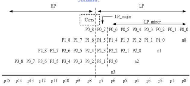
(14) Chapter2 Existed Fixed-Width Multipliers For lower computations area, the multiplications of DSP applications are usually have the fixed-width property. In other words, the bits right of decimal point are commonly omitted. Fig 2-1 shows the partial products of 8-bit Booth multiplier, it is divided into two parts, the low part (LP) and the high part (HP). The signal “Carry” means the carry from LP to HP. The adder cells required for the computation of LP in Fig 2-1 are usually truncated in DSP application. Because the carry from low part to high part was also skipped (Carry = 0), the significant truncation errors will be produced since no any error-compensation bias is employed.. Fig 2-1: Partial product of 8-bit Booth multiplier Many schemes are presented to calculate the error-compensation bias. In [1]-[3], a constant error-compensation bias is used to the retained cells. Because the bias do not adapt to the input signals, the truncation errors of these methods are large. In [4] and [5], an adaptive error-compensation bias approach which is obtained from the column of partial products adjacent to the truncated LSB is used to reduce the truncation error. In this chapter, three existed approach of fixed-width multiplier, S-J Jou approach, K-J Cho approach, and L-D Van -3-.
(15) approach, will be introduced. These schemes can not only reduce the truncation error but also decrease the area of multiplications efficiently.. 2.1 S-J Jou Approach In this section, the S-J Jou approach [6] [7] which is based on Booth multiplier will be introduced. The error-compensation bias of S-J Jou approach is generated using statistical analysis and linear regression analysis. The process of S-J Jou is represented as follows. Fig 2-2 shows the partial product of 6 x 8 Booth multiplier. The partial product is divided into two parts, the six least-significant columns are the low part (LP) and the eight most-significant columns are the high part (HP). And the signal, Carry5, means the carry from LP to HP. Now, we want to truncate the LP and to keep the HP. It will curse Carry5 equal to 0 and produce the significant truncation errors. In order to reduce the truncation errors, the error-compensation bias must be added to the HP.. Fig 2-2: Example of 6 x 8 Booth multipliers The carry from LP to HP can be obtained by Equation (2.1), where ⎣⎢ x ⎦⎥ represents the largest integer less than or equal to the number x.. -4-.
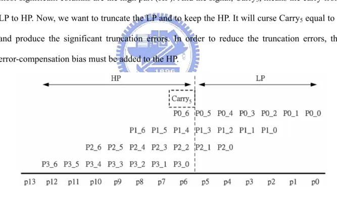
(16) Carry5 = 2−1 ( P0 _ 5 + P1_ 3 + P2 _1 ) + 2−2 ( P0 _ 4 + P1_ 2 + P2 _ 0 ) +2−3 ( P0 _ 3 + P1_1 ) + 2−4 ( P0 _ 2 + P1_ 0 ) −5. (2.1). −6. +2 P0 _1 + 2 P0 _ 0. In general, Equation (2.1) can be written as Equation (2.2). The value of τ means the number of columns of LP which will be truncated.. Carryτ −1 = 2−1 ( P0 _ τ −1 + P1_τ −3 + +2−2 ( P0 _ τ − 2 + P1_τ − 4 + +. + P⎡⎢τ / 2⎤⎥ −1_1 ) + P⎢⎡τ / 2⎥⎤ −1_ 0 ). + 2− (τ −1) P0 _1 + 2−τ P0 _ 0. (2.2). = ⎢⎣ 2−1 β + λ ⎥⎦ As seen in Equation (2.2), the carry is composed of β and λ.. β = P0 _τ −1 + P1_τ −3 +. + P⎡⎢τ / 2⎤⎥ −1_1. λ = 2−2 ( P0 _τ − 2 + P1_τ − 4 +. + P⎢⎡τ / 2⎥⎤ −1_ 0 ) +. + 2− (τ −1) P0 _1 + 2−τ P0 _ 0. (2.3). Where ⎡⎢ x ⎤⎥ represents the smallest integer that is larger than or equal to the number x. The value of β means the total number of “1” in the (τ - 1)th column. If the value of λ can be expressed in terms of β and τ, the error-compensation bias can be obtained in terms of only β and τ. Before we introduce the process of S-J Jou approach, we assume that the probability of each input data bit equaling “1” is 0.5 and the probability of each partial product bit Pi_j equaling “1” is P(Pi_j). According to the P(Pi_j) concept, the equation of λ can be rewritten as 1 ⎡τ − k ⎤ × P( Pi _ j ) × ⎢ k +1 ⎢ 2 ⎥⎥ k =1 2. τ −1. λ =∑. (2.4). The values of P(Pi_j) are different for different β and τ. By using statistical analysis and linear regression line analysis, P(Pi_j) can be approximated as a first-order polynomial.. P ( Pi _ j ) =. 0.41. τ. × β + 0.58(0.01×τ + 0.37). (2.5). Taking Equation (2.4) and Equation (2.5) into Equation (2.3), the error-compensation bias can -5-.
(17) be obtained by Equation (2.6). ⎢ ⎥ ⎧ τ −1 1 ⎡ 0.41 ⎡τ − k ⎤ ⎤ ⎫ Carryτ −1 = ⎢ 2−1 β + ⎨∑ k +1 ⎢ β + 0.58(0.01τ + 0.37) ⎢ ⎬ + 0.5⎥ ⎥ ⎥ ⎢ 2 ⎥⎦⎭ ⎩ k =1 2 ⎣ τ ⎣ ⎦. (2.6). The probable values of Carryτ - 1 f or different τ are listed in Table 2-1. It is obviously that the best error-compensation bias is β for any τ. Table 2-1: Probable values of Carryτ-1 with different values of β and τ. τ. β +2. β +1. β. β −1. β −2. β −3. Expected Value. 85.94%. 11.72%. 0. 0. β - 0.09. 1.27%. 36.35% 56.88%. 5.49%. 0. 0. β + 0.33. 8. 2.11%. 37.06% 53.05%. 7.75%. 0.04%. 0. β + 0.33. 10. 3.23%. 36.78% 50.30%. 9.54%. 0.14%. 0. β + 0.33. 12. 4.38%. 36.24% 47.97%. 11.09%. 0.31%. 3.58E-7. β + 0.33. 14. 5.52%. 35.66% 45.88% 12.38%. 0.55%. 1.20E-5. β + 0.33. 4. 0. 6. 2.34%. Fig 2-3: 6 x 8 fixed-width multiplier with S-J Jou approach. -6-.
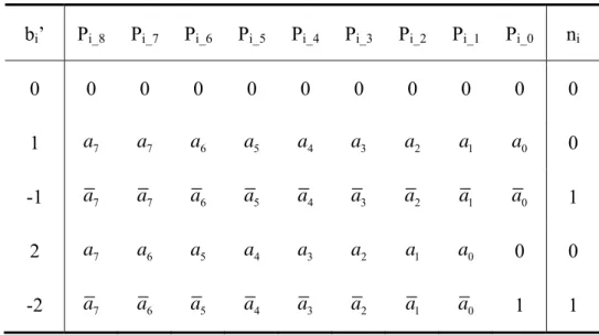
(18) The circuit of 6 x 8 fixed-width Booth multiplier with S-J Jou approach is shown in Fig 2-3. As seen in Fig 2-4, the adder cells of LP are omitted and the carry from LP to HP is replaced by β (P0_5 + P1_3 + P2_1).. 2.2 K-J Cho Approach The S-J Jou approach is introduced in last section. In which, the error-compensation bias is generated using statistical analysis and linear regression analysis. And the probability of each partial product bit Pi_j equaling “1” is different for different β and τ. In this section, the second approach, K-J Cho approach [8] [9], will be introduced. In this approach, the error-compensation bias is obtained by using Booth encoder outputs. And the probability of each partial product bit Pi_j equaling “1” is 1/2 for any β and τ. Table 2-2 shows the values of partial product of 8-bit Booth multipliers. Where bi' = −2ib2i +1 + b2i + b2i −1. (2.4). If the value of bi’ is zero, each bit of partial product “Pi” will be zero. Otherwise, the value of partial product “Pi” will be based on input data “A”. Table 2-2: Partial product for each encoded yi’ with n = 8. bi’. Pi_8. Pi_7. Pi_6. Pi_5. Pi_4. Pi_3. Pi_2. Pi_1. Pi_0. ni. 0. 0. 0. 0. 0. 0. 0. 0. 0. 0. 0. 1. a7. a7. a6. a5. a4. a3. a2. a1. a0. 0. -1. a7. a7. a6. a5. a4. a3. a2. a1. a0. 1. 2. a7. a6. a5. a4. a3. a2. a1. a0. 0. 0. -2. a7. a6. a5. a4. a3. a2. a1. a0. 1. 1. -7-.
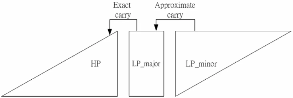
(19) From Fig 2-1, the carry from low part from high part can be expressed as ⎢1 ⎥ Carry7 = ⎢ β + λ ⎥ ⎣2 ⎦. (2.5). β = P0 _ 6 + P1_ 4 + P2 _ 2 + P3_ 0. (2.6). λ = 2−2 ( P0 _ 5 + P1_ 3 + P2 _1 ) + 2−3 ( P0 _ 4 + P1_ 2 + P2 _ 0 + n2 ) + 2−4 ( P0 _ 3 + P1_1 ) + 2−5 ( P0 _ 2 + P1_ 0 + n1 ). (2.7). + 2−6 ( P0 _1 ) + 2−7 ( P0 _ 0 + n0 ). The value of β is sum of the elements in LP_major and the value of λ is the sum of the elements in LP_minor. Fig 2-4 shows the structure of K-J Cho approach. The adder cells of LP_minor are omitted and the error-compensation bias of low part is defined as follow.. ⎡1 ⎤ Carryτ −1 = CE ⎢ β + C A [ λ ]⎥ ⎣2 ⎦. (2.8). Where CE[t] represents the exact carry value of t and CA[t] means the approximate carry value of t. So, CA[λ] means the approximate carry from LP_minor to LP_major.. Fig 2-4: Structure of K-J Cho scheme. In order to find the error-compensation bias, to define yi” as. ⎧1, if yi′ ≠ 0 yi′′ = ⎨ ⎩0, otherwise. (2.9). For example, if the value of y3”y2”y1”y0” is 1000, the coded number y3’y2’y1’y0’ should have -8-.
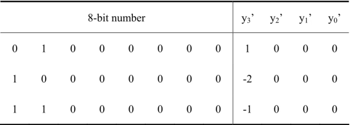
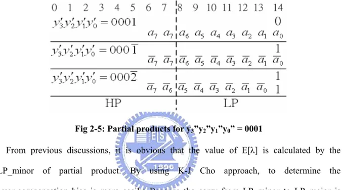
(20) four possible values: 1000, 2000, -1000, and -2000. There are only three 8-bit numbers which can have y3”y2”y1”y0” = 1000. Table 2-3 shows the three 8-bit numbers. Table 2-3: 8-bit numbers with y3”y2”y1”y0” = 1000. 8-bit number. y3’. y2’. y1’. y0’. 0. 1. 0. 0. 0. 0. 0. 0. 1. 0. 0. 0. 1. 0. 0. 0. 0. 0. 0. 0. -2. 0. 0. 0. 1. 1. 0. 0. 0. 0. 0. 0. -1. 0. 0. 0. For the case y3”y2”y1”y0” = 0001, there are also only three possible values of 8-bit numbers, which are shown as follow 00000001(0) → y3′ y2′ y1′ y0′ = 0001 11111110(0) → y3′ y2′ y1′ y0′ = 0002. (2.10). 11111111(0) → y3′ y2′ y1′ y0′ = 000 1. The partial products for the three multiplier coefficients corresponding to y3”y2”y1”y0” = 0001 is shown in Fig 2-5. As we have assumed in last section, the probability of each input bit equaling “1” is 0.5. That is E [ ai ] =. 1 2. (2.11). Thus, the rounded value of E[λ] for each of the three cases in Fig 2-5 can be computed as follows:. {E [λ ]}. r. ⎧0, for y′3 y′2 y1′ y′0 = 0001 =⎨ ⎩ 1, for y′3 y′2 y1′ y′0 = 0002, 000 1. (2.12). Where {t}r means rounding operation for t. In equation (2.12), there are two cases that {E[λ]}r = 1 and one case that {E[λ]}r = 0. In other words, the probability of {E[λ]}r equaling “1” is 2/3 which is bigger than 1/2. So, the -9-.
(21) value of {E[λ]}r can be set to 1 for y3”y2”y1”y0” = 0001. Notice that E[λ] is always zero for the three 8-bit numbers with y3”y2”y1”y0” = 1000. Because no element of the partial product corresponding to y3’ is included in LP_minor as can be seen in Fig 2-1. In general, the element of the partial product corresponding to yn′. 2. −1. is not. included in LP_minor for any input width “n”.. Fig 2-5: Partial products for y3”y2”y1”y0” = 0001. From previous discussions, it is obvious that the value of E[λ] is calculated by the LP_minor of partial product. By using K-J Cho approach, to determine the error-compensation bias is more easily. Because the carry from LP_minor to LP_major is replaced by {E[λ]r}, we only need to calculate the values of {E[λ]r} for each case of y′′n. 2. -2. y′′n. 2. -3. … y0′′ . Then, the circuit of carry generation can be designed based on the values of. {E[λ]r}. The procedure of K-J Cho approach is explained in the following example. Example 1: In this example, it will show the process of K-J Cho approach by using a 10 x 10 Booth multiplier. First, we should calculate the values of {E[λ]}r for all the possible values of y3”y2”y1”y0” and the values of {E[λ]}r are shown in Table 2-4. Notice that y′′4 is not shown in Table 2-4 since there is no any element of the partial product corresponding to y4’ is included in LP_minor. - 10 -.
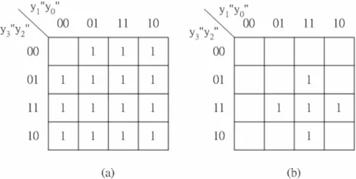
(22) Table 2-4: Rounded value of E[λ] for n = 10. Table 2-5: Representation of approximate carry values. In Table 2-4, the biggest value of carry is two. Thus, two approximate carry signals (LP_carry_0 and LP_carry_1) are needed to represent the values of {E[λ]}r. The values of the two carry signals are shown in Table 2-5. We can obtain the circuit of the approximate carry signals by using Karnaugh map as shown in Fig 2-6. In Fig 2-6, the values of approximate carry signals can be determined using probability analysis. For example, for y3”y2”y1”y0” = 0001, P[{E[λ]}r=0] = 4/12 and P[{E[λ]}r=1] = 8/12. Thus, the value of approximate carry signals is determined to be 1. Then, LP_carry_0 and LP_carry_1 signals can be simplified from each map as LP _ carry _ 0 = y3′′ + y2′′ + y1′′ + y0′′ LP _ carry _1 = y3′′y2′′( y1′′ + y0′′) + y1′′y0′′( y3′′ + y2′′). (2.13). Fig 2-7 shows the circuit of equation (2.13) which is the approximate carry signals from LP_minor to LP_major. The approximate carry signals are added to LP_major. Then, the resulted carry signals from LP_major are added to HP as error-compensation bias. - 11 -.
(23) Fig 2-6: Karnaugh map representation for (a)LP_carry_0 and (b)LP_carry_1 for n = 10. Fig 2-7: Circuit of approximate carry for n = 10. The procedure of Example 1 is illustrated as below: I. For given input width “n”, the number of approximate carry signals is determined as NAC = ⎢⎣ n / 4 ⎥⎦ II. The approximate carry signals are denoted as LP_carry_0, LP_carry_1, … , LP_carry_(NAC - 1) III. To calculate the rounded values of {E[λ]r} for each case of y′′n. 2. -2. y′′n. 2. -3. … y0′′ .. IV. By applying Karnaugh map to the result in step III, approximate carry generation circuit can be designed.. - 12 -.
(24) To perform the exhaustive simulation for large width of input data will take a lot of time. A statistical analysis for obtaining the approximate carry values is introduced as below. Given yi” is 1, it can be shown that E[Pi_j] = 1/2. If y2”y1”y0” = 100 in Fig 2-1, E[λ] can be computed by using equation (2.5) E[λ ] = E[2−1 ( P2 _1 ) + 2−2 ( P2 _ 0 + n2 )] = 2−1 E[ P2 _1 ] + 2−2 ( E[ P2 _ 0 ] + E[n2 ]) = 2−1 (2−1 ) + 2 − 2(2−1 + 2−1 ). (2.14). = 2−1 By the same way, it can be shown that E[λ] is also equal to 1/2 for y2”y1”y0” = 010 and 001. So, for n = 8, E[λ] can be expressed as E[λ ] = 2−1 ( y2′′ + y1′′ + y0′′). (2.15). In general, E[λ] can be computed by equation (2.14) E[λ ] = 2−1 ( yn′′/ 2− 2 + yn′′/ 2−3 + = 2−1 ⋅. n / 2− 2. ∑ i =0. + y0′′). yi′′. (2.16). In the following example, the procedure of this scheme for n = 10 is explained. Example 2: For n = 10 E[λ ] = 2−1 ( y3′′ + y2′′ + y1′′ + y0′′). (2.17). The maximum rounded value of E[λ] is 2. Hence, two signals are needed to represent the rounded value. If the number of yi ” equaling “1” are one or two, the rounded value is equal to 1. Else if the number of yi” equaling “1” are more than three, the rounded value is equal to 2. Then, the approximate carry generation circuit for n = 10 can be obtain as shown in Fig 2-8(a). Using the same scheme, the approximate carry circuit for n = 14 is shown in Fig 2-8(b). - 13 -.
(25) Fig 2-8: Approximate carry generation circuits (a)n = 10 (b)n = 14. The procedure of Example 2 described as below: I. The signals in the { yn′′. 2. −2. yn′′. 2. −3. … y0′′ } are divided into groups of three signals. If the. number of signals in the set is 3N + k (k = 1, 2), the last group contains only k signals. II. The 3N signals are added using N FAs. For k = 2, the two signals in the last group are added using a HA. For k = 1, the signal in the last group is passed to the next stage. The N (or N+1 for k = 2) carry signals from each adder are approximate carry signals. III. The sum signals generated in step II are added using the same principle as in step II. Then, the carry signals from each adder are approximate carry signals. The new sum signals are passed to the next stage. IV. Repeat step II until only one sum signal is left. V. Add “1” to the last adder.. The circuit of 8 x 8 fixed-width multiplier with K-J Cho approach is shown in Fig 2-9. From Fig 2-9, we can find that the adder cells of low part are skipped. The carry from low part to high part is replaced by the approximate carry signals (LP_carry_0 and LP_carry_1) which are generated by Fig 2-8(a).. - 14 -.
(26) Fig 2-9: Fixed-width multiplier with K-J Cho approach for n = 8. 2.3 L-D Van Approach In this section, the fixed-width multiplier proposed by L-D Van will be introduced [10] [11]. The L-D Van approach is based on Baugh-Wooley Array multiplier [12]. Fig 2-10 shows the partial product of 8-bit Baugh-Wooley Array multiplier. It can be divided into two parts, HP and LP, as the same as Booth multiplier.. Fig 2-10 Partial product of 8-bit Baugh-Wooley Array multiplier. In general, the carry from low part to high part of Baugh-Wooley Array multiplier can be defined as Equation (2.18). The two elements, β and λ, are represented in equation (2.19) and (2.20), respectively. - 15 -.
(27) ⎡1 ⎤ Carryτ −1 = ⎢ β + λ ⎥ ⎣2 ⎦r. (2.18). β = xn −1 y 0 + xn − 2 y1 + xn −3 y2 + ... + x1 yn − 2 + x0 yn −1. (2.19). λ = 2−2 ( xn − 2 y0 + xn −3 y1 + ... + x0 yn − 2 ) + ... + 2− n x0 y0. (2.20). Before we introduce L-D Van approach, the terminology, θindex,τ, should be indicated. It signifies the binary value of LP_major for different values of τ, where τ means to keep (n + τ) most-significant columns of partial product and to truncate the (τ – 1) least-significant columns. The value of θindex,τ is indicated in Equation (2.21) and the binary parameters qn −1−τ qn − 2−τ … q0 are belong to {0, 1}.. θ index ,τ (qn −1−τ , qn − 2−τ ,..., q0 ) = < xn −1−τ y0 > qn−1−τ + < xn − 2−τ y1 > qn−2−τ +...+ < x0 yn −1−τ > q0. (2.21). Equation (2.22) illustrates the operation of < X > q ⎧ X , if q = 0 < X >q = ⎨ ⎩ X , otherwise. (2.22). In which X means the complement of the binary number X. For n = 8, the 129th index under keeping eight columns, θindex=129,τ=0, can be written as. θindex =129,τ =0 = x7 y0 + x6 y1 + x5 y2 + x4 y3 + x3 y4 + x2 y5 + x1 y6 + x0 y7. (2.23). In the following discussion, two calculated methods of error-compensation bias for τ = 0 will be explained. According to the derivation result in [10], equation (2.18) can be rewritten as 1 Carryτ −1 = θindex ,τ =0 + [ β − θ index ,τ =0 + λ ]r 2 It can be replaced by - 16 -. (2.24).
(28) Carryτ −1 = (< xn − 2 y1 > qn−2 + < xn −3 y2 > qn−3 +...+ < x1 yn − 2 > q1 ) + [ K ]r. (2.25). 1 K =< xn −1 y0 > qn−1 + < x0 yn −1 > q0 + β − θindex ,τ =0 + λ 2. (2.26). In Equation (2.25), the first term can be easily determined while the index is decided. And the second term, [K]r, can be approached by the expected value which can obtain by full search. In order to get more accurate error-compensation bias, two types of carry-estimation formula are proposed. The formulas are shown in Equation (2.27) and (2.28), separately. ⎧ (< xn − 2 y1 > qn−2 + < xn −3 y2 > qn−3 + Carrytype1 = ⎨ qn − 2 qn−3 ⎩(< xn − 2 y1 > + < xn −3 y2 > + ⎧ (< xn − 2 y1 > qn−2 + < xn −3 y2 > qn−3 + Carrytype 2 = ⎨ qn−2 qn−3 ⎩(< xn − 2 y1 > + < xn −3 y2 > +. + < x1 yn − 2 > q1 ) + [ K1 ]r , if θindex =0 + < x1 yn − 2 > q1 ) + [ K 2 ]r , if θ index >0. + < x1 yn − 2 > q1 ) + [ K 3 ]r , if θindex <n + < x1 yn − 2 > q1 ) + [ K 4 ]r , if θ index =n. (2.27). (2.28). Where K1, K2, K3, and K4 are the average value of K for different range of θindex By full search simulation, we can get the values of K1 and K2 for each index. In order to reduce the complexity of circuit design, to choose the indices which satisfy [K1]r ∈ {0, 1} and [k2]r ∈ {0, 1} is a good idea. For the 6 x 6 multiplier, there are three indices to satisfy the conditions, [K1]r ∈ {0, 1} and [k2]r ∈ {0, 1}. However, these indices do not always satisfy the conditions while the width “n” is changed. In order to find the fixed value of K for different width “n”, the second approach “Type 2” is proposed. By using exhaustive search simulation generated from n = 4 to n = 12, we can find that the specific index θindex = 2n−1 +1 is satisfy [K3]r = 1 and [k4]r = 0. Because the error-compensation bias is shown as Equation (2.25) and. θindex = 2. n−1. +1. = xn −1 y0 + xn − 2 y1 + … + x1 yn − 2 + x0 yn −1 , it can be described as Equation. (2.29) for n ≤ 12.. - 17 -.
(29) ⎧ (< xn − 2 y1 > qn−2 + < xn −3 y2 > qn−3 + ⎪ ⎪ CarryType 2,index = 2n−1 +1 = ⎨ qn−2 q n −3 ⎪(< xn − 2 y1 > + < xn −3 y2 > + ⎪ ⎩. + < x1 yn − 2 > q1 ) + 1, if θ index=2n-1 +1 <n + < x1 yn − 2 > q1 ),. (2.29). if θindex=2n-1 +1 =n. To perform the exhaustive simulation for large width “n” will take a lot of time. In the following discussion, “Type 2” approach for large width “n” will be introduced. Two cases of “Type 2” approach,. θindex = 2. n−1. +1. < n and. θindex = 2. n −1. +1. = n will be explained, separately.. Case 1: θindex = 2n−1 +1 < n. We have assumed that the probability of each bit of input data equaling “1” is 1/2. Hence, the value of E[ xi y j ] and E[ xi y j ] are equal to 1/4 and 3/4. According to the values of E[ xi y j ] and E[ xi y j ] , the expected value of. 1 β can be represented as 2. 1 1 ⎛3 3 1 ⎞ E[ β ] = × ⎜ + + × (n − 2) ⎟ 2 2 ⎝4 4 4 ⎠ n 1 = + 8 2. (2.30). Similarly, the expected value of λ can be shown as 1 1 1 1 1 1 × × (n − 1) + 3 × × (n − 2) + + n × × 1 2 2 4 2 4 2 4 1⎛ 1 1 1 ⎞ = ⎜ 2 × (n − 1) + 3 × (n − 2) + + n + 1⎟ 4⎝2 2 2 ⎠ n 1 ≅ − , if n ≥ 4 8 4. E[λ ] =. From equation (2.26), the value of [K3]r for index = 2n-1 + 1 is indicated as. - 18 -. (2.31).
(30) [ K 3 ]r = [ E[ K ]]r 1 ⎡ ⎤ = ⎢ E[ xn −1 y0 + x0 yn −1 − β + λ ]⎥ 2 ⎣ ⎦r ⎡3 3 n 1 n 1⎤ = ⎢ + − − + − ⎥ =1 ⎣ 4 4 8 2 8 4 ⎦r. (2.32). Hence, we can obtain the error-compensation bias for large width “n” without using exhaustive search scheme. Equation (2.33) shows the error-compensation bias for. θindex = 2. n−1. +1. < n which is the same as equation (2.29) CarryType 2,index = 2n−1 +1 = (< xn − 2 y1 > qn−2 + < xn −3 y2 > qn−3 +. + < x1 yn − 2 > q1 ) + 1,. if θindex=2n-1 +1 <n. (2.33). Case 2: θindex = 2n−1 +1 = n. The case θindex = 2n−1 +1 = n is met only when x0 yn −1 = xn −1 y0 = 1 and x1 yn − 2 = x2 yn −3 = = xn − 2 y1 = 1. So, the expected value of. 1 β can be represented as 2. 1 1 1 E[ β ] = × 1× n = n 2 2 2. (2.34). And the expected value of λ can be shown as E[λ ] =. 1 ⎛1 ⎞ 1 ⎛1 ⎞ × 1× 2 + 1× (n − 3) ⎟ + 2 ⎜ × 1× 2 + 1× (n − 4) ⎟ 2 ⎜ 2 ⎝3 ⎠ 2 ⎝3 ⎠ +. =. +. 1 ⎛1 ⎞ 1 ⎛1 ⎞ × 1 × 2 ⎟ + n ⎜ × 1× 1 ⎟ n -1 ⎜ 2 ⎝3 ⎠ 2 ⎝9 ⎠. (2.35). 1 5 n − , if n ≥ 4 2 3. According to Equation (2.34) and (2.35), the value of [K4]r for index = 2n-1 + 1 is illustrated in Equation (2.36).. - 19 -.
(31) [ K 4 ]r = [ E[ K ]]r. (2.36). 1 ⎡ ⎤ = ⎢ E[ xn −1 y0 + x0 yn −1 − β + λ ]⎥ = 0 2 ⎣ ⎦r. The error-compensation bias for case 2 is shown in Equation (2.37) which is the same as Equation (2.29) CarryType 2,index = 2n−1 +1 = (< xn − 2 y1 > qn−2 + < xn −3 y2 > qn−3 +. + < x1 yn − 2 > q1 ),. if θindex=2n-1 +1 =n. (2.37). Fig 2-11 shows the circuit of 8-bit fixed-width multiplier with the 129th index. The function of A-A cell is to judge whether the value of θindex = 2n−1 +1 is equal to n or not.. Fig 2-11: Fixed-width multiplier with L-D VAN approach for n = 8 - 20 -.
(32) Chapter3 Proposed Self-Compensation Multiplier In chapter 2, three existed Fixed-width multiplier are introduced, S-J Jou approach, K-J Cho approach, and L-D Van approach. S-J Jou approach and K-J Cho approach are based on Booth multiplier and the L-D Van approach is based on Baugh-Wooley Array multiplier. In this chapter, a new approach of fixed-width multiplier which is based on Booth multiplier will be introduced. The error-compensation bias of proposed approach is produced by the carry-estimation equations. In order to reduce the truncation error, the carry-estimation equations are adapted for n = 8 to n =16. These equations for different n can be analyzed by few logic gates. Hence, the circuit complexity of proposed approach is closed to direct-truncation approach. The error-compensation bias is introduced in section 3.1 and the circuit of proposed structure is illustrated in section 3.2. Finally, the comparison of performance for each approach is shown in section 3.3.. 3.1 Calculation of Error-compensation bias Fig 3-1 shows the partial product of 8-bit Booth multiplier and the partial product is divided into two parts, low part (LP) and high part (HP). The LP can be further divided into two parts, the first column of LP is LP_major and the remaining columns of LP are LP_minor. The carry-out bit from LP to HP is written as equation (3.1), where β the sum of LP_major and λ is the sum of LP_minor. ⎢1 ⎥ Carry7 = ⎢ β + λ ⎥ ⎣2 ⎦ - 21 -. (3.1).
(33) β = P0 _ 7 + P1_ 5 + P2 _ 3 + P3_1. (3.2). λ = 2−2 ( P0 _ 6 + P1_ 4 + P2 _ 2 + P3_ 0 + n3 ) + 2−3 ( P0 _ 5 + P1_ 3 + P2 _1 ) + 2−4 ( P0 _ 4 + P1_ 2 + P2 _ 0 + n2 ) + 2−5 ( P0 _ 3 + P1_1 ) + 2−6 ( P0 _ 2 + P1_ 0 + n1 ) + 2−7 ( P0 _1 ). (3.3). + 2−8 ( P0 _ 0 + n0 ). In order to find the error-compensation bias, LP_major index, θ, is defined as equation follow.. θ = P0 _ 7 + 21 i P1_ 5 + 22 i P2 _ 3 + 23 i P3_1 the values of θ for different values of LP_major are shown in Table 3-1. Table 3-1: The values of θ for different values of P3_0P2_2P1_4P0_6. Fig 3-1: Partial product of 8-bit Booth multiplier - 22 -. (3.4).
(34) It is obviously that if one value of θ is selected, the value of β is fixed. For example, if the value of θ is equal to 7, the value of β must be equal to 3. We can obtain the average carry for each value of θ by using full search simulation. Because the value of β is fixed, we only need to calculate the average carry from LP_minor to HP (λ). The results of full search simulation for n = 8 are represented in Table 3-2. Table 3-2: The average carry for each value of θ. Now, we can get the error-compensation bias by using look-up table method. The input of table is the four elements of LP_major and three approximate carry signals are needed to represent the values of error-compensation bias. The block diagram of error-compensation bias is illustrated in Fig 3-2.. Fig 3-2: The error-compensation table for n = 8. - 23 -.
(35) As mentioned in former discussion, the values of approximate carry signals are obtained by looking up table. But the area of error-compensation table will increase when n is large. Hence, it is unwise to obtain the error-compensation bias by this method. The new approach should be proposed to improve the hardware complexity of look-up table method. In order to find the new approach, we try to find the rule between average carry and θ. Fortunately, the average carry is related to the number of “1” in LP_major which is the value of β. If the values of θ have the same number of “1” in LP_major, the values of average carry for these θ will be all equally. For example, the values of average carry are all equal to 1 for θ = 1, 2, 4, and 8 in which the number of “1” in LP_major is all equal to 1. The relation between average carry and the number of “1” in LP_major is shown in Table 3-3 for n= 8. Table 3-3: The values of Average carry for each β for n = 8. From Table 3-3, we can derive a carry-estimation equation which can computed the average carry for n = 8. The carry-estimation equation is written as. ⎢β ⎥ Carry7 = ⎢ ⎥ + 1 ⎣2⎦. (3.5). The results of this equation are the error-compensation bias for n = 8. Table 3-4 shows the results of carry-estimation equation for n = 8. - 24 -.
(36) Table 3-4: The results of carry-estimation equation for n = 8. As seen in Table 3-4, the results of carry-estimation equation are all equal to the values of average carry which are obtain by full search simulation. Hence, we can calculate the error-compensation bias by equation (3.5). The carry-estimation equations for different width “n” can be obtained by similarly process. Equation (3.6) and equation (3.7) show the carry-estimation equations for n = 10 to n = 16. And the results of these carry-calculate equations are represented in Table 3-5.. Carryn. 2. −1. ⎢ β + 1⎥ =⎢ + 1, for n = 10, 12, and 14 ⎣ 2 ⎥⎦. ⎢β ⎥ Carry15 = ⎢ ⎥ + 2, for n = 16 ⎣2⎦. (3.6). (3.7). However, the values of carry-estimation equations do not always match the values of average carry. For example, the result of carry-estimation equation is equal to 2 for n = 10 and β = 1. But the value of average carry is equal to 1. In order to derive the influence of the truncation error caused by this inequality situation, the probability of the mismatch situation is calculated. First, the number of cases for each value of β is computed. Equation (3.8) shows the equation which can calculate the number of cases for each β.. N β = Cβn 2. - 25 -. (3.8).
(37) Table 3-5: The results of carry-estimation equation for (a) n = 10 (b) n = 12 (c) n = 14 (d) n = 16. Table 3-6 shows the numbers of cases for each β with n = 10. It is obviously that, the probability of β equaling “1” is only 5 condition is only 5. 32. 32. . In other words, the probability of the mismatch. (15%) for n = 10. Thus, the increase of the truncation error caused by. the mismatch situation will be few.. - 26 -.
(38) Table 3-6: The numbers of cases for each β with n = 10. Similarly, the mismatch condition occurs for β = 6 and n = 14. We can also find the number of cases for each β by using equation (3.8). Table 3-7 shows the numbers of cases for each β with n = 14. In Table 3-7, we can see that the probability of β equaling “6” is only 7 probability of the mismatch condition is only 7. 128. 128. . That is, the. (5.4%). Hence, the increase of the. truncation error caused by inequality condition is also very little for n = 14. Table 3-7: The numbers of cases for each β with n = 14. The inequality situation is also occurred for n = 16. There are two conditions, β = 0 and β = 2, that the results of carry-estimation equation are not equal to average carry. By using equation (3.8), the numbers of cases for each β with n = 16 can be obtained from Table 3-8. Table 3-8: The numbers of cases for each β with n = 16. The probability of the inequality condition is only 11%. Hence, the increase of the truncation error for n =16 is still very little. In former discussion, we can know that the error-compensation bias can be obtained by using the carry-estimation equations for n = 8 to n = 16. And the results of the - 27 -.
(39) carry-estimation equations are almost the same as average carry which is obtained by full search simulation.. 3.2 Proposed Structure In this section, the circuits of carry-estimation equations for n = 8 to n = 16 are introduced. The carry-estimation equation for n = 8 is shown in equation (3.5) which is composed by ⎢ β ⎥ and “plus 1”. The function of ⎢ β ⎥ can be calculated by the carry of LP_major. ⎢⎣ 2 ⎥⎦ ⎢⎣ 2 ⎥⎦ The process of calculation of ⎢ β ⎥ is shown as follow. First, the elements of LP_major are ⎢⎣ 2 ⎥⎦ summed by some full adders and half adders. The carry signals from each adder are the carry from LP_major to HP, and the sum signals are added. The new carry signals from the added sum signals are also the carry from LP_major to HP. Repeat former steps until only one sum signal is left. As regards the function of plus “1”, we only need to assign the third carry signal “Carry[2]” equal to 1 for n = 8. Fig 3-3 illustrates the circuit of carry-estimation equation for n = 8.. Fig 3-3: Circuit of carry-estimation equation for n = 8. As seen in Fig 3-3, the circuit only needs one full adder and one half adder. Thus, the penalty of area for computed error-compensation bias is very small. Fig 3-4 illustrates the circuit of 8-bit Booth multiplier with proposed approach. In Fig 3-4, - 28 -.
(40) the adder cells required for LP are all omitted, and the carry-out from LP to HP is estimated by equation (3-5) which corresponds to Carry[0], Carry[1], and Carry[2] in Fig 3-4. There are eight full adders, seven half adders, and one 8-bit CPA in this multiplier. The ratio of area between the circuit of carry-estimation equation and the circuit of 8 x 8 booth multiplier is very small. Thus, the area of proposed multiplier is only a bit larger than the area of direct-truncated multiplier.. Fig 3-4: Circuit of 8-bit Booth multiplier with proposed approach. Fig 3-5 shows the circuits of carry-estimation equations for n =10 to n = 16. We can see that the required adders do not increase much as the width “n” increases. The required adders are three full adders for n = 12. Even for n = 16, the required adders are only four full adders which are one more full adder than the condition of n = 12. According to the few required adders for large width “n”, the influence of the increased area coursed by the circuit of carry-estimation equation can be skipped for large width “n”. Thus, the ratio of area between proposed multiplier and direct-truncated multiplier is almost equal to “1” for large width “n”. That is, the area of proposed approach is close to the area of direct-truncated multiplier.. - 29 -.
(41) Fig 3-5: Circuits of carry-estimation equations for (a) n = 10 (b) n = 12 (c) n = 14 (d) n = 16. - 30 -.
(42) 3.3 Performance Analysis The performance of different approaches will be represented in this section. The performance is evaluated in terms of average error, the variance of errors, and gate count. Note that the comparison of gate counts only contains the approach based on Booth multiplier. However, the approach proposed by L-D Van [11] is based on Baugh-Wooley Array multiplier, it does not include in the comparison of gate counts. The absolute error between the standard Booth multiplier and fixed-width multiplier is defined as. ε = PStandard − PFixed-width. (3.9). where Pstandard represents the computational result of standard Booth multiplier and PFixed-width represents the result of fixed-width multiplier. The average error is defined as equation (3.10) where E[ x] is the expected value of x.. ε = E[ε ]. (3.10). Besides the comparison of average error, the variance of error for each approach is compared, too. The computation of the variance of error is described as equation (3.11).. ν = E[(ε − ε ) 2 ]. (3.11). It is obvious that the fixed-width multiplier with smaller truncation error has more accurate results. Similarly, the approach with smaller variance of error has stable results. The comparison of average error and the variance of error are represented in Table 3-9 and Table 3-10, respectively. And the comparison of gate counts is shown in Table 3-11. From Table 3-9, the error of proposed approach is only 11% of direct-truncated multiplier for n = 16. Besides average error, the variances of our multiplier are only 4.9% of direct-truncated multiplier. It means that the proposed approach is more stable than direct-truncated multiplier. - 31 -.
(43) The comparisons of gate counts are based on Booth multiplier. The gate count of proposed approach is a bit larger than S-J Jou approach but is smaller than K-J Cho approach. For large width “n”, the gate count of our approach is very close to S-J Jou approach, because the number of adder for carry-estimation equation is very small. In conclusion, the proposed approach has three features: I. Low average error II. More stable than other approach III. Area efficient. Table 3-9: Comparison results of average error. - 32 -.
(44) Table 3-10: Comparison results of variance of error. Table 3-11: Comparison results of gate counts. - 33 -.
(45) Chapter4 Application of Fixed-Width Multipliers in FFT The low-error area efficient fixed-width multiplier is proposed in chapter 3. The average error of proposed structure is only about 15% of direct-truncated multiplier. As well as the area of proposed one is only about 60% of standard Booth multiplier. In order to reduce the hardware complexity, the multiplication operations in FFT usually have the fixed-width property. Thus, the proposed fixed-width multiplier is employed in the 128-point FFT architecture [13]. The truncation errors will be introduced because of the usage of the fixed-width multiplier and it will decrease the performance of the 128-point FFT. In section 4.1, the 128-point FFT algorithm will be introduced. Then the architecture of 128-point FFT will be introduced in section 4.2. Finally, the performance of 128-point FFT is shown in section 4.3.. 4.1 Introduction to 128-Point FFT In this section, the 128-point FFT algorithm proposed by Y-W Lin [13] will be introduced. Given a sequence x(n), the N-point DFT is defined as N. X (k ) = ∑ x(n)WNkn (k = 0,1,. , N − 1). (4.1). n=0. Where x(n) and X(k) are complex numbers. And the values of WNkn is WNnk = cos(2π nk. N. ) − j sin(2π nk. N. ). (4.2). In equation (4.1) the computational complexity is O( N 2 ) through directly performing the. - 34 -.
(46) required computation. The computational complexity can be reduced to O( N log rN ) by using the radix-r FFT algorithm. In general, higher-radix FFT algorithm has less number of complex multiplications while compared with radix-2 FFT algorithm. Hence, the radix-8 FFT algorithm is employed in the 128-point FFT. But the 128-point FFT is not the power of 8, the mixed-radix FFT algorithm which include radix-2 FFT and radix-8 FFT algorithm should be chosen. The mixed-radix 128-point FFT algorithm is derived as below. First, let the constant in equation (4.1) as N = 128. ⎧ n = 0,1 n = 64n1 + n2 ⎨ 1 ⎩n2 = 0,1, , 63 ⎧k = 0,1 k = k1 + 2k2 ⎨ 1 ⎩ k2 = 0,1, , 63. (4.3). Then, equation (4.1) can be rewritten as X (2k2 + k1 ) =. 63. 1. ∑ ∑ x(64n + n )W 1. n2 = 0 n1 = 0. 2. (64 n1 + n2 )(2 k2 + k1 ) 128. ⎧ ⎫ ⎪⎪ 1 ⎪ nk n2 k1 ⎪ = ∑ ⎨ ∑ x(64n1 + n2 )W2n1k1 W128 ⎬W642 2 n2 = 0 ⎪ n1 = 0 twiddle factor ⎪ ⎪⎩ ⎪⎭ 2 po int DFT 63. (4.4). 64 po int DFT. =. 63. ∑ BU. n2 = 0. 2. (k1 , n2 )W64n2 k2. In equation (4.4), the 128-point DFT can be considered as a two-dimensional DFT, 2-point DFT and 64-point DFT. The inputs of 128-point DFT are computed by radix-2 FFT algorithm at first. Then, the results of radix-2 FFT are multiplied by twiddle factor. Finally, the results of multiplication should be calculated by 64-point DFT algorithm which can decomposed into 8-point DFT recursively 2 times. In order to derived the 64-point FFT algorithm by using radix-23 FFT algorithm, the constant n2 and k2 in equation (4.3) can be defined as - 35 -.
(47) n2 = 32α1 + 16α 2 + 8α 3 + α 4 , α1 , α 2 , α 3 = 0,1;α 4 = 0,1,. ,7. k2 = β1 + 2β 2 + 4β 3 + 8β 4 ,. ,7. β1 , β 2 , β3 = 0,1; β 4 = 0,1,. (4.5). Using equation (4.5), equation (4.4) can be rewritten as X ( 2( β1 + 2β 2 + 4β3 + 8β 4 ) + k1 ) = 7. 1. 1. 1. ∑ ∑ ∑ ∑ BU. α 4 = 0 α 3 = 0 α 2 = 0 α1 = 0. 2. (k1 ,32α1 + 16α 2 + 8α 3 + α 4 ). (4.6). ×W64(32α1 +16α 2 +8α3 +α 4 )( β1 + 2 β2 + 4 β3 +8 β4 ) Where the twiddle factor can be decomposed as W64(32α1 +16α 2 +8α3 +α 4 )( β1 + 2 β2 + 4 β3 +8 β 4 ) =. (4.7). W2α1β1W4α 2 β1W2α 2 β2W8α3 ( β1 + 2 β2 )W2α3β3W64α 4 ( β1 + 2 β 2 + 4 β3 )W8α 4 β4. Thus, equation (4.6) becomes X ( 2( β1 + 2β 2 + 4β 3 + 8β 4 ) + k1 ) =. 7. ∑ BU (k , β , β , β ,α α 8. 4 =0. 1. 1. 2. 3. 4. )W8α 4 β4. (4.8). Where BU 8 (k1 , β1 , β 2 , β3 , α 4 ) = ⎧ ⎫ ⎪ ⎪ 1 1 1 ⎪ α 3 ( β1 + 2 β 2 ) α 3 β3 α 4 ( β1 + 2 β 2 + 4 β3 ) ⎪ α1β1 α 2 β1 α 2 β2 W2 W64 ⎬ ∑∑∑ ⎨ BU 2 (k1 , α1 ,α 2 , α3 , α 4 )W2 W4 W2 W8 α 3=0 α 2=0 α1=0 ⎪ ⎪ 1st step ⎪⎩ ⎪⎭ 2 nd step. (4.9). 3 rd step. In equation (4.9), the 8-point DFT are divided into three steps by using radix-2 index map. Fig 4-1 shows the signal flow graph of the radix-8 FFT algorithm. In which, the radix-8 algorithm is decomposed into three steps. Each step has four butterfly operations. After the butterfly operations, the multiplications of twiddle factors in each step should be performed. There are only three twiddle factors, -j, W81 , and W83 in radix-8 algorithm. The multiplication of “-j” only needs to exchange the real part with imaginary part. Thus, it does not need any multiplier. The multiplications of the twiddle factors, W81 and W83 , can be - 36 -.
(48) replaced by some additions. Because the twiddle factors can be written as −. (. ). 2 2 (1 − j ) , respectively. The value of. 2 2 (1 − j ) and. 2 2 is equal to 0.70710678 which can be. written as 2−1 + 2−3 + 2−4 + 2−6 + 2−8 can be complemented only by five shifters and four adders .. Fig 4-1: The signal flow graph of radix-8 FFT algorithm. The signal flow graph of 128-point mixed-radix FFT algorithm is shown as Fig 4-2. In which, the 128-point FFT is composed by three stage. The first stage is performed by radix-2 FFT algorithm and the radix-8 FFT algorithm shown in Fig 4-1 is employed in the second and third stages. The black point in each stage means that one twiddle factor will be multiplied at that point. In the first stage, there are sixty-four butterfly units and the two inputs of ith butterfly unit are ith and (64+i)th input data where i = 0 ~ 63. Then the results of first stage should be calculated by the second and third stages. There are sixteen radix-8 FFT units in the second and third stages, respectively. The orders of radix-8 FFT inputs are different in each stage. In the second stage, the inputs of each radix-8 FFT unit are shown as below ⎧(64i + j )th , (64i + j + 8)th , (64i + j + 16)th , (64i + j + 24)th , ⎫ ⎨ ⎬ ⎩(64i + j + 32)th , (64i + j + 40)th , (64i + j + 48)th , (64i + j + 56)th ⎭ i = 0,1; j = 0,1,. , 7;. for (8i + j )th radix - 8 FFT unit. But in the third stage, the eight inputs are (8i)th ~ (8i + 7)th input data for i = 0 ~ 15. - 37 -. (4.10).
(49) Fig 4-2: The signal flow graph of 128-point mixed-radix FFT algorithm. 4.2 128-Point FFT Architecture In order to reduce the area of 128-point FFT, the proposed multiplier is employed in the 128-point FFT architecture. The 128-point FFT architecture proposed by Y-W Lin’s [13] is introduced in this section. Fig 4-3 shows the 128-point FFT architecture which is divided into three modules. The first - 38 -.
(50) module is complemented by radix-2 FFT algorithm, and the radix-8 FFT algorithm is used in the second and the third modules. In this architecture, the high throughput rate is achieved by using four parallel data paths; the order of the output sequence is the bit reversal of the order of the input sequence as seen in Fig 4-3.. Fig 4-3: Block diagram of 128-point FFT. 4.2.1 Module 1 Fig 4-4 shows the architecture of Module 1 which consists of 128 registers which can store 64 complex data, four two-input butterfly units (BU), two complex multipliers, and two ROMs. The ROMs are used to store the twiddle factors. The 128 registers are used to store inputs data and the outputs of BU. The operations of BU are the complex addition and the complex subtraction from two input data. Because the two inputs of each BU are in(i) and in(64+i) where i is from 0 to 63. This is corresponds to the first stage of Fig 4-2. The order of four parallel input sequences in Module 1 is in(4m), in(4m+1), in(4m+2), and in(4m+3) where m is from 0 to 31. Thus, the 64 input data at first 16 cycles should be stored in the register file. At next 16 cycles, the eight inputs of the four BU are received from the register file and the inputs data, respectively. Then eight outputs data are generated by the four BU. The four outputs of the complex addition are sent to the Module 2 directly, and the other four outputs of complex subtraction are stored in the register file. Before the four outputs are stored, two of them are multiplied by twiddle factors. After 32 cycles, the other two outputs are multiplied - 39 -.
(51) by twiddle factors. Then, the four outputs are fed into the Module 2. By this multiplication approach can not only reduce the four complex multipliers to two complex multipliers but also achieve 100% utilization of the complex multipliers.. Fig 4-4: Block diagram of the Module 1. 4.2.2 Module 2 The block diagram of the Module 2 is illustrated in Fig 4-5. It consists of four BU_8 structures and four complex multipliers. The architecture of BU_8 is directly mapped from 3-step radix-8 FFT algorithm as seen in Fig 4-1. And the numbers of registers in each step are eight, four, and tow, respectively. These registers are used to store the input of two-input BU until the other available input is received. The outputs of two-input BU in first and second steps should be multiplied by the twiddle factors, 1, -j, W81 , and W83 . As mentioned in Section 4.1, the multiplications of these twiddle factors can be implemented without any multipliers. But the four outputs of BU_8 need to be multiplied by the nontrivial twiddle factors with four complex multipliers.. - 40 -.
(52) Fig 4-5: Block diagram of the Module 2. 4.2.3 Module 3 The Module 3 is also realized by radix-8 FFT algorithm. Fig 4-6 shows the block diagram of the Module 3. The structure of the Module 3 is different from that of Module 2, because the orders of input data of the Module 2 and the Module 3 are different. The structure should be adapted for the different orders of output as shown in Fig 4-6. The outputs data in first and second steps only need to be multiplied by the twiddle factors, 1, -j, W81 , and W83 . Thus, no any multiplier is used in the Module 3.. Fig 4-6: Block diagram of the Module 3. - 41 -.
(53) 4.3 Simulation Results The algorithm and architecture of 128-point FFT are introduced in section 4.1 and section 4.2, respectively. In this section, the performance of 128-point FFT will be represented. Table 4-1 shows the SQNR of different 128-point FFT approaches. The first column indicates what kinds of multipliers are used in the 128-point FFT architecture. “Booth” means the traditional Booth multiplier; “Direct_t” means the direct-truncated multiplier; and “Proposed” means the 128-point FFT with proposed multiplier. The first row shows the width of twiddle factors and input data. Because there are 2 bits right of decimal point of twiddle factors. The truncation-bit is only n - 2 bits. For example, if the width of twiddle factors is 10, the truncation-bit is only 8 bits which are left of decimal point. In Table 4-1, the SQNR of proposed approach is only 1dB less than the traditional Booth multiplier. But it is about 10dB larger than the direct-truncated multiplier. Table 4-1: SQNR of 128-point FFT with different multiplier approach. Table 4-2 represents the gate count of 128-point FFT with the three different multipliers for n = 10. Compare to the traditional Booth multipliers, our approach improves by 10% reduction in gate count. And it is only 2% bigger than the direct-truncated multiplier. As mentioned in section 4.1, the 128-point mixed-radix FFT algorithm is divided into three stages. The multiplications of twiddle factors should be performed in the end of each stage. In Fig 4-2, the multiplications should be performed in the end of first stage and the end of second stage. Because the fixed-width multipliers which cause the truncation errors are - 42 -.
(54) employed, the multiplications of twiddle factors will reduce the performance of FFT. The computations of twiddle factors will increase, if the points of FFT are raised. Thus, the more point of FFT is needed; the less performance will be expected. In order to observe the performance of high-point FFT by using Fixed-width multipliers, the proposed approach is employed in the 8192-point FFT algorithm [14]. Table 4-3 shows the simulation results of 8192-point FFT. The SQNR of proposed approach is about 2dB less than the standard Booth multiplier. But it is still larger than the direct-truncated multiplier approach.. Table 4-2: Gate count of 128-point FFT for n = 10. Table 4-3: SQNR of 8192-point FFT with different multiplier approach. - 43 -.
(55) Chapter5 Implementation Results for 128-point FFT This chapter will describe the CHIP implementation and its design methodology. In section 5.1, the implementation of 128-point FFT with proposed multiplier is introduced. In section 5.2, the implementation of approach 2 is described. The architecture of approach 2 is the same as approach 1. But the registers of approach 2 are replaced by DDR (Double Data Rate) registers can catch data not only in positive edge clock but also in negative edge clock. The function of DDR registers will be introduced in section 5.2. Finally, the simulation result of two proposed architecture are represented in section 5.3.. 5.1 Approach 1 The proposed approach 1 implements the 128-point FFT architecture with proposed fixed-width multiplier. The structure of approach 1 has been described in section 4.2. The width of input data and twiddle factors are 10-bit and the width of output data is 14-bit. In order to avoid the overflow of computations of BU, the outputs of BU is 1-bit larger than the inputs of BU. In the 128-point FFT algorithm, seven computations of BU are needed. Thus, the outputs of 128-point FFT are 7-bit larger than the inputs. In the cause of low hardware complexity, the least significant 3-bit of the four outputs of stage2 as seen in Fig 4.3 are truncated. The bits of outputs of first, second, and third stages are, 11-bit, 14-bit, and 14-bit, respectively. As mentioned in section 4.2, four data path is employed in our 128-point FFT architecture. Thus, the 14 x 256-bit SRAM is used to save the chip pins. The inputs data are stored serially in the SRAM from the 10-bit chip input pins before the operation of calculation. Then the four complex data in parallel are fed to the 128-point FFT structure. After the computations of - 44 -.
(56) 128-point FFT, the four complex outputs of 128-point FFT are stored in the SRAM. Finally, the outputs of 128-point FFT are read serially from the SRAM. This 128-point FFT architecture is implemented by 0.18µm one-poly six-metal (1P6M) standard cell technology. Fig 5-1 shows the layout view of approach 1. Table 5-1 shows the chip summary of approach 1. The total gate count is about 164K with test module 81K and the maximum clock rate is 195 MHz. And, the core size is 1.46 x 1.46 mm2. The maximum power consumption is 500mW at clock rate 195 MHz. The chip is packaged in a 128 CQFP package.. Fig 5-1 Layout view of approach 1. - 45 -.
(57) Table 5-1: The chip summary of approach 1 architecture. Memory size. 13 x 256 bits. Core area (mm2). 1.46mm x 1.46mm 83K. Total gate count + 81K Test Module Maximum Operating Frequency. 195 MHz 1.2G*. Date rate (ample/s) 780M** 363mW@300MHz* Average Power 246mW@195MHz** *. Typical Case 1.8V. **. Worst Case 1.62V. 5.2 Approach 2 The structure of approach 2 is almost the same as approach 1 besides the registers. The DDR registers are employed in approach 2. The proposed DDR registers can catch data either at positive edge clock or at negative edge clock. Thus, two operations can be computed during one clock cycle. We can achieve the same throughput rate as D Flip-Flop structure at half operation frequency by using DDR registers. Fig 5.2 shows the structure of DDR register which is composed by two parallel latches. - 46 -.
(58) Fig 5-2: Structure of DDR register. The function of latch is shown in Table 5-2. If OE = 0, the state of the latch is “Z” and the output, Q[n+1], is high impedance. Else if OE = 1 and G = 1, the state of the latch is “Store” and Q[n+1] is equal to input, D. Otherwise, the state of the latch is “Latch” and Q[n+1] is equal to the last output, Q[n]. Table 5-2: Function of Latch. The operation of proposed DDR register at CLK = 0 is shown in Fig 5-3(a). At CLK = 0, the state of Latch 1 is “Latch” and the output, Q1, is equal to Q1[n]. The state of Latch 2 is “Z” and the output, Q2, is high impedance. Thus, the output of proposed DDR register is equal to Q1[n]. By the same way, the state of Latch 1 and Latch 2 are “Z”, and “Latch” respectively when CLK = 1. So, the output of DDR register is equal to Q2[n] . Fig 5-4 is an example of proposed DDR register. And the function of proposed DDR register is described in Table 5-3.. - 47 -.
(59) Fig 5-3: Operations of proposed DDR register at (a) CLK = 0 (b) CLK = 1. Fig 5-4: Example of proposed DDR register. - 48 -.
(60) Table 5-3 Function of proposed DDR register. Approach 2 is also implemented by 0.18µm one-poly six-metal (1P6M) standard cell technology. Fig 5-5 shows layout view of approach 2. Table 5-4 shows the chip summary of approach 2. The total gate count is about 222K with test module 108K, and the maximum clock rate is 90 MHz. Because the DDR registers are employed and the number of data paths is four, the data rate is 720M samples/sec. The core size is 2.24 x 2.24 mm2. The average power consumption is 533mW at clock rate 90 MHz. The chip is packaged in a 128 CQFP package.. - 49 -.
(61) Fig 5-5 Layout view of approach 2 Table 5-4: The chip summary of approach 2 architecture. Memory size. 13 x 256 bits. Core area (mm2). 2.24mm x 2.24mm 113K. Total gate count + 108K Test Module Maximum Operating Frequency. 90 MHz. Date rate (M samples/s). 720. Average Power. 533mW (Include RAM) - 50 -.
(62) 5.3 Comparison Table 5-5 lists the comparisons of various 128-point FFT approaches. The proposed approach is simulated in 0.18µm (1P6M) worst case. From this table, it is obviously that Approach 1 has the minimum core size. And the power is smaller than Booth approach. Table 5-5: Comparison of various 128-point FFT architectures Y-W Lin[13]. K-H Lin[15]. Booth. Approach 1. 0.18μm 1P6M. 0.18μm 1P6M. 0.18μm 1P6M. 0.18μm 1P6M. 10-bit. 8-bit. 10-bit. 10-bit. SQNR. 30dB. 31dB. 33dB. 32dB. Data path. 4. 4. 4. 4. 1.2G sample/s*. 1.2G sample/s*. 1G sample/s. 800M sample/s**. Process Input width. Maximu m. 780M sample/s** 780M sample/s** Data rate 443mW. 336mW. Average. 175mW. 127mW. @300MHz*. @300MHz*. Power. @250MHz. @132MHz**. 286mW. 246mW. @195MHz**. @195MHz** 1.18 x 1.18. Chip size. 1.76 x 1.76. 1.56 x 1.56. (mm2). (include RAM). (include RAM). 1.24 x 1.24. (1.46 x 1.46 include RAM)). * **. Typical Case 1.8V Worst Case. 1.62V. - 51 -.
(63) Chapter6 Conclusion In this paper, the low-error area-efficient fixed-width multiplier is proposed. The proposed fixed-width multiplier can not only reduce the truncation error but also decrease the circuit complexity. The average error of proposed fixed-width multiplier is only 15% of direct-truncated multiplier. And the area of our approach is only 60% of the standard Booth multiplier. In order to observe the performance in real applications, our multiplier is used in 128-point FFT architecture. The SQNR of our approach is only 1dB less than the traditional Booth multiplier. Compared to the direct-truncated multiplier approach, our approach has 10dB SQNR improvement with only 2% increased in circuit overhead. In conclusion, our approach can not only achieve the low-area approximated to the direct-truncated multiplier but also reach the high-performance close to the Booth multiplier approach. In order to reduce the operation frequency, the DDR register structure is employed. It can reduce the operation frequency to only 50% of Flip-Flop structures. Finally, the structure of approach 1 and approach 2 are implemented by 0.18µm 1P6M CMOS technology as shown in Section 5.1 and Section 5.2, separately.. - 52 -.
數據
+7
![Table 2-4: Rounded value of E[λ] for n = 10](https://thumb-ap.123doks.com/thumbv2/9libinfo/8699468.199086/22.892.276.662.149.467/table-rounded-value-e-λ-n.webp)
相關文件
Using this formalism we derive an exact differential equation for the partition function of two-dimensional gravity as a function of the string coupling constant that governs the
Courtesy: Ned Wright’s Cosmology Page Burles, Nolette & Turner, 1999?. Total Mass Density
Which of the following is used to report the crime of damaging the Great Wall according to the passage.
1 After computing if D is linear separable, we shall know w ∗ and then there is no need to use PLA.. Noise and Error Algorithmic Error Measure. Choice of
Each unit in hidden layer receives only a portion of total errors and these errors then feedback to the input layer.. Go to step 4 until the error is
The remaining positions contain //the rest of the original array elements //the rest of the original array elements.
For MIMO-OFDM systems, the objective of the existing power control strategies is maximization of the signal to interference and noise ratio (SINR) or minimization of the bit
If the error is in the acceptance range, it means we don’t have to do extra support to achieve what the commander wishes for the battle result; In another hand, if the error ( E
