國 立 交 通 大 學
電子工程學系 電子研究所碩士班
碩 士 論 文
超寬頻系統
之
快速傅立葉轉換模組設計
Design of FFT/IFFT module
for Ultra Wideband System
研 究 生:林格輝 Ko-Hui Lin
指導教授:溫瓌岸 博士 Dr. Kuei-Ann Wen
超寬頻系統之
快速傅立葉轉換模組設計
Design of FFT/IFFT module
for Ultra Wideband System
研 究 生:林格輝 Student:Ko-Hui Lin
指導教授:溫瓌岸 博士 Advisor:Dr. Kuei-Ann Wen
國立交通大學
電子工程學系 電子研究所碩士班
碩士論文
A Thesis
Submitted to the Department of Electronics EngineeringCollege of
Electrical Engineering and Computer Science
National Chiao Tung University
In Partial Fulfillment of the Requirements
For the Degree of Master of Science
In
Electronic Engineering
June, 2005
HsinChu, Taiwan, Republic of China
中華民國 九十四年六月
超寬頻系統之快速傅立葉轉換模
組設計
研究生: 林格輝 指導教授: 溫瓌岸 博士
國立交通大學
電子工程學系 電子研究所碩士班
摘要
在本論文當中,從系統的需求探討超寬頻系統內的快速富立葉轉換模組的規 格並設定所需要達到的目標,以高效能、高速和低延遲為首要目標。先從演算法 的角度分析各總架構的複雜度,再從電路架構上選擇最佳的實作架構。最終,我 們使用平行管線式架構來實現一個符合 802.15.3a 規格的高效能、高速和低延遲 的快速傅立葉轉換,並且作完整的電路驗證。硬體實現上,使用聯電 0.18 微米 製程,核心面積為 1564.86 x 1564.64 um2,輸出量可達每秒 800 百萬取樣。Design of FFT/IFFT module for
Ultra Wideband System
Student: Ko-Hui Lin Advisor: Dr. Wen Kuei-Ann
Department of Electronics Engineering Institute of Electronics
National Chiao-Tung University, HsinChu, 2005
Abstract
In this thesis, we discuss the spec. of the FFT/IFFT module of the Ultra Wideband system from system requirement and we make the design target is high performance, high speed and low latency. We analyze the complexity of each algorithm and select appropriate circuit architecture to implement. Based on the system requirements of 802.15.3a Ultra Wideband, we proposed a modified radix-8 pipeline based architecture to implement a high performance, high speed and low latency FFT/IFFT module. The hardware was implemented using UMC 0.18 μm technology with core size 1564.86 x 1564.64 um2 and throughput is 800M samples per second.
誌 謝
首先,第一個要感謝的是指導教授,溫瓌岸教授。感謝老師在兩年研究生涯 中,不斷的給予格輝指導與督促。溫老師的循循教誨,讓學生在學習訓練的路途 上,能夠快速而正確的修正自己的研究方向,並且保持不鬆懈的心態進行研究。 也感謝 TWT_LAB 在這兩年中提供的豐富研究資源,讓我在研究上無後顧之憂。 感謝實驗室的學長們的指導與照顧:彭嘉笙,溫文燊,莊源欣,周美芬,陳 哲生,鄒文安,林立協。感謝兩年來一起打拚的同學:宋兆鈞,黃相霖,趙皓名, 吳健銘,楊富昌。還有實驗室的學弟帶來的快樂時光: 蔡彥凱,廖俊閔,張懷仁, 張書瑋,賴俊憲,洪志德,游振威,卓彥宏。大家在生活上的互相扶持與鼓勵, 讓原本辛苦煩悶的研究工作,也變的輕鬆愉快許多。同時也要感謝實驗室的助理: 何卉蓁,李苑佳,楊怡倩,呂怡華,有妳們幫忙處理實驗室的雜務,才能讓我們 能夠專心致力於研究。 最後,感謝默默支持我的家人,媽媽,爺爺,奶奶,叔叔和阿姨們。你們不 斷的支持與鼓勵,讓我覺得更需要努力來回報你們。 最後的最後,感謝我的女朋友文玉,謝謝你陪我一路走來,也感謝你的體諒 與體貼。Contents
Abstract…..………. I Contents….………..………....II List of Tables………..………III List of Figures………..………..VI Chapter 1. Introduction………..11.1. Introduction for Ultra Wideband………..………...1
1.2. Ultra Wideband physical layer………...2
1.3. OFDM overview………...5
1.4. 128-point FFT for UWB spec………....8
1.5. Organization of thisthesis………...9
Chapter 2. FFT algorithm……….10
2.1. Discrete Fourier Transform………..……...10
2.2. Complexity comparison………..…….11
2.3. 128-point FFT algorithm………..…...15
2.4. 64-point FFT algorithm………..……….19
Chapter 3. FFT module architectures……….25
3.1. Introduction………..25
3.2. Radix-8 butterfly architecture………26
3.3. Twiddle factor multiplication………..…27
3.3.1. General complex multiplier………...28
3.3.2. CORDIC-Based phased rotator………29
3.3.3. MAC-Based complex multiplier………...32
3.3.4. The comparison of twiddle factor multiplier………...33
3.4. Constant multiplier design………..………35
3.5. 128-point FFT circuit design………...38
3.6. Design of reorder buffer and output buffer………...42
Chapter 4. Implementation and verification………...47
4.1. Introduction………..47
4.2. Behavior module design………..49
4.3. Verification………52
4.4. Timing verification………...57
4.5. Chip implementation………58
4.6. FPGA prototyping..………..60
Chapter 5. Measurement results………..62
5.1. FPGA measurement plan……….62
5.2. FPGA measurement results……….64
Chapter 6. Conclusions and Future works………..67
6.1. Conclusions………...67
6.2. Future works. ………...68
Reference……….69
LIST OF TABLES
Table 1.1 Rate-dependent parameters.……….…..2Table 1.2 Timing-related parameters.………...……..3
Table 1.3 PHY layer timing parameters.[2]..………...……..3
Table 2.1 Multiplicative comparison………....12
Table 2.2 Multiplications and additions comparison………12
Table 2.3 Equation of multiplications and additions comparison ………13
Table 2.4 The number of switch………..……….15
Table 3.1 The comparison of twiddle factor multiplication. ………34
Table 3.2 The comparison of the twiddle factor multiplication after retiming ………35
Table 3.3 All kinds of combination of 128-point FFT vs. Latency………..……46
Table 4.1 ADS co-simulation for EVM (dB)………..…….56
Table 4.2 Synthesis reports………...58
Table 4.3 The chip summery.………...………..……..59
Table 4.4 Xilinx FPGA synthesis report….. ………60
Table 4.5 Comparison of 128-point FFT………..…61
Table 4.6 Comparisons……….61
LIST OF FIGURES
Figure 1.1 Function block of Ultra Wideband System………...4
Figure 1.2 Spectra of an OFDM signal in frequency domain………6
Figure 1.3 Illustration of the 128-point FFT…………...………..….8
Figure 2.1 Complexity comparison of real number multiplication of table 2 ……...13
Figure 2.2 Complexity comparison of real number addition of table 2.3 …………....14
Figure 2.3 Illustration of inter connection in FFT………15
Figure 2.4 Number of switch versus radix-r……….15
Figure 2.5 radix-2 butterfly………..17
Figure 2.6 Signal flow graph of 128-point FFT algorithm.………..18
Figure 2.7 Signal flow graph of 64-point FFT algorithm.………...…….19
Figure 2.8 signal flow graph of N-point radix-8 FFT……….…..21
Figure 2.9 Radix-8 DIF butterfly………...………..22
Figure 2.10 Three step radix-8 DIF butterfly………...………….…..23
Figure 3.1 Architecture of Radix-8 butterfly………...….27
Figure 3.2 Architecture of General complex multiplication ………..…..29
Figure 3.3 CORDIC-Based phased rotator architecture………..32
Figure 3.4 MAC-Based phase rotator.………...………..33
Figure 3.5 Architecture of 1 8 W complex multiplier.………..….36
Figure 3.6 Operation of constant multiplier.………...….37
Figure 3.7 Architecture of constant multiplier ………..………...……38
Figure 3.8 128-point FFT circuit block diagram……….…………...…..39
Figure 3.10 Output data sequence………42
Figure 3.11 RAM addressing of the reorder buffer………..43
Figure 3.12 Architecture of the reorder buffer……….43
Figure 3.13 Architecture of output buffer………....44
Figure 3.14 FFT/IFFT reorder………...44
Figure 3.15 All kinds of combination of 128-point FFT. ………....45
Figure 4.1 Design & Verification flow………....48
Figure 4.2 MATLAB simulation for word-length decision (1)……….……..50
Figure 4.3 MATLAB simulation for word-length decision (2)………...……51
Figure 4.4 FFT and IFFT………52
Figure 4.5 Self-check test bench……….53
Figure 4.6 ADS co-simulation………54
Figure 4.7 Output histogram……….…..………55
Figure 4.8 Compare ideal output and HDL output………..55
Figure 4.9 Saturated output operation……….………57
Figure 4.10 Saturated output error vector………...57
Figure 4.11 Layout view………..……….………..59
Figure 5.1 FPGA measurement plan………. ………63
Figure 5.2 FPGA measurement environments………63
Figure 5.3 FPGA input signal (view from Logic Analyzer).………..65
Figure 5.4 FPGA output signal (view from Logic Analyzer)……….65
Chapter 1. Introduction.
1.1. Introduction for Ultra Wideband.
The Ultra WideBand (UWB) system is a kind of wireless personal area networks (WPANs), which also known as in-home networks, WPANs address short-range (generally within 10~20m) connectivity among portable consumer electronic and communication devices. They are envisioned to provide high-quality real-time video and audio distribution, file exchange among storage systems, and cable replacement for home entertainment systems. UWB technology emerges as a promising physical layer candidate for WPANs, because it offers high-rates over short range, with low cost, high power efficiency, and low duty cycle. [11]
1.2. Ultra Wideband physical layer.
The UWB system that utilizes the unlicensed 3.1 ~ 10.6 GHz band. UWB system provides data payload communication capabilities of 53.3, 55, 80, 106.67, 110, 160, 200, 320, and 480 Mb/, and UWB system employs orthogonal frequency division multiplexing (OFDM). The system uses a total of 122 sub-carriers that are modulated using quadrature phase shift keying (QPSK). Forward error correction coding (convolutional coding) is used with a coding rate of 1/3, 11/32, ½, 5/8, and ¾. The system also utilizes a time-frequency code (TFC) to interleave coded data over 3 frequency bands. Table 1.1 shows the rate-dependent parameters in each data rate. [2]
Table 1.1 Rate-dependent parameters. [2]
Data Rate (Mb/s) Modula tion Coding rate (R) Conjugate Symmetric Input to IFFT Time Spreading Factor Overall Spreading Gain
Coded bits per OFDM symbol (NCBPS) 53.3 QPSK 1/3 Yes 2 4 100 55 QPSK 11/32 Yes 2 4 100 80 QPSK ½ Yes 2 4 100 106.7 QPSK 1/3 No 2 2 200 110 QPSK 11/32 No 2 2 200 160 QPSK ½ No 2 2 200 200 QPSK 5/8 No 2 2 200 320 QPSK ½ No 1 (No spreading) 1 200 400 QPSK 5/8 No 1 (No spreading) 1 200 480 QPSK ¾ No 1 (No spreading) 1 200
In table 1.2, it lists timing-related parameters where the 128-point IFFT/FFT period is 242.42 ns and an OFDM symbol is TSYM = TCP + TFFT + TGI =312.5 ns. TCP is
the circular prefix which is used in OFDM to mitigate the effects of multipath. The parameter TGI is the guard interval duration.
Table 1.2 Timing-related parameters. [2]
Parameter Value
NSD: Number of data subcarriers 100
NSDP: Number of defined pilot carriers 12
NSG: Number of guard carriers 10
NST: Number of total subcarriers used 122 (= NSD + NSDP + NSG)
∆F: Subcarrier frequency spacing 4.125 MHz (= 528 MHz/128)
TFFT: IFFT/FFT period 242.42 ns (1/∆F)
TCP: Cyclic prefix duration 60.61 ns (= 32/528 MHz)
TGI: Guard interval duration 9.47 ns (= 5/528 MHz)
TSYM: Symbol interval 312.5 ns (TCP + TFFT + TGI)
In table1.3, the RX-to-TX turnaround time shall be pSIFSTime which is equal to 32 OFDM symbol. The pSIFSTime includes the latency of the RF, PHY and MAC. The RX-to-TX turnaround time is related to the throughput of the system. If we can reduce the latency of PHY, we can increase the throughput of the system.
Table 1.3 PHY layer timing parameters.[2]
PHY Parameter Value
pMIFSTime 6*TSYM = 1.875 µs
pSIFSTime 32*TSYM = 10 µs
pCCADetectTime 15*TSYM = 4.6875 µs
pChannelSwitchTime 9.0 ns
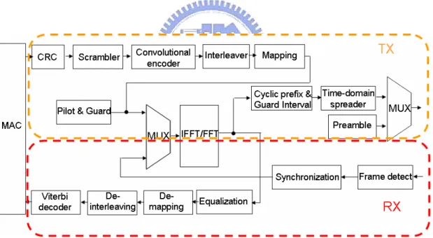
In figure 1.1, UWB physical (PHY) layer contain transmitter and receiver, but IFFT/FFT is both shared with transmitter and receiver. The IFFT/FFT in OFDM system
plays an important role for transform time domain to frequency domain or frequency domain to time domain. Because IFFT/FFT is a dual mode circuit, we can control its operation mode and use multiplexer to switch input signal. This UWB spec. [2] don ’t restrict the receive latency of PHY, but the latency of receiver is a factor of the performance in communication system. Thus, the latency of receiver must as small as possible. However, the spec. of Wireless LAN, 802.11a, which restrict PHY to only have 4 OFDM symbols latency to process receive data.[13] For local property, if we reduce the latency of each sub-block, then the system latency can be also reduced.
1.3. OFDM overview.
OFDM is a special case of multicarrier transmission, where a single data stream is transmitted over a number of lower rate subcarriers. OFDM can be seen as either a modulation technique or a multiplexing technique. One of the main reasons to use OFDM is to increase the robustness against frequency selective fading or narrowband interference. In a single carrier system, a single fade or interferer can cause the entire link to fail, but in multicarrier system, only a small percentage of subcarriers will be affected. Error correction coding can then be used to correct for the few erroneous subcarriers.[1]
“Orthogonal” means there is mathematical relationship between the frequencies of the carriers. In conventional FDM (frequency division multiplex) system, guard bands are introduced between different carriers, so it can still use conventional filters and demodulators. Unfortunately, it will result in downgrading of spectrum efficiency. It could be possible that sidebands overlapped and the signal can still avoid interference from adjacent channel. To achieve this target, the carrier must be mathematically orthogonal. In eq.(1.0)[10], is a OFDM signal described by mathematical equation, where with N subcarriers and symbol duration is T, and notice that ( )s n is the inverse Fourier Transform of the x ni( ). In figure 1.2, it illustrates spectra of eq.(1.0);
adjacent channels is all zero. 1 0 ( ) ( ) exp(2 ), for 0 ;0 , 0,1, , 1 N i i i i c A s n x n f n n N i N N i f f i N T π − = = ≤ ≤ ≤ ≤ = + = −
∑
(1.0)Figure 1.2 Spectra of an OFDM signal in frequency domain.
Further more, to eliminate the banks of subcarriers oscillators and coherent demodulators required by frequency division multiplex, digital implementation can be built by a special hardware named FFT (Fast Fourier Transform), which is an efficient implementation of DFT (Discrete Fourier Transform).
Using this method, both transmitter and receiver can be implemented using FFT techniques that reduce the number of computational load from N2 in DFT down to NlogN [9].
● OFDM is an efficient way to deal with multipath; for a given delay spread, the implementation complexity is significantly lower than that of a single carrier system with equalizer.
● In relatively slow time-varying channels, it is possible to significantly enhance the capacity by adapting the data rate per subcarriers according to the signal to noise ratio of that particular subcarriers.
● OFDM is robust against narrowband interference, because interference only affects a small percentage of subcarriers.
● OFDM make single frequency networks possible, which is especially attractive for broadcasting applications.
OFDM also has drawbacks:
● OFDM system is sensitive to frequency offset and phase noise.
●OFDM system has relatively large peak to average ratio, which tends to reduce the power efficiency of the RF amplifier. [1]
1.4. 128-point FFT for UWB spec.
In table 1.2, the 128-point IFFT/FFT period TFFT = 242.42 ns, if we using serial
one sample input and output architecture, the clock period = 242.42 ns/128 = 1.89 ns, that is, we must operate digital circuit in 528 MHz and that is very critical in 0.18 process, but we use parallel architecture and lower clock frequency to solve this problem. In figure 1.3, we use parallel 4 input samples and parallel 4 output samples and 528 MHz divide by 4 equals 132MHz, that is, we can use lower clock rate (132MHz) to fit UWB spec. by parallel FFT architecture.
Figure 1.3 Illustration of the 128-point FFT
The resolution of input bits are 5 bits and the resolution of output bits are 8 bits for system required, and we will discuss resolution in chapter 4.
1.5. Organization of this thesis.
The summary of each chapters are listed as follow:
Chapter No. & title Brief introduction
Chapter 2: Algorithm
First, we compare the computational complexity with radix-2, radix-4 and radix-8 algorithm, and then explain why we make choice of radix-8 algorithm. Finally, we introduce how to transform 128 points DFT to 128 points radix-8 FFT.
Chapter 3:
FFT module architecture
In this chapter, we introduce the architecture of 128-point FFT by bottom up sequence. The submodules are introduced first, and they include radix-8 butterfly, twiddle factor multiplier and constant multiplier. Then, we assemble all submodules to 128-point FFT and we show the timing diagram to illustrate the operational schedule. Finally, we utilize the reorder buffer to reorder output signal and we will introduce the architecture of reorder buffer and how it works. Chapter 4:
Implementation and Verification
The design and verification flow is shown first, and we discuss how to implement this design and how to verify this design. First in implementation phase, we discuss the effect of the EVM upon the word-length and how to select the word-length for system requirement. Then, we introduce an efficiency verification method and circuit performance. Finally, we show the summary of the chip implementation and compare this design with other design.
Chapter 5:
Measurement results
In this chapter, we report the FPGA synthesis reports and FPGA measurement plan and the measurement results.
Chapter 6:
Conclusion and feature works
We make a conclusion of this design and discuss what can be improving in feature works.
Chapter 2. FFT algorithm.
2.1. Discrete Fourier Transform
The N-point Discrete Fourier Transform (DFT) of a sequence x(n) is defined as
1 0 ( ) ( ) , 0,1 1 (1) N nk N n X k x n W k N − = =
∑
= −Where x(n) and X(k) are complex numbers. The twiddle factor is
2 ( ) 2 2 cos( ) sin( ) (2) nk j nk N N nk nk W e j N N π π π − = = −
Accord to eq. (1), the computational complexity is O(N2) through directly performing the required computation. It needs N2 complex multiplications and N(N-1) complex additions. If using the FFT algorithm, the computational complexity can be reduced to O(NlogrN), where r means the radix-r FFT. The radix-r FFT can be derived
from DFT by decomposing the N-point DFT into a set of recursively related r-point transform. There are two basic types of FFT algorithm, decimation in time (DIT) and decimation in frequency (DIT). The DIT algorithm is to decompose x(n) into radix-r
modules sequence, and the DIF algorithm is to decompose X(k) in the same way.
2.2. Complexity comparison
From table 2.1 [3] and table 2.2 [4], the multiplication and addition of radix-8 have the lowest complexity compared with radix-2 and radix-4. In table 2.1 radix-8 consist of constant multiplications and real multiplications. The constant multiplication can be implemented by shifters and adders whose hardware is simpler than a real multiplication. Table 2.3 [5] is the complexity equation of multiplications and additions. The radix-8 type1 algorithm is the original radix-8 FFT algorithm. In radix-8 type2 algorithm, we replaced multiplication of
1 8
W
into p additions. According to our discussion in the next section, we set the parameter p to be 3 here. But according to the large silicon area and power hungry features of complex number multiplier , we only focus on the number of real number multiplications. In figure 2.1, radix-8 type2 has the lowest computational complexity, so we choose radix-8 type2 as the building block to implement 128-points fft.
Table 2.1 Multiplicative comparison [3]
N Radix-2 Radix-4 Radix-8
Mul Mul Mul Mul Const. Mul
8 2 3 0 2 16 10 8 6 4 32 34 31 20 8 64 98 76 48 32 128 258 215 152 64 256 642 492 376 128 512 1538 1239 824 384 1024 3586 2732 2104 768 2048 8194 6487 4792 1536 4096 18434 13996 10168 4096 8192 40962 32087 23992 8192
Table 2.2 Multiplications and additions comparison [4]
Real Multiplications Real Additions
N Radix-2 Radix-4 Radix-8 Radix-2 Radix-4 Radix-8
16 24 20 152 148 32 88 408 64 264 208 204 1032 976 972 128 720 2054 256 1800 1392 5896 5488 512 4360 3204 13566 12420 1024 10248 7856 30728 28336
Table 2.3 Equation of multiplications and additions comparison [5] algorithm Real Multiplication Real Addition
Radix-2 8 2 7 log 2 3 2 N− N + N . 8 2 7 log 2 5 2 − + N N N Radix-4 log 3 3 8 9 2 N− N+ N . 3 3 log 8 25 2 N− N+ N Radix-8 type1 4 ) 3 (log 24 25 2 N− + N . 4 8 25 log 24 73 2 − + N N N Radix-8 Type2 4 8 25 log 24 21 2 N − N + N 4 8 25 log 24 73 8 2 − + + N N N p
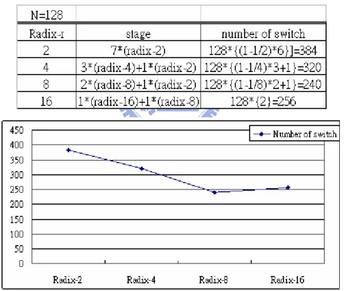
Figure 2.2 Complexity comparison of real number addition of table 2.3 In figure 2.4, it illustrate the inter connection in radix-2 FFT. We make 8 radix-2 butterfly to be an unit, then 16-point FFT needs 4 times recursive operation which needs 3 times decimation. The number of switch shows in equation (02), where N is number of points, r is radix-r, and stage is total stage. The parameter p is the number of switch in different radix. In table 2.4, we show radix-r from radix-2 to radix-16 when N is equal to 128. In figure 2.4, we show that radix-8 can provide the less number of switches. Because the number of switches is related to the complexity of the design, we chose radix-8 architecture to implement this design.
(
)
1
1 1
Number of switch N stage p
r
= × − × − +
Figure 2.3 Illustration of inter connection in FFT. Table 2.4 The number of switch.
Figure 2.4 Number of switch versus radix-r.
2.3. 128-point FFT algorithm
computing separately the even-numbered frequency samples and the odd-numbered frequency samples. The even-numbered frequency samples are
1 (2 ) 0 (2 ) ( ) 0,1,..., ( / 2) 1, N n r N n X r x n W r N − = =
∑
= − (3) This can be expressed as( / 2 1) 1 (2 ) ( 2 ) 0 / 2 (2 ) ( ) ( ) N N n r n r N N n n N X r x n W x n W − − = = =
∑
+∑
(4) With a substitution of variables in the second summation in (4), than( / 2 1) ( / 2) 1 (2 ) [ ( / 2)]2 0 0 (2 ) ( ) ( ( / 2)) N N n r n n r N N n n X r x n W x n N W − − + = = =
∑
+∑
+ (5) Finally, because of the periodicity of2rn N W 2 [r n ( / 2)]n 2rn rN 2rn N N N N W + =W W =W Since 2 / 2 N N W =W , (5) can be expressed as ( / 2 1) / 2 0 (2 ) [ ( ) ( ( / 2))] , 0,1,....( / 2) 1, N rn N n X r x n x n N W r N − = =
∑
+ + = − (6) From (6) is the (N/2)-point DFT of the (N/2)-point sequence obtained by adding the first half and the last half of the input sequence. Adding the two halves of the input sequence represents time aliasing, consistent with the fact that in computing only the even-numbered frequency samples, that are under sampling the Fourier transform of x(n). In the same way, we can get the odd-numbered frequency points, given by( / 2 1) / 2 (2 1) [ ( ) ( ( / 2))] , 0,1,....( / 2) 1, N n rn N N X r x n x n N W W r N − + =
∑
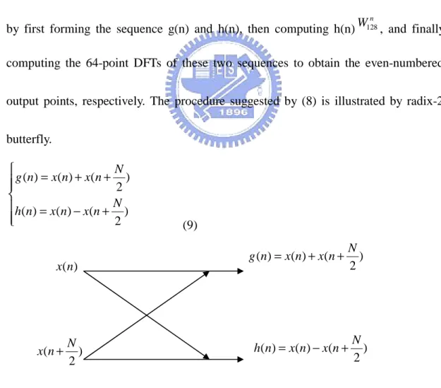
− + = −From (6) and (7) let N=128, than the even-numbered frequency samples and the odd-numbered frequency samples can be divided as eq. (8).
63 64 0 63 64 128 0 (2 ) [ ( ) ( 64)] (2 1) [ ( ) ( 64)] kn n kn n n X k x n x n W X k x n x n W W = = = + + + = − +
∑
∑
n=0,1,, 63 (8)Equation (7) is the 64-point DFT of the sequence obtained by subtracting the second half of the input sequence from the first half and multiplying the resulting sequence by
n N W
. Thus, on the basis of (6) and (7), with (9), the DFT can be computed by first forming the sequence g(n) and h(n), then computing h(n) 128
n W
, and finally computing the 64-point DFTs of these two sequences to obtain the even-numbered output points, respectively. The procedure suggested by (8) is illustrated by radix-2 butterfly. ( ) ( ) ( ) 2 ( ) ( ) ( ) 2 N g n x n x n N h n x n x n = + + = − + (9)
Figure 2.5 radix-2 butterfly
( ) ( ) ( ) 2 N g n =x n +x n+ ( ) ( ) ( ) 2 N h n =x n −x n+ ( ) 2 N x n+ ( ) x n
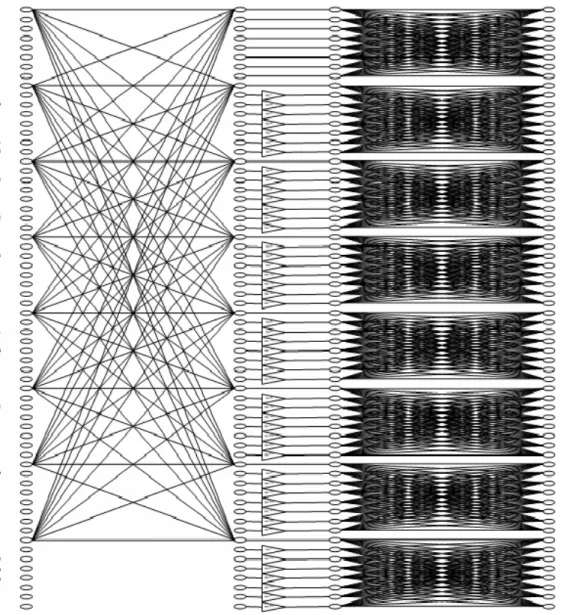
Figure 2.6 Signal flow graph of 128-point FFT algorithm.
In figure 2.5, a radix-2 butterfly operation is illustrated. In figure 2.6,the signal flow graph of DIF 128-point FFT algorithm is listed. The first stage is radix-2 butterfly with a twiddle factor multiplication, then the 64-point FFT is the second stage of 128-point FFT. The signal flow graph of DIF 64-point FFT algorithm is listed in figure 2.7, we can observe that the 64-point FFT consists of two stages radix-8
butterfly and twiddle factor multiplication. Then we will introduce the 64-point FFT algorithm at the next section.
Figure 2.7 Signal flow graph of 64-point FFT algorithm.
2.4. 64-point FFT algorithm
We use radix-8 FFT algorithm to conduct 64-point FFT algorithm. The N point DFT is rewrite at eq. (10), where N is the power of 8.
1 0 ( ) ( ) , 0,1 1, N nk N n X k x n W k N − ′ = ′ =
∑
′= − N =8 , a a∈N (10) Using the value transform, let k′ =8k+l and n= +n1 n2.0, , 1 8 8 0,1, , 7 N k Let k k l l = − ′ = + = (11) 1 2 0, , 1 1 2 8 0,1, , 7 N n Let n n n n = − = + = (12)
Replace the k′and n , the new equation will be
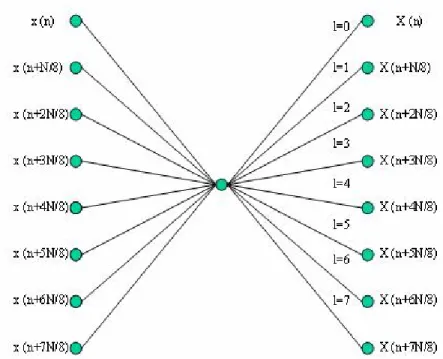
1 1 2 2 1 1 1 2 1 7 8 ( )(8 ) 8 1 2 0 0 1 7 8 1 2 8 0 0 8 8 int int 8 (8 ) ( ) 8 ( ) 8 N N n n k l N n n N ln ln kn N N n n twiddle factor po DFT N po DFT N X k l x n n W N x n n W W W − + + = = − = = − − + = + = + ⋅
∑ ∑
∑ ∑
(13)Equation (13) can be considered as two-dimensional DFT. One is 8-point DFT and the other is N/8-point DFT as shown in figure 2.8. Then, by decomposing the N/8-point DFT into the 8-point DFT recursively through a-1 times, where a is equal to log8N, we can complete the N-point radix-8 DIF FFT algorithm. In (13), the 8-point DFT which is the basic operation unit, is shown in figure 2.9. A butterfly is also an essential arithmetic component in an FFT processor. In figure 2.9, it is clearly seen that seven complex multipliers are need in a butterfly unit by direct mapping approach to implement 8-point DFT. Radix-8 FFT algorithm is seldom used in single-memory FFT architecture, because the hardware cost of its butterfly unit is too high to implement. In order to implement radix-8 FFT algorithm more efficiently, we follow the radix-23 DIF FFT algorithm.[4]
Figure 2.9 Radix-8 DIF butterfly.
To decompose butterfly of radix-8 DIF FFT algorithm into three steps and apply the radix-2 index map to the radix-8 butterfly.
From equation (13)
Let l=4l3+2l2+l1, , ,l l l3 2 1∈
{ }
0,1 And replace the value of (13) we can get3 2 1 2 3 2 1 1 1 1 2 1 2 2 1 1 1 7 8 ( 4 2 ) ( 4 2 ) 3 2 1 1 2 8 0 0 8 1 1 2 1 1 2 2 4 1 1 2 1 (8 4 2 ) ( ) 8 4 2 6 ( ) ( ) ( ) ( ) 8 8 8 5 3 ( ) ( ) ( ) 8 8 8 N l l l n l l l n kn N N n n l l l l l N X k l l l x n n W W W N N N x n x n W x n x n W W W N N N x n x n W x n − + + + + = = + + + = + ⋅ + + + + + + + + + + + + =
∑ ∑
3 2 1 2 2 1 1 3 2 1 1 1 1 8 (4 2 ) 1 2 2 4 8 0 8 point DFT ( 4 2 ) 8 point DFT 8 7 ( ) 8 N l l l l l l n l l l n kn N N twiddle factor N N x n W W W W W W − + + = + + + + ⋅ ⋅∑
………(14)Figure 2.10 Three step radix-8 DIF butterfly.
In (14), we use the radix-2 index map to divide the 8-point DFT into three steps. Figure 2.10 shows the butterfly of the three-step DIF radix-8 FFT. The twiddle factors,W and 81 W at the first step are trivial complex multiplication, because they 83
can be written as 2
(
1)
2 − j and 22
(
− −1 j)
. Thus, a complex multiplication with one of the two coefficients can be computed using additions and a real multiplication, whose hardware can be realized by four shifters and three adders. We will introduce the hardware architecture in further chapters.In eq. (14), let N=82=64 and
{ }
3 2 1
0,1, , 7, , , 0,1
(
) (
)
(
) (
)
3 2 1 2 3 2 1 1 1 1 2 1 2 2 1 1 2 2 1 7 7 ( 4 2 ) ( 4 2 ) 3 2 1 1 2 8 64 8 0 0 1 1 2 1 1 2 2 4 ( 4 1 1 2 1 1 2 2 4 8 (8 4 2 ) ( 8 ) ( ) ( 32) ( 16) ( 48) ( 8) ( 40) ( 24) ( 56) l l l n l l l n kn n n l l l l l l l l l X k l l l x n n W W W x n x n W x n x n W W W x n x n W x n x n W W W W + + + + = = + + + = + ⋅ + + + + + + + + + + + + + + =∑ ∑
3 2 1 1 3 2 1 1 1 2 ) 7 8 int 0 (4 2 ) 64 8 8 int l l po DFT n l l l n kn twiddle factor po DFT W W + + = + + ⋅ ⋅∑
………(15)In eq. (15), the 64-point FFT is based on two stage radix-8 butterfly and it needs 49 times complex multiplications exclude from W ,81 W and 83 W . The signal flow is 80
Chapter 3. FFT module architectures.
3.1. Introduction
In the domain of implementation of FFT processor, two architectures are commonly used. One is pipelined FFT, the other is memory based FFT. The pipelined architecture consumes a relatively large chip area compared with memory based architecture, because the pipelined architecture may needs more complex value multipliers and complex value adders. In chapter 1, we introduce the FFT module spec. for UWB system, the high speed, low latency and the parallel input and output is required. Because of the low latency issue, the intermediate memory access is frequently and that require one time read and two times write at one clock cycle, it is not appropriate to use RAM for intermediate memory device, so that we use register set to replace RAM, because the register set is more convenient to use for frequently and high bandwidth data access. Basically, RAM is more proper to use for input buffer and
output buffer, because of the data of input buffer and output buffer is burst and there is not any available data in most of the time period. Thus, the memory is better to design for power saving purpose for most the time the memory cell would be shut down by disabling the clock. In this chapter, we will introduce the architecture of each sub-module in detail.
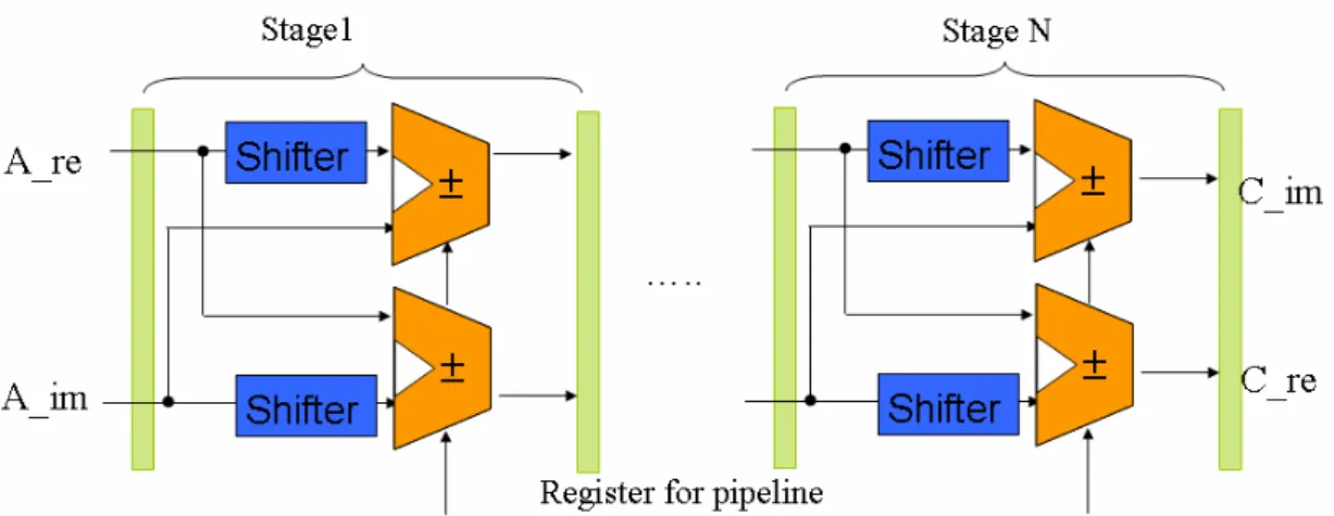
3.2. Radix-8 butterfly architecture
According figure 2.7, we redraw the figure 3.1, and we can see that radix-8 butterfly unit is composed of 12 radix-2 butterfly units and two complex multipliers
1 2 / 8 8 j W =e−π , 3 2 / 8 8 j W = je π
which we will introduce at chapter 3.4.The multiplication j is don’t need any multiplication and addition, it only need swap the real part value to image part and inversed sign of the image part.
The three step radix-8 butterfly unit is the kernel of the 128-point FFT, thus for high speed and low latency issue, we must pipeline radix-8 butterfly unit but not too much stage, because of too many stage pipeline will lead to long latency, that is not we expect. In figure 3.1 there is shown a critical path of radix-8 butterfly unit, the number is the number of addition that is used to estimate the timing delay of this critical path. It totally has 8 adders at this path and the total time delay is 9 ns without pipeline, and that is not arrival the timing specification. After 3 stage pipeline the timing arrival 3.1 ns
and latency is 3 clock cycle. Notice that the pipeline register is in the middle of complex multiplication ( 1 2 / 8 8 j W =e−π and 3 2 / 8 8 j W = je π
) that is for the architecture required and balance timing delay which will introduce later.
Figure 3.1 Architecture of Radix-8 butterfly
3.3. Twiddle factor multiplication
After Radix-8 butterfly operation is the twiddle factor multiplication, there is 7 complex multiplications (28 real multiplications) need for twiddle factor multiplication. Because of the area and latency concern about twiddle factor multiplication, we must select a compromise between area and latency is very important for 128-point FFT module design.
There are three kind of architecture to implement the twiddle factor multiplication, one is general complex multiplication the other is CORDIC-based
phased rotator [5] and the other is MAC-based complex multiplication [6]. We will
compare the each architecture as follow.
3.3.1. General complex multiplier.
In (16), expend the complex multiplier there are four real multiplications and two additions. The critical path is multiplication and we use three register to pipeline the critical path, there are two stages and have three clock cycle latency. Before pipeline the general complex multiplier can arrival 4.5ns, after pipeline it can arrival 3.15ns.
Figure 3.2 Architecture of General complex multiplication
real part image part
2 2
(Re Im ) (cos( ) sin( ) )
2 2 2 2
(Re cos( ) Im sin( )) (Re sin( ) Im cos( ))
nk nk j j N N nk nk nk nk j N N N N π π π π π π + × + = × − × + × + × (16)
3.3.2. CORDIC-Based phased rotator.
CORDIC (COrdinate Rotation DIgital Computer) It is a class of shift-add algorithms for rotating vectors in a plane. In a nutshell, the CORDIC rotator performs a rotation using a series of specific incremental rotation angles selected so that each is performed by a shift and add operation. Rotation of unit vectors provides us with a way to accurately compute trig functions, as well as a mechanism for computing the magnitude and phase angle of an input vector.
There is an example for CORDIC algorithm for phased rotate.
Iteration one that is i = 0, and we want rotate vector A to x-axis. After first one rotation the vector A0 is under x-axis and the angle a0 = tan -1(1) = 45o.
Iteration two that is i = 1, after second rotate A1 is above the x-axis and the angle a1
= tan -1(1/2) = 22.5o.
Iteration two that is i = 2, after third rotate A2 is under the x-axis and the angle a2 =
After three times rotate A2 very approach x-axis and total rotate angle a= a0-a1+a2
=35o, if there are more iteration the more approach to target rotate phase.
In figure 3.3, the CORDIC-Based phased rotator architecture contain shifter and adder in each stage, because of the requirement of the resolution, there are N times iterations needed. If let N =13, that is there are 13 iterations, and there are a very long critical path for this design, using pipeline to reduce timing delay. In this design have 13 stages and there are 14 clock cycles latency which is very long latency for phased rotator. The advantage of CORDIC-Based phase rotator is that it doesn ’t need any multiplier and after pipeline can arrival very high speed but it paid high latency for small area and high speed.
Figure 3.3 CORDIC-Based phased rotator architecture.
3.3.3. MAC-Based complex multiplier.
MAC (multiply and accumulate) is popular used for DSP processor. DSP processor often have only two real multipliers, but the complex multiplication use four multiplication that is very not efficiency for complex multiplication, and there is an algorithm to reduce the number of real multiplier. This algorithm can speed up DSP processor for complex multiplication by using MAC instruction. Besides, we can use the way to reduce real multiplication and then reduce area and power.
We can transmit (16) to (17), there need only three real multiplication and five additions. In figure 3.4, one addition is performed first and then three multiplications are performed. Finally, one addition and one subtraction complete the complex multiplication. In this complex multiplier design, the critical is two additions and one multiplier which is more timing critical than general complex multiplier. Before pipeline this design can arrival 5.5 ns, after 3 stages pipeline can arrival 3.17ns,
latency is four clock cycle.
2 2 2
Re_out Re cos( ) sin( ) (Re Im) sin( )
2 2 2
Im_out Im cos( ) sin( ) (Re Im) sin( )
nk nk nk N N N nk nk nk N N N π π π π π π = × + − + × = × − + + × (17)
Figure 3.4 MAC-Based phase rotator.
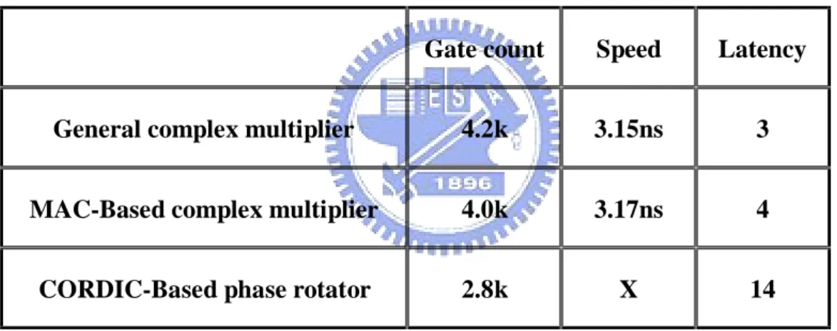
3.3.4. The comparison of twiddle factor multiplier.
There are three kind of twiddle factor multiplication, there are some trade off for those designs. In table 3.1, we can see that CORDIC-Based phased rotator have lower gate count and high speed, but latency is 14 clock cycles, that is not acceptable for
system. Then, there are general complex multiplier and MAC-based complex multiplier, the gate count and speed are nearly, but the latency is better in general complex multiplier. Finally, we decide use general complex multiplier in 128-point FFT architecture. But why the gate count of MAC-Based complex multiplier is similar to general complex multiplier, the MAC-based complex multiplier is less real multiplier than general complex multiplier. Because of the word-length of multiplier in 128-poit FFT design is only 8 bits, and multiplier can’t dominate the area.
Table 3.1 The comparison of the twiddle factor multiplication.
Gate count Speed Latency General complex multiplier 4.2k 3.15ns 3 MAC-Based complex multiplier 4.0k 3.17ns 4 CORDIC-Based phase rotator 2.8k X 14
(PS: The gate count of CORDIC-Based phase rotator is reference form [7])
Because the delay of the multiplier and adder is not balance, we can use design compiler to retiming the design. The command “set_balance_registers” is suitable for the sequential design in which register have been inserted or the design have been pipelined. This command will perform retiming and move the registers in complex multiplier to the position that will make the circuit having balance delay and minimize the cycle time. In table 3.2, general complex multiplier can speed up about 0.39ns and
MAC-based complex multiplier can speed up 0.06ns. We use the same timing constrain to synthesis those designs, but the performance of retiming in general complex multiplier is better than MAC-based complex multiplier.
Using retiming to synthesis this design can balance delay, but it has restriction that we can’t add last stage registers before synthesis. If we need last stage registers, we must add it manually later.
Table 3.2 The comparison of the twiddle factor multiplication after retiming.
Gate count Speed Latency General complex multiplier 4.0k 2.76ns 3 MAC-Based complex multiplier 3.7k 3.11ns 4
(PS : The gate count is not included input and output register)
3.4. Constant multiplier design
In radix-8 butterfly, there are complex multiplication (W81=e−2πj/ 8and
3 2 / 8 8
j
W = −je−π ) which can be implemented by constant multiplier. In (18), we can see that W83 =W81× −( j), in the other word W is 83 W phase rotate –j (figure 3.4). 81
1 4 8 3 3 4 1 8 8 2 2 2 2 2 2 ( ) 2 2 j j W e j W e j W j π π − − = = − ⋅ = = − − ⋅ = × − (18)
In (19), angle 45o phase rotate need 2
and one subtraction. Figure 3.5 is a W complex multiplier, there is a register for 81
pipeline in the middle of the constant multiplier.
(
)
(
)
(
)
constant multiplication constant multiplication
2 2 Re Im 2 2 2 Re Im 2 Im Re 2 2 j j j − ⋅ × + ⋅ = + + ⋅ − (19)
Figure 3.5 Architecture of W complex multiplier. 81
2
2 = 011101 in format 1.5 (the left of the dot is one bit, and the right of the dot are 5 bits) unsigned statement. To multiply 2
2 is only need shift and adder which shown in figure 3.7, the adder is 10 bits word-length and four shift and adder is needed. Because the W complex multiplier is under critical path, timing is the most important 81
consideration, and we reduce the word-length of adder and add pipeline register in the middle of the constant multiplier for increased speed of the circuit. In figure 3.6 we use 6 bits, 8 bits and 9 bits adder to replace 10 bits adder, because the total 16 bits are only 11 bits needed. Reducing word-length of adder not only can speed up circuit but also can reduce area, but there are some lose of resolution. Considering this trade off, the error of reducing word-length is 0.1% but it can speed up about 0.2ns, and therefore we decision to use reducing word-length adder to implement 2
2 constant multiplier.
In figure 3.7, after constant multiplier, there is a output rounding let 11 bits round to 10 bits in order to make output signal more precise. Rounding circuit only need a multiplexer and a 10 bits adder, which only need few gate count.
Figure 3.7 Architecture of constant multiplier.
3.5. 128-point FFT circuit design
The main circuit design dominates the totally performance, area, and power consumption. In order to achieve high speed and low latency, there is more parallel than the other FFT circuit design. Because of the 4 complex values input, we need 4 radix-2 butterfly units and 4 twiddle factor multiplier, shown in figure 3.8. The input buffer (B1) is 64-samples memory space and buffer input signal 16 clock cycles, then radix-2
butterfly unit and twiddle factor multiplier can operate.
Figure 3.8 128-point FFT circuit block diagram
In figure 3.9, it shows all the operation of each cycle. Notice that there are 4 twiddle factor multipliers can share with radix-2 and radix-8 butterfly, because there are no resource confliction for the twiddle factor multiplier of the radix-2 and radix-8. In 128-point FFT circuit, there is only an intermediate register set (temp register B2), which have 128-samples memory space, then, we use the in-place method to manage the read/write of the register set. Because there only an intermediate register set, the read/write of the register set needs a very high band-width for access, thus it can ’t be replaced by RAM, because RAM can only read or wire at single cycle.
of low latency. The utility of radix-8 butterfly is 50% and complex multiplier is 78.6%. In figure 3.9, there are four complex multipliers, which are working all the time, utility is 100%, another three complex multipliers are 50%,and average is 78.6% totally.
Because of resource conflict between radix-2 and radix-8 butterfly unit, radix-8 can’t share four radix-2 butterfly units for first stage. Thus, we design another four radix-2 butterfly units for first stage. Specifically, high speed design has a challenge to backend timing convergence. We consider that timing convergence problem in this design and make backend timing more easily to met, thus, we add some temp register and using synthesis constrains in transition time for more strong driving strength. By the way, those methods must cost more area but can make design more robust.
F ig u re 3 .9 T im in g d ia g ra m o f 1 2 8 -p o in t F F T
3.6. Design of reorder buffer and output buffer.
Output of DIF FFT algorithm is out of order sequence. Thus if we need in order sequence or duel FFT/IFFT mode, we need the reorder buffer to reorder the output sequence. The 128-point FFT core is 8 output samples and the output sequence shows in figure 3.10. We can see that the row of out 0 the sequence 0, 2, 4, 6, 8, 10, 12, 14, 1, 3, 5, 7, 9, 11, 13, 15 is the order of output sequence and the sequence we demanded is 0, 1, 2, 3, 4, 5, 6, 7, 8, 9, 10, 11, 12, 13, 14, 15, thus we use 8 single port RAM to construct the RAM bank and interleaving each output to different RAM on purpose. In figure 3.11, we use multiplexer to interleave the radix-8 butterfly output data and store in different address, thus the sequence 0, 1, 2, 3, 4, 5, 6, 7, 8 is in different RAM and for the same reason the sequence 9, 10, 11, 12, 13, 14, 15 is also interleaved at different RAM. By the way, reorder buffer must wait all of the radix-8 output data saving into memory, then it can start dumping output data in 16 clock cycles, that takes 19 clock cycles latency.
Figure 3.11 RAM addressing of the reorder buffer.
Figure 3.12 shows the architecture of the reorder buffer, there are two Rotate MUX for interleave data and reassembly data. The control signal sel_0 and sel_1 control the rotating order and the rw_addr controls the address of the RAM. The input and output register set make the output signal more stable.
Figure 3.12 Architecture of the reorder buffer.
Figure 3.13 shows the architecture of output buffer, the output buffer is only a parallel-to-serial which makes parallel 8 outputs to parallel 4 outputs. Every 8 points data only 4 points data are really needed save into the memory. It only needs a very simple controller to implement the output buffer circuit. The latency of the output buffer is 3 clock cycles.
Figure 3.13 Architecture of output buffer.
The different form FFT between IFFT is the sequence of the output order. The reorder buffer can pre-buffer the fist one output and let control counter to count backwards, and then we can get the IFFT sequence. Figure 3.14, using a very simple control to get IFFT sequence.
(a) Only 128-point FFT.
(b) 128-point FFT + output buffer.
(c) 128-point FFT + reorder buffer.
(d) 128-point FFT + reorder buffer + output buffer.
Table 3.3 All kinds of combination of 128-point FFT vs. Latency Output operation Latency (a) Only 128-point FFT 8 out of order output 50 clock cycles (b) 128-point FFT + output buffer 4 out of order output 54 clock cycles (c) 128-point FFT + reorder buffer 8 sequential output 70 clock cycles (d) 128-point FFT + reorder buffer +
output buffer
4 sequential output 73 clock cycles
There are many kind of combination of 128-point FFT shown in figure 3.15 and table 3.3, each combination can be selected as you needed. You can just only change parameter to define each architecture and there is a verification environment can verify each architecture.
Chapter 4. Implementation and
verification
4.1. Introduction.
In this chapter we discuss how to modeling a behavior model of the 128-point FFT and how to verify this design. Behavior model is built by MATLAB which can provide a complete mathematical and simulation environment. The design flow is illustrate in figure 4.1, and this is a kind of waterfall models which is worked well up to 100k gate count design. It is a serial flow from specification survey to post layout simulation and there integrate a verification flow to verify the design. Notice that function verification verifies the behavior module and RTL module to check if they have the same function, and it helps debugging in RTL code that saving a lot of time for debugging. After RTL code development and function verification there are two way for implement design,
one is ASIC, and the other is FPGA prototyping. FPGA prototyping is for verification design in general, because FPGA can simulate fastest than simulator and it realizes the function of the circuit by an easy way. If we want produce ASIC, we will go through synthesis and Place & Route. We synthesis the design to gate-level netlist by reasonable design constrain, and verify the timing, area and power. If it arrival out demand, we will Place & Route our design. After timing, area, power and design rule are all conformed, we can tape-out.
4.2. Behavior module design.
To develop a MATLAB behavior module to simulate a real circuit function, we need to quantize value after the mathematical operation. In figure 4.2, we illustrate all of the mathematical operation point and list the each function of the operation point. There are A, B, C, D, E five operation points in this circuit which are post-addition and post-multiplication, and column one is the word-length of the intermediate register and complex multiplier. To discuss the quantization error from the intermediate register and complex multiplier is that both of then cost most of the area and power consumption (register about 50%, complex multiplier about 20%) and they directly relate to quantization error. Let we see the column A, there are two parameter, Scale bit and Quantize bit, which means how much bits we scaled in this stage and how to quantize the word-length. In another word, if we want to present 10 bits value by using 8 bits, we must scale 2 bits and keep maximum side, thus the Scale bit set to 2. The Quantize bit (7.2) means that we quantize value by 7 bits left of the dot and 2 bits right of dot, and totally we use 9 bits to present this value, because the twiddle factor is a decimal fraction.
Figure 4.2 MATLAB simulation for word-length decision (1).
There are two methods to quantize value, one is “round”, and the other is “floor”. Notice that the SQNR by “round” is better than “floor” about 6 dB, and figure 4.3 illustrate the simulation results and the simulation condition. We use 5 bits random signal to input both ideal FFT and practical FFT, and use ideal FFT output value to get SQNR. Each SQNR was simulated about 1280000 sample points, and we simulate N from 5 bits to 10 bits to find out the quantization error vs. word-length N. Finally, we decide to use N = 8 and SQNR = 30dB for system requirement. Because the UWB system is only QPSK modulation, the SQNR = 30 dB is quite better. Figure 4.3 shows the SQNR versus word-length.
Figure 4.3 MATLAB simulations for word-length decision (2).
In figure 4.4, we simulate the quantized response of FFT and IFFT by using QPSK input value. The performance is that EVM = -17.9681 dB and SQNR = 17.9681 dB.
Figure 4.4 FFT and IFFT
4.3. Verification.
Functional verification usually cost about double time more than develop a RTL code. If there is a robust method for verify design, we can reduce a lot of time for debugging design. We have two verification phases of this design, one is debugging phase, and the other is regression phase. The debugging phase we need fully accessibility and fast turnaround time, and verilog test bench is very suit to debugging phase. Then, if most of the bug is removed, we need find out the last bug which is most hard to remove. Using regression phase to turn off most if the accessible options to increase simulation efficiency and we can use random generator to generate random pattern for input signal
and we can simulate a large number of cycles efficiently. In this design we use ADS co-simulation for regression phase debugging.
Figure 4.5 Self-check test bench
In figure 4.5, it is the structure of verilog test bench in debugging phase. There are input control and output checker. We can read input signal form Re_in.dat and
Im_in.dat which generate by MATLAB, and output checker can compare 128-point FFT output signal with MATLAB behavior module output and send correct signal. This self-check test bench can verify a lot of test patterns and we can check the output signal if the signal of correct is low, we can open waveform and debugging. This self-check test bench can save a lot of time to check output signal is correct or incorrect, efficiently. In chapter 3.6, there are many kind of combination of 128-point FFT, because the output sequence is very different, but this test bench can detect which kind of
architecture we verify and can auto reorder output data and fit verification condition. This verification environment can provide a convenient and efficiency condition to user.
Figure 4.6 ADS co-simulation.
In figure 4.6, We use ADS (Advance Design System) to run co-simulation, because ADS is GUI interface, each component can observe in working space. We compare the HDL FFT with ideal FFT and show output signal waveform in figure 4.8. Using output histogram which is illustrate in figure 4.7, to decision output bits resolution, thus we can see that the almost output range is about 7 bits, but we use 8 bits resolution to prevent overflow. After 100,000 sample points simulation, we can calculate the EVM that list in table 4.1, the EVM = -30dB.
Figure 4.7 Output histogram.
Table 4.1 ADS co-simulation for EVM (dB)
There are some important signal processes in this circuit design; the anti-saturate circuit can prevent large distortion after round or truncation. Because we present values by two’s complement, we want round value 127.5 to 128 in 8 bits resolution is impossible because there can’t have value 128, but rounding will round value 127.5 to -128 and it will occur a large error. Figure 4.9 shows the anti-saturate operation; we saturate the output value with 32, but real output value is about 35. Even a large error occurs but if there isn’t anti-saturate circuit, a very large error will occur. Figure 4.10 shows the saturated output error vector; it is large but we can tolerate.
Figure 4.9 Saturated output operation.
Figure 4.10 Saturated output error vector.
4.4. Timing verification.
In table 4.2, synthesis report for each combination, there are two kind of report, one is with RAM, and the other is RAM free. We replace RAM by the register set to synthesis because we can’t calculate the gate count of RAM (RAM is likely an analog
device), so the total report of the gate count is without including RAM. In this design that can operate up to 300 MHz in synthesis phase, but this don’t include wire load and interconnect capacitance that we will concern in backend flow.
Table 4.2 Synthesis reports Gate count Speed RAM
128-point FFT 87K 3.34ns RA1SH16x40 x1 128-point FFT +output_buffer 90K 3.34ns RA1SH16x40 x1 RA1SH16x64 x1 128-point FFT +reorder_buffer +output_buffer 97K 3.34ns RA1SH16x40 x1 RA1SH16x64 x1 RA1SH16x16 x8 128-point FFT 89K 3.37ns X 128-point FFT +output_buffer 100K 3.37ns X 128-point FFT +reorder_buffer +output_buffer 130K 3.37ns X
Synthesis tools: Synopsys design compiler V-2003.12-SP1 Library: UMC018 generic slow (125oC 1.68V) library
4.5. Chip implementation.
Figure 4.11 is the new version of 128-point FFT layout view, there are summary of this chip as follow.
P&R tool : Astor
Timing sign-off tool : Prime time Power analyze tool : Prime power
Core size 1564.86 x 1564.64 um2 Die size 2554.66 x 2555.125 um2 Timing 5ns = 200 MHz
Power 127 mW @ 132 MHz Table 4.3 The chip summery.
4.6. FPGA prototyping.
We use FPGA to implement design and the synthesis report shows in table 4.4, the report of the FPGA gate count is very different from the report of the ASIC gate count, which is only for reference. Because this FPGA is 0.25 technology and the characteristic of FPGA is for verification, the timing is not very important by FPGA prototyping.
Table 4.4 Xilinx FPGA synthesis report. Target Device xcv2000e-bg560-6
Slices 7784
Slices Flip Flops 5088 Gate count 165,537
Post – Map timing 16.578ns (10.215ns logic, 6.363ns route) = 60.32 MHz
Post- Place & Route timing 25.16ns (9.936ns logic, 14.974ns route) = 39.74 MHz
4.7. Compared with other design.
Table 4.5 Comparison of 128-point FFT
This design Parallel FFT with CORDIC [7]
Synthesis speed & synthesis library
3.34ns with UMC018 slow library
7.57ns with TSMC025 Synthesis gate count 97K 87K(without
reorder buffer) 53K Latency 50+19+3+1=73 clock cycle 54 clock cycle (without reorder buffer) 99 clock cycle Synthesis Power 97 mW 109 mW P&R speed 5 ns NA
P&R core area 1564.86 x 1564.64 um2 NA P&R power 127 mW (without RAM) NA
IFFT/FFT dual core Yes No
resolution Word length = 8 bits SQNR=30dB
Word length = 8 bits Architecture Radix-8 Radix-4
CORDIC Table 4.6 Comparisons. Word length Tech. Core Area Power Operation speed Max Speed Latency Proposed (128 points) 8 bits UMC CMOS 0.18μm 2.4 mm2 127 mW (without RAM) 132 MHz 200 Mhz 73 clock cycle [11] (64 points) 16 bits IHP BICMOS 0.25μm 6.8 mm2 41 mW 20 Mhz 38 Mhz 77 clock cycle [12] (128 points) 12 bits CMOS 0.6μm 10 mm2 400 mW 50 Mhz 50 Mhz 150 clock cycle
Chapter 5. Measurement results
5.1. FPGA measurement plan.
We utilize FPGA phototype to verify this design. In figure 5.1, we add two circuit for verification, one is S-to-P (serial to parallel), and the other is P-to-S (parallel to serial). Because the limit of the input/output pin of the instrument, we translate parallel input/output to serial input/output for convenient measurement. The FPGA synthesis tool is Xilinx ISE 6.2 and synthesis report shows in table 5.1. This synthesis report is different from table 4.4; the table 5.1 includes S-to-P and P-to-S but table 4.4 only have 128-point FFT core. So that it contain two clock domains, one is clk that clock is for S-to-P and P-to-S, and the other is clk4 that clock is for 128-point FFT core. Figure 5.2 shows the measurement environments.
Figure 5.1 FPGA measurement plan
Table 5.1 Xilinx FPGA synthesis report for measurement. Target Device xcv2000e-bg560-6
Slices 7827
Slices Flip Flops 5238 Gate count 167,037
clk 4.359ns (2.945ns logic, 1.414ns route) = 229 MHz
Post – Map timing
clk4 (core clock) 16.578ns (10.215ns logic, 6.363ns route) = 60.32 MHz clk 7.875ns (2.945ns logic, 4.930ns route) = 132 MHz
Post- Place & Route timing
clk4 (core clock)
23.848ns (9.715ns logic, 14.133ns route) = 41.93 MHz
5.2. FPGA measurement results.
We use pattern generator to generate input pattern, figure 5.3 shows the input sin wave in logic analyzer at clock period = 10 ns (clk= 10 ns clk4 = 40 ns) and figure 5.4 shows the output results. But why we use sin wave for input signal? The answer is that we want to verify the output saturate operation, because the sin wave input will produce an impulse in FFT output and this impulse will saturate output.
Figure 5.3 FPGA input signal (view from Logic Analyzer).
Figure 5.4 FPGA output signal (view from Logic Analyzer).
After using logic analyzer to dump output signal to a file, we want to verify this output signal is correct or not. Using MATLAB to read data which dump by logic
analyzer we compare FPGA output with ideal 128-point FFT output. Figure 5.5 shows the results, and the function of the 128-point FFT is work.
![Table 1.2 Timing-related parameters. [2]](https://thumb-ap.123doks.com/thumbv2/9libinfo/8736875.203347/12.892.135.761.321.705/table-timing-related-parameters.webp)
![Table 2.1 Multiplicative comparison [3]](https://thumb-ap.123doks.com/thumbv2/9libinfo/8736875.203347/21.892.242.651.201.693/table-multiplicative-comparison.webp)
![Table 2.3 Equation of multiplications and additions comparison [5]](https://thumb-ap.123doks.com/thumbv2/9libinfo/8736875.203347/22.892.148.754.144.1024/table-equation-multiplications-additions-comparison.webp)