Electroluminescence from monolayer ZnO nanoparticles using
dry coating technique
Chun-Yu Lee,1Yuen-Yung Hui,1Wei-Fang Su,2and Ching-Fuh Lin1,3,a兲 1
Graduate Institute of Photonics and Optoelectronics, National Taiwan University, Taipei 10617, Taiwan 2Graduate Institute of Materials Science and Engineering and Department of Materials Science and Engineering, National Taiwan University, Taipei 10617, Taiwan
3Graduate Institute of Electronics Engineering and Department of Electrical Engineering, National Taiwan University, Taipei 10617, Taiwan
共Received 21 March 2008; accepted 6 June 2008; published online 1 July 2008兲
We report ultraviolet electroluminescence from ZnO nanoparticle-based devices prepared by the dry-coating technique. With dry-coating process, the structure of the ZnO nanoparticle monolayer 共90 nm兲 in the device can be easily achieved. The method reduces the density of pinhole defects in the ZnO nanoparticles. The confirmation for dry coating is investigated using field-emission scanning electron microscopy. The devices show the ZnO band-gap emission peak at 380 nm and the background emission from the interface between the host matrix and Aluminum tris-8-hydroxyquinoline. The origins of the ZnO band-gap emission and background emission are also discussed. © 2008 American Institute of Physics.关DOI:10.1063/1.2952283兴
Zinc oxide 共ZnO兲 is a promising semiconductor with a wide direct band-gap of 3.37 eV. Due to its large exciton binding energy共60 meV兲, the excitons in ZnO are thermally stable at room temperature. It has been regarded as one of the most promising candidates for the next generation of ultra-violet共UV兲-blue light-emitting diodes 共LEDs兲 and lasing de-vices operating at high temperatures and in harsh environ-ments. A few studies have been reported on the development of heterojunction LEDs using ZnO thin film,1–7 ZnO nanowires,8–14or ZnO nanoparticles.15,16In the past, we have reported the use of phase-segregation technique to fabricate the ZnO nanoparticle electroluminescent 共EL兲 devices.16 With phase segregation, the ZnO nanoparticles and organic material will form a heterostructure. This method can im-prove the probability that electrons and holes recombine in the ZnO nanoparticles to enhance the band-gap emission. However, it is not easy to achieve the phase segregation. In addition, the thickness of ZnO nanoparticles is very difficult to control. Here we report an approach, dry-coating method, to fabricate ZnO EL devices with heterostructure. The ZnO monolayer can be easily achieved by dry coating. Unlike the phase segregation, which requires a particular type of hole-transporting material and special conditions of solvents, the dry-coating method is applicable to several hole-transporting materials. The method has the prominent advantage of mak-ing the cost of ZnO EL devices less expensive.
In this work, we prepare three types of ZnO EL devices formed with a host polymer, ZnO nanoparticle monolayer, and an electron transporting layer. The following host matrix materials dissolving in chloroform with different concentra-tion are chosen respectively: 0.7 wt % poly共fluorene兲 共PF兲, 1 wt % poly共N-vinylcarbazole兲 共PVK兲, and 0.7 wt % poly共3-hexylthiophene兲 共P3HT兲. For the electron transporting layer we employed small-molecular aluminum tris-8-hydroxyquinoline 共Alq3兲. The ZnO nanoparticles were pur-chased from Aldrich. The diameter of the ZnO nanoparticles
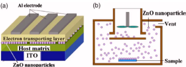
is 90 nm. The procedure of device fabrication is as follows. First, we clean the indium tin oxide 共ITO兲 glass by de-ionized water, acetone, and isopropyl alcohol sequentially. Then the host matrixes are spin coated on ITO glass respec-tively. In order to get the optimized film-forming property, the different host matrixes have the different thickness by different spin-coating condition共PF: 200 nm, PVK: 900 nm, and P3HT: 110 nm兲. These samples are baked at 170 °C 共device I兲, 170 °C 共device II兲, and 120 °C 共device III兲 for 2 h individually. Then we deposit the ZnO nanoparticles on each host matrix by dry coating under the temperature of 85 ° C and subsequently annealed at 120 ° C for 2 h to im-prove the contact between the ZnO nanoparticles and the host matrix. Then the solution containing the 0.5 wt % Alq3 is spun on top of the ZnO nanoparticles and subsequently annealed at 60 ° C for 2 h to remove the solvent. Afterward, 2000 Å of aluminum 共Al兲 was deposited onto the electron transporting layer using thermal evaporation under a vacuum of 3⫻10−6torr. The emitting area is 0.7⫻0.3 cm2. The de-vice structure is ITO/host matrix/ZnO nanoparticles 共monolayer兲/Alq3/Al. The schematic of the device structure is shown in Fig.1共a兲.
In the past, the organic/inorganic EL devices are mainly fabricated by spin coating.14–16 The organic/inorganic composites are formed through dispersion of inorganic nano-particles within the polymer matrix.14–16 However, the hy-brid structure is a disadvantage for carrier recombination in nanoparticles due to the high density of pinhole defects
a兲Author to whom correspondence should be addressed. Tel.: 886-2-3366
3540. FAX: 886-2-2364 2603. Electronic mail: [email protected].
FIG. 1.共Color online兲 共a兲 Cross-sectional schematic of the ZnO EL device structure.共b兲 The schematic of the dry-coating machine.
APPLIED PHYSICS LETTERS 92, 261107共2008兲
0003-6951/2008/92共26兲/261107/3/$23.00 92, 261107-1 © 2008 American Institute of Physics
in nanoparticle aggregations. The pinhole defects could cause the excitons quenching and inconsistent device performance.15,16 In order to reduce the density of pinhole defects in ZnO nanoparticles, the development of the ZnO nanoparticle monolayer layer is required.
In this study we show that with the dry-coating tech-nique, ZnO nanoparticle monolayer can be achieved in ZnO nanoparticle/polymer composite. During the dry-coating pro-cess, the ZnO nanoparticles are adsorbed on the host matrix using ZnO nanoparticle smog during dry-coating process. The ZnO nanoparticle smog is making by homemade nanosmog-making machine, as shown schematically in Fig.
1共b兲. In the dry-coating procedure, the ZnO nanoparticles may aggregate due to the electrostatic force. However, the latter process using the Alq3 solution could cause the aggre-gated ZnO nanoparticles without direct contact with the host matrix to disintegrate. The remained ZnO nanoparticles ad-sorbed on the surface of the hole-transporting layer then form a nanoparticle monolayer 共90 nm兲, which is sand-wiched between the organic thin films. The bottom host ma-trix adsorbs the ZnO nanoparticles. The top electron trans-porting layer, Alq3, serves three important functions. First, electron injection is enhanced. Second, quenching of radia-tive recombination near the metal interface is avoided. Third, the ZnO nanoparticle monolayer is achieved.
The field-emission scanning electron microscopy 共FESEM兲 is utilized to examine the formation of the ZnO nanoparticle monolayer. With the process using the Alq3 so-lution, the ZnO nanoparticles will form the ZnO nanoparticle monolayer on the host matrix共P3HT兲. Figure2共a兲shows the depth profile of ZnO nanoparticle distribution after an Alq3 thin layer was spun on the ZnO nanoparticles. It can be seen that the ZnO nanoparticle layer with a thickness of 90 nm is sandwiched between the P3HT and the Alq3 thin films. Moreover the Alq3 overlayer can be planar with a smooth surface, as shown in Fig.2共b兲. In contrast, without the pro-cess using the Alq3 solution, the ZnO nanoparticles will not form the ZnO nanoparticle monolayer. It can be seen from the depth profile in Fig. 2共c兲 that several layers 共approxi-mately microns兲 of the ZnO nanoparticle are covered on the host matrix共P3HT兲. For the surface morphology in Fig.2共d兲,
a surface coverage of the ZnO nanoparticle of 89% is ob-tained. It indicates that the ZnO nanoparticle adsorption on the host matrix during dry-coating process is easy.
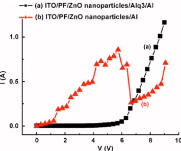
The I-V curves in dc bias mode of the ZnO EL devices with and without Alq3 are shown in Fig.3, using Al as the cathode material. For the device with Alq3, the I-V curve 共curve a兲 shows stable and good linear I-V dependence under forward bias. The turn-on voltage is about 6 V. However, for the device without Alq3, the corresponding I-V curve共curve b兲 is unstable, indicating that the pinhole defects lead to un-stable current injection in the ZnO nanoparticles and poor device performance. Hence the electron transporting layer plays a very important role for device performance.
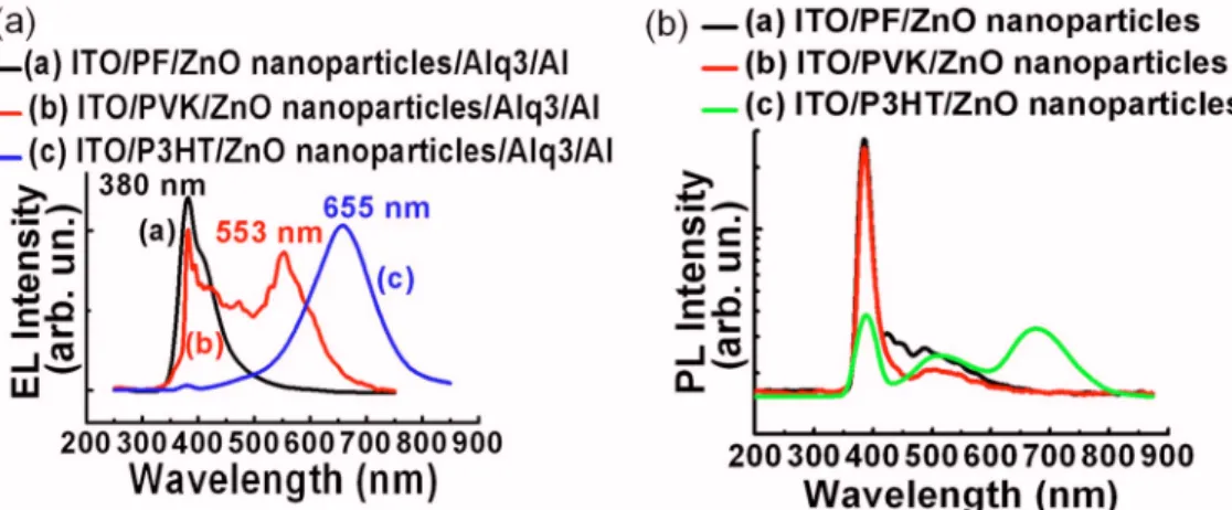
The EL characteristics of the ZnO nanoparticle devices are also measured. Figure4共a兲shows the EL spectra of the three kinds of the ZnO nanoparticle devices under forward bias of 9 V. For the device with PF共device I, curve a兲, the EL spectrum shows a strong ZnO band-gap emission peak at 380 nm with the broad background emission from PF. The full width at half maximum of the spectrum is 100 nm. For the device with PVK共device II, curve b兲, it shows a broad-band spectrum from 380 to 700 nm, which are the character-istics of the emissions of the ZnO nanoparticles 共380 nm兲 and PVK共553 nm兲. The emissions indicate that the radiative recombination occurs in the ZnO nanoparticles and at the host matrix/Alq3 interface. For the device with P3HT 共de-vice III, curve c兲 at the same forward bias of 9 V, it also has a peak around 380 nm contributed from ZnO. However the EL spectrum showed another strong background emission peak from P3HT at 655 nm. The suppression of the ZnO band-gap emission and the enhancement of the broad back-ground emission from host matrix imply that the energy transfer from higher-energy emission material共ZnO nanopar-ticle: 3.3 eV兲 to lower-energy emission material 共P3HT: 1.6 eV兲 is very strong. Exciton generation on the host matrix occurs via two parallel processes: direct charge injection and exciton transfer from the higher-energy ZnO. For direct charge injection, carriers may be trapped at the host material owing to the voids in the single ZnO monolayer. Alterna-tively, excitons can be formed in the ZnO nanoparticles that are near the host matrix. These excitons can then undergo Förster energy transfer to the lower-energy host material FIG. 2. 共Color online兲 FESEM images of the ZnO nanoparticle layer 共a兲
after spin Alq3共cross-sectional view兲; 共b兲 after spin Alq3 共top view兲; 共c兲 before spin Alq3共cross-sectional view兲; and 共d兲 before spin Alq3 共top view兲.
FIG. 3.共Color online兲 The room temperature I-V curves in the dc bias mode of the ZnO nanoparticle/PF EL device共a兲 with Alq3; 共b兲 without Alq3.
261107-2 Lee et al. Appl. Phys. Lett. 92, 261107共2008兲
sites, where they recombine radiatively. Thus the enhance-ment of the ZnO band-gap emission could be addressed by 共1兲 improving the coverage of the ZnO monolayer on the host matrix to increase current injection into the ZnO nano-particles and 共2兲 using the higher-energy host material to avoid the energy transfer between the ZnO nanoparticles and the host material. In addition, the usual emission around 560 nm from the O-vacancy defects of ZnO is not observed. Also, although Alq3 is used in our devices, its emission around 532 nm does not appear.
To investigate the origin of the EL band, photolumines-cence共PL兲 spectra of host matrix/ ZnO nanoparticles excited using the 266 nm of a Nd-YAG共yttrium aluminum garnet兲 laser are also measured at room temperature and shown in Fig.4共b兲. For the device with the higher-energy host matrix 共PF/PVK兲, the PL spectra show the emission band in the ZnO band-gap emission 共380 nm兲 with a weak emission band from the host matrix. For the device with the lower-energy host matrix 共P3HT兲, the PL spectrum shows the de-creased ZnO band-gap emission and the strong host matrix emission, which is due to the Förster energy transfer from the higher-energy ZnO to the lower-energy host matrix. Thus, the ZnO EL device with the lower-energy host matrix causes the poor ZnO band-gap emission.
In conclusion, we report the use of dry-coating technique to fabricate the ZnO nanoparticle EL devices. The dry coat-ing makes the structure of the ZnO nanoparticle monolayer in the device possibly employed. The ZnO monolayer 共90 nm兲 structure can reduce the probability that electrons and holes recombine in the pinhole defects. The FESEM analysis reveals that the ZnO monolayer is sandwiched be-tween the organic transporting materials. Here we demon-strate three types of the ZnO nanoparticle EL devices. These devices show a ZnO band-gap emission peak at 380 nm and
the background emission from the host matrix. The emis-sions occur via two parallel processes of exciton generation: direct carrier injection and exciton energy transfer. The dry-coating technique revealed in this work shows a convenient way to fabricate ZnO EL devices with very low cost.
This work was supported by the National Science Coun-cil, Taiwan, Republic of China, with Grant Nos. NSC96-2221-E-002-277-MY3 and NSC96-2218-E-002-025.
1C. P. Chen, M. Y. Ke, C. C. Liu, Y. J. Chang, F. H. Yang, and J. J. Huang, Appl. Phys. Lett. 91, 091107共2007兲.
2G. Du, Y. Cui, X. Xiaochuan, X. Li, H. Zhu, B. Zhang, Y. Zhang, and Y.
Ma,Appl. Phys. Lett. 90, 243504共2007兲.
3A. Nakamura, T. Ohashi, K. Yamamoto, J. Ishihara, T. Aoki, J. Temmyo,
and H. Gotoh,Appl. Phys. Lett. 90, 093512共2007兲.
4S. A. M. Lima, M. R. Davolos, W. G. Quirino, C. Legnani, and M.
Cre-mona,Appl. Phys. Lett. 90, 023503共2007兲.
5J. L. Zhao, X. W. Sun, S. T. Tan, G. Q. Lo, D. L. Kwong, and Z. H. Cen, Appl. Phys. Lett. 91, 263501共2007兲.
6P. Chen, X. Ma, and D. Yang,Appl. Phys. Lett. 89, 111112共2006兲. 7D. J. Rogers, F. Hosseini Teherani, A. Yasan, K. Minder, P. Kung, and M.
Razeghi,Appl. Phys. Lett. 88, 141918共2006兲.
8W. I. Park and G. C. Yi,Adv. Mater.共Weinheim, Ger.兲 16, 87共2004兲. 9R. Könenkamp, R. C. Word, and M. Godinez,Nano Lett. 5, 2005共2005兲. 10J. Bao, M. Zimmler, F. Capasso, X. Wang, and Z. F. Ren, Nano Lett. 6,
1719共2006兲.
11S. J. An and G. C. Yi,Appl. Phys. Lett. 91, 123109共2007兲.
12C. Y. Chang, F. C. Tsao, C. J. Pan, G. C. Chi, H. T. Wang, J. J. Chen, F.
Ren, D. P. Norton, S. J. Pearton, K. H. Chen, and L. C. Chen,Appl. Phys. Lett. 88, 173503共2006兲.
13R. Konenkamp, Robert C. Word, and C. Schlegel,Appl. Phys. Lett. 85,
6004共2004兲.
14M. C. Jeong, B. Y. Oh, M. H. Ham, and J. M. Myoung,Appl. Phys. Lett.
88, 202105共2006兲.
15E. S. P. Leong and S. F. Yu, Adv. Mater. 共Weinheim, Ger.兲 18, 1685
共2006兲.
16C. Y. Lee, Y. T. Huang, W. F. Su, and C. F. Lin,Appl. Phys. Lett. 89,
231116共2006兲.
FIG. 4.共Color online兲 共a兲 Comparison of EL spectra of ZnO-based nanocomposties with different host matrixes. 共b兲 Room temperature PL spectra of three host matrixes共PF, PVK, and P3HT兲 with ZnO nanoparticles 共The intensities are plotted in logarithmic scale, in order to distinguish from the different intensities of the different samples clearly兲.
261107-3 Lee et al. Appl. Phys. Lett. 92, 261107共2008兲