國 立 交 通 大 學
顯 示 科 技 研 究 所
碩士論文
高頻譜效率之正交分頻多工技術
應用於倍頻光載微波信號系統
High Spectral Efficiency OFDM Generation
for Radio-over-fiber System with Frequency
Multiplication
研
究
生 : 江 文 智
指 導 教 授 : 陳 智 弘 老師
高頻譜效率之正交分頻多工技術
應用於倍頻光載微波信號系統
High Spectral Efficiency OFDM Generation
for Radio-over-fiber System with Frequency
Multiplication
研 究 生 :江文智 Student : Wen-Jr Jiang
指導教授 :陳智弘 博士 Advisor : Dr. Jyehong Chen
國 立 交 通 大 學
顯 示 科 技 研 究 所
碩 士 論 文
A Thesis
Submitted in Partial Fulfillment of the Requirements For the Degree of Master in
Department of Photonics and Display Institute College of Electrical Engineering and Computer Science
National Chiao-Tung University HsinChu, Taiwan 300, R.O.C.
Acknowledgements 在碩士班這兩年,首先感謝我的指導老師 陳智弘教授,提供良 好的實驗環境以及無私的指導與照顧,讓我在碩士生涯中成長許多。 實驗方面特別感謝林俊廷學長教導我許多實驗方法以及報告技巧,無 私的指教與修正了我許多理論觀念,如果沒有學長如此的耐心指導下 這篇論文無法如此順利的誕生,另外感謝施伯宗學長,彭鵬群學長提 供我許多實驗技巧,還有林玉明學長,在程式方面提供了我不少的幫 助。 接下來要謝謝實驗室的伙伴:非常感謝大鵬在實驗上的幫忙,感 謝已經畢業的曹正、小彭及教練學長們,讓我碩一生活不孤單,另外 謝謝小高、小 P 及易成陪伴我一起走過碩士班的生涯,還有學弟妹們, 而咨、士愷、昱宏、漢昇、星宇在我實驗忙碌時,熱心地幫忙處理瑣 事。 還有謝謝高中到研究所的同學朋友們,你們的加油與鼓勵喔。 最後要感謝我的家人,媽媽的支持賦予我神奇的力量,爸爸的擔 心,親戚的加油及照顧,因為你們我才能勇敢地克服困難,完成碩士 學位。 帶著歡笑與淚水編織而成的回憶,邁向下個新奇的旅程,再會了交 大。 江文智 于 風城 交大 民國九十七年六月
高頻譜效率之正交分頻多工技術
應用於倍頻光纖擷取系統
研 究 生: 江文智 指導教授: 陳智弘 博士
國立交通大學 電機資訊學院
顯示科技研究所
摘要 本篇論文提出一種新型的光調變技術,此種調變技術可以傳輸向 量訊號並具有倍頻效果。利用單一驅動的光調變器產生載子抑制調變, 驅動信號為10-GHz 的正弦信號組合在 5-GHz 的 1.25-Gb/s 的開關鍵 控,二相移相鍵控或四相移相鍵控信號,在光偵測器接受後,產生在 15-GHz 的倍頻微波信號。傳輸五十公里的單一模態光纖後,三種不 同的信號靈敏度下降小於0.2dB,四相移相鍵控較開關鍵控擁有兩倍 的頻譜效益而且將近提升2dB 的靈敏度。並且我們展示正交分頻多 工調變的下傳信號與波段再利用得到的上傳信號,系統的上傳信號為 5-Gb/s 的 16QAM 正交分頻多工調變信號與透過反射半導體光放大器 傳送1.25-Gb/s 的 OOK 下傳信號。High Spectrum Efficiency OFDM Generation for
Radio-over-fiber System with Frequency Multiplication
Student: Wen-Jr Jiang Advisor: Dr. Jyehong Chen
Department of Photonics and Display Institute,
National Chiao Tung University
ABSTRACT
This investigation presents a novel modulation approach for generating optical vector signals using frequency multiplication based on double sideband with carrier suppression. A single-electrode Mach-Zehnder modulator (MZM) is biased at null point with a driving signal consists of a 10-GHz sinusoidal signal and a 5-GHz sinusoidal signal modulated with 1.25-Gb/s on-off keying (OOK), 1.25-Gb/s binary phase shift keying (BPSK) data or 625-MSym/s quadruple phase shift keying (QPSK) data. After square-law photo detection, 1.25-Gb/s RF signal at a sum frequency of 15 GHz is generated. After transmission over 50-km single mode fiber (SMF), the power penalty of all three modulation formats is under 0.2 dB. QPSK format has twice the spectral efficiency and approximately 2 dB better receiving sensitivity than OOK format. And we also demonstrate OFDM signal with wavelength reuse for uplink signal. The 5-Gb/s 16QAM OFDM signal for ROF downstream link and 1.25-Gb/s OOK signal via RSOA for upstream link are demonstrated.
CONTENTS
Acknowledgements...i
Chinese Abstract... ii
English Abstract... iii
Contents... iv
List of Figures...vi
List of Tables...x
Chapter 1 Introduction ... 1
1.1 Review of Radio-over-fiber system ... 1
1.2 Basic modulation schemes ... 2
1.3 Motivation ... 4
Chapter 2 The Concept of New Optical Modulation System ... 5
2.1 Preface ... 5
2.2 Mach-Zehnder Modulator (MZM) ... 5
2.3 Single-drive Mach-Zehnder modulator ... 6
2.4 The architecture of ROF system ... 6
2.4.1 Optical transmitter ... 6
2.4.2 Optical signal generations based on LiNbO3 MZM ... 7
2.4.3 Communication channel ... 9
2.4.4 Demodulation of optical millimeter-wave signal ... 10
2.5 The new proposed model of optical modulation system ... 12
Chapter 3 The theoretical calculations of Proposed system ... 15
3.1 Introduce MZM ... 15
3.2 Theoretical calculation of single drive MZM ... 18
3.2.1 Bias at maximum transmission point ... 18
3.2.3 Bias at null point ... 20
3.3 Theoretical calculations and simulation results ... 20
3.3.1 The generated optical signal ... 20
3.3.2 The generated electrical signal ... 26
3.3.3 Consider dispersion effect ... 30
3.4 The generated optical signal using optical filtering ... 35
3.4.1 Analysis of the generated signal ... 35
3.4.2 The effects of fiber dispersion ... 40
3.5 The optimal optical power ratio condition ... 45
3.5.1 Signal without optical filtering... 45
3.5.2 When the LSB2 or LSB1 is filter out ... 48
Chapter 4 Experimental Demonstration of Proposed System ... 50
4.1 preface ... 50
4.2 Experimental results for optical signal without optical filtering .. 51
4.2.1 Experiment setup ... 51
4.3.2 Optimal condition for RF signal ... 53
4.3.3 Transmission results ... 60
4.4 Experimental setup for optical signal with optical filtering ... 62
4.4.1 Experiment setup ... 62
4.4.2 RF signals at sum frequency ... 63
4.4.4 RF signal at different modulation index ... 69
Chapter 5 Experimental Demonstration of OFDM Signal Generation .. 73
5.1 Introduction OFDM generation system ... 73
5.2 Experimental Concept and Setup ... 74
LIST OF FIGURES
Figure 1-1 Basic structure of microwave/millimeter-wave wireless system. ... 2
Figure 1-2 the Radio-over fiber system. ... 2
Figure 2-1 (a) and (b) are two schemes of transmitter and (c) is duty cycle of subcarrier biased at different points in the transfer function. (LO: local oscillator) ... 7
Figure 2-2 Optical microwave/mm-wave modulation scheme by using MZM. ... 9
Figure 2-3 The model of communication channel in a RoF system. ... 10
Figure 2-4 The model of receiver in a ROF system. ... 11
Figure 2-5 The model of ROF system. ... 11
Figure 2-6 Concept of the proposed system. (LD: laser diode, MZM: Mach-Zehnder modulator, SMF: single mode fiber, C: circulator, FBG: fiber bragg grating, RSOA: reflective semiconductor optical amplifier) ... 13
Figure 2-7 Simulation of RF performance fading versus SMF transmission length. .. 14
Figure 3-1 The principle diagram of the optical mm-wave generation using balanced MZM... 18
Figure 3-2 The different order of Bessel functions vs. m. ... 19
Figure 3-3 The different order of Bessel functions vs. m. ... 23
Figure 3-4 Illustration of the optical spectrum at the output of the MZM. ( 2 6 1) ... 25
Figure 3-5 Illustration of the optical spectrum at the output of the MZM. ... 26
Figure 3‐6 Illustration of the electrical spectrum of generated BTB mm‐wave signals using MZM after square‐law PD detection. ( 2 6 1) ... 28
Figure 3-7 The RF signal power ratio (RFPR, 11, ) as a function of MI. ... 29 Figure 3-8 shows the numerical and theoretical solution for RF signal fading issue
after transmission. ... 34
Figure 3-9 RF power vs. 1. ... 34
Figure 3-10 shows the optical spectrum when the LSB1 is filter out. ... 35
Figure 3-11 shows the optical spectrum when the LSB2 is filter out. ... 35
Figure 3-12 Illustration of the electrical spectrum of generated BTB mm-wave signals when the LSB1 is filter out. ( 2 6 1) ... 39
Figure 3-13 Illustration of the electrical spectrum of generated BTB mm-wave signals when the LSB2 is filter out. ( 2 6 1) ... 39
Figure 3-14 shows the RF signal power vs. transmission length when the LSB1 is filter out. ... 44
Figure 3-15 shows the RF signal power vs. transmission length when the LSB2 is filter out. ... 44
Figure 3-16 shows optical spectrum without fiber grating filter out. ... 47
Figure 3-17 the e-filed power for BPSK signal between zero and one. ... 47
Figure 3-18 the e-filed power for OOK signal between zero and one. ... 47
Figure 3-19 shows optical spectrum when the LSB2 is filter out. ... 49
Figure 3-20 shows optical spectrum when the LSB1 is filter out. ... 49
Figure 4-1 the optical spectrum for the fiber Bragg grating reflection and transmission. ... 50
Figure 4-2 shows the experimental setup to receive sum frequency. ... 53
Figure 4-3 shows the optical spectrum for BPSK. ... 54
Figure 4-4 shows the optical spectrum for OOK. ... 55
Figure 4-5 the BER curves for BPSK at 5GHz. ... 56
Figure 4-6 the BER curves for OOK at 5GHz. ... 56
Figure 4-9 the BER curves for OOK at 15GHz ... 58
Figure 4-10 the eye diagrams for BPSK at 15GHz... 58
Figure 4-11 measured receiving sensitivity at BER=10-9 of OOK and BPSK signals versus SOPR. ... 59
Figure 4-12 the simulation result of MER and Q factor for BPSK, OOK and QPSK. 59 Figure 4-13 the BER curves of OOK, BPSK and QPSK signals. ... 60
Figure 4-14 the eye diagrams for BPSK signal w/o filtering... 60
Figure 4-15 the eye diagrams for OOK signal w/o filtering. ... 61
Figure 4-16 the constellations and I/Q eye diagram for QPSK signal. ... 61
Figure 4-17 shows the experiment setup w/ optical filtering. ... 63
Figure 4-18 the optical spectrum w/ filter out LSB2. ... 64
Figure 4-19 the simulation result of MER and Q factor for BPSK, OOK and QPSK. 65 Figure 4-20 measured receiving sensitivity at BER=10-9 of OOK and BPSK signals versus SOPR. ... 65
Figure 4-21 shows eye diagrams when the LSB2 is filter out. ... 66
Figure 4-22 the optical spectrum w/ filter out LSB1. ... 66
Figure 4-23 measured receiving sensitivity at BER=10-9 of OOK and BPSK signals versus SOPR w/ filter out LSB1. ... 67
Figure 4-24 shows eye diagrams when the LSB1 is filter out. ... 67
Figure 4-25 the BER curves of OOK, BPSK and QPSK signals. ... 68
Figure 4-26 the constellations and I/Q eye diagram for QPSK signal w/ filter out LSB2. ... 68
Figure 4-27 the constellations and I/Q eye diagram for QPSK signal w/ filter out LSB1. ... 69
Figure 4-28 shows the optical spectrum for BPSK and OOK RF signal when the LSB2 is filter out. ... 70
Figure 4-29 shows the optical spectrum for BPSK and OOK RF signal when the
LSB1 is filter out. ... 70
Figure 4-30 shows the BER curves for PSK signal in different MI when the LSB2 is filter out. ... 71
Figure 4-31 shows the BER curves for OOK signal in different MI when the LSB2 is filter out. ... 71
Figure 4-32 shows the BER curves for PSK signal in different MI when the LSB1 is filter out. ... 72
Figure 4-33 shows the BER curves for OOK signal in different MI when the LSB1 is filter out. ... 72
Figure 5-1 Conceptual diagram of generating optical OFDM-RoF signals. ... 77
Figure 5-2 Simulation of RF performance fading versus SMF transmission length. .. 77
Figure 5-3 Experimental setup of optical RF OFDM signal generation. ... 78
Figure 5-4 Block diagrams of OFDM transmitter (a) and receiver (b). ... 78
Figure 5-5 BER versus different OPRs. ... 81
Figure 5-6 Optical spectra of RF signals. ... 81
Figure 5-7 Electrical spectra of OFDM signals. ... 82
Figure 5-8 Constellations of OFDM signal ... 83
Figure 5-9 BER curves of the downstream and the upstream signal. ... 83
LIST OF TABLES
Table 3-1 Measure the RF power without optical filtering. ... 30 Table 3-2 Measure the RF power with optical filtering. ... 38
Chapter 1
Introduction
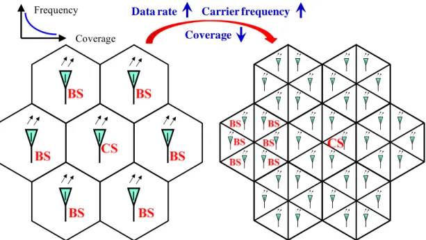
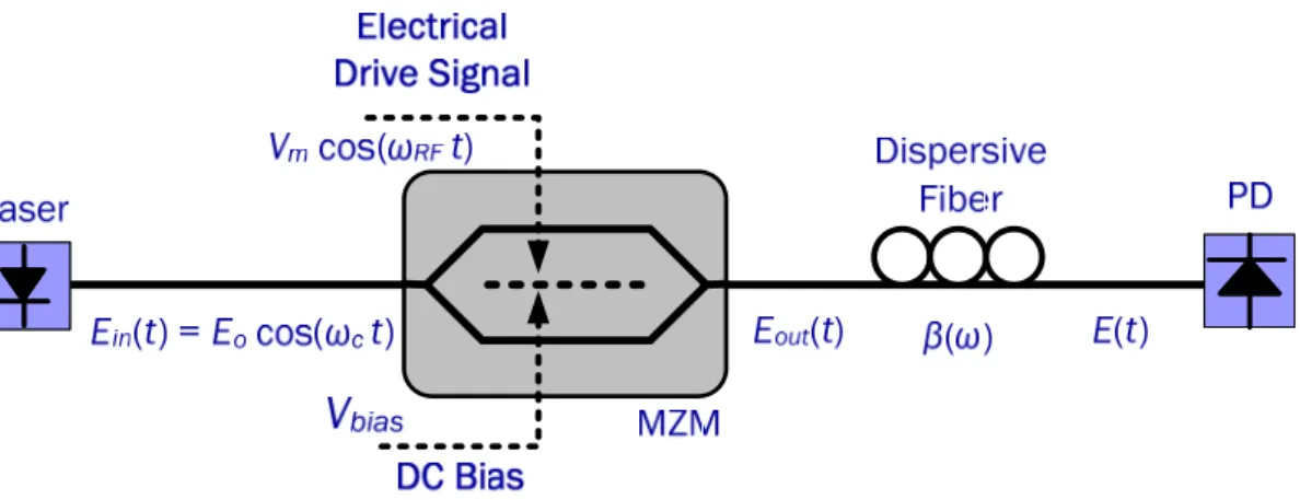
1.1 Review of Radio-over-fiber systemThere are many applications in the microwave band, such as 3G, WiFi (IEEE 80211 b/g/a), and WiMAX are very important for wireless network. When the growth of customers or increase data rate led to insufficient bandwidth in microwave band for the users. Hence, to develop higher frequency microwave, even millimeter-wave is a important issue in the future. Due to the higher frequency millimeter-wave signal has smaller coverage area. Hence, we need a lot of base stations to deliver millimeter-wave signal as shown in Fig. 1-1. In order to saving the system cost and less equipped base stations (BSs) along with a highly centralized central station (CS) equipped with optical and mm-wave components are very importance. Using fiber transmission medium is one of the best solutions because there are wider bandwidth and much less power loss in fiber. Therefore, Radio-over-fiber (ROF) systems are attracted and more interesting for potential use in the future. Broadband wireless communications are shown in Fig. 1-2. ROF technology is a promising solution to provide multi-gigabits/sec service because of using millimeter wave band, and it has wide converge and mobility. The combination of orthogonal frequency-division multiplexing (OFDM) and radio-over-fiber (ROF) systems (OFDM-ROF) is considerable attention for future gigabit broadband wireless communication [1-5]. The high peak to average power ratio (PAPR) and nonlinear distortion of optical transmitter are the main issues raised by OFDM and ROF systems, respectively.
Frequency
Coverage
Data rate Carrier frequency Coverage
Figure 1-1 Basic structure of microwave/millimeter-wave wireless system.
Figure 1-2 the Radio-over fiber system.
1.2 Basic modulation schemes
The optical radio frequency (RF) signal generation using an external Mach-Zehnder modulator (MZM) based on double-sideband (DSB), single-sideband (SSB), and double-sideband with optical carrier suppression (DSBCS) modulation schemes have been demonstrated [1,2,4-8]. Since the optical RF signals are weakly modulated because of the narrow linear region of
MZM, those that have undergone DSB and SSB modulation suffer from inferior sensitivities due to limited optical modulation index (OMI) [4-6,8]. Hence, an optical filter is needed to improve the performance [8]. Furthermore, the DSB signal experiences the problem of performance fading because of fiber dispersion [6]. Among these modulation schemes, DSBCS modulation has been demonstrated to be effective in the millimeter-wave range with excellent spectral efficiency, a low bandwidth requirement for electrical components, and superior receiver sensitivity following transmission over a long distance [6]. However, all of the proposed DSBCS schemes can only support on-off keying (OOK) format, and none can transmit vector modulation formats, such as phase shift keying (PSK), quadrature amplitude modulation (QAM), or OFDM signals, which are of utmost importance for wireless applications.
On the other hand, optical RF signal generations using remote heterodyne detection (RHD) have been also demonstrated [9-10]. The advantage of RHD systems is that the vector signal can be modulated at baseband. Therefore, the bandwidth requirement of the transmitter is low. However, the drawback is that phase noise and wavelength stability of the lasers at both transmitter and receiver should be carefully controlled.
This study proposes a novel method for generating optical direct-detection OFDM-RoF signals using a new DSBCS modulation scheme that can carry vector signals. A frequency multiplication scheme is employed to reduce the requirement of bandwidth of electronic components, which is an important issue at millimeter-wave RoF systems. Benchmarked against the OOK format, the 4-Gb/s 16-QAM OFDM format has the higher spectral efficiency with a sensitivity penalty of under 0.2-dB.
1.3 Motivation
Recently, the wireless communication is focused on millimeter-wave band around 60GHz. The millimeter-wave in this band has some properties for communication such as the short transmission length in the air and broadband bandwidth. It can provide safe communication and transmit high data rate information such as high definition television (HDTV) video signal. However, the electrical components are much more expensive when transmission RF signal is in higher frequency. Hence, the ROF system including frequency multiplication technique and supporting vector signals are required.
Chapter 2
The Concept of New Optical Modulation System
2.1 PrefaceThere are three parts in optical communication systems : optical transmitter, communication channel and optical receiver. Optical transmitter converts an electrical input signal into the corresponding optical signal and then launches it into the optical fiber serving as a communication channel. The role of an optical receiver is to convert the optical signal back into electrical form and recover the data transmitted through the lightwave system. In this chapter, we will do an introduction about the external Mach-Zehnder Modulator (MZM), constructing a model of new ROF system.
2.2 Mach-Zehnder Modulator (MZM)
Direct modulation and external modulation are two modulations of generated optical signal. When the bit rate of direct modulation signal is above 10 Gb/s, the frequency chirp imposed on signal becomes large enough. Hence, it is difficult to apply direct modulation to generate microwave/mm-wave. However, the bandwidth of signal generated by external modulator can exceed 10 Gb/s. Presently, most RoF systems are using external modulation with Mach-Zehnder modulator (MZM) or Electro-Absorption Modulator (EAM). The most commonly used MZM are based on LiNbO3 (lithium niobate) technology. According to the applied electric field, there are two types of LiNbO3 device : x-cut and z-cut. According to number of electrode, there are two types of LiNbO3 device: dual-drive Mach-Zehnder modulator (DD-MZM) and single-drive Mach-Zehnder modulator (SD-MZM) [6].
2.3 Single-drive Mach-Zehnder modulator
The SD-MZM has two arms and an electrode. The optical phase in each arm can be controlled by changing the voltage applied on the electrode. When the lightwaves are in phase, the modulator is in “on” state. On the other hand, when the lightwaves are in opposite phase, the modulator is in “off ” state, and the lightwave cannot propagate by waveguide for output.
2.4 The architecture of ROF system 2.4.1 Optical transmitter
Optical transmitter concludes optical source, optical modulator, RF signal, electrical mixer, electrical amplifier, etc.. Presently, most RoF systems are using laser as light source. The advantages of laser are compact size, high efficiency, good reliability small emissive area compatible with fiber core dimensions, and possibility of direct modulation at relatively high frequency. The modulator is used for converting electrical signal into optical form. Because the external integrated modulator was composed of MZMs, we select MZM as modulator to build the architecture of optical transmitter.
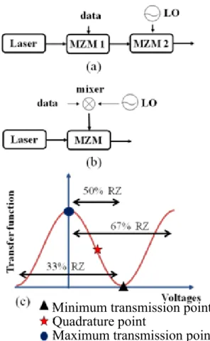
There are two schemes of optical transmitter generated optical signal. One scheme is used two MZM. First MZM generates optical carrier which carried the data. The output optical signal is BB signal. The other MZM generates optical subcarrier which carried the BB signal and then output the RF signal, as shown in Fig. 2-1 (a). The other scheme is used a mixer to get up-converted electrical signal and then send it into a MZM to generate the optical signal, as shown in Fig. 2-1 (b). Fig. 2-1 (c) shows the duty cycle of subcarrier biased at different points in the transfer function.
Maximum transmission point Minimum transmission point Quadrature point
Figure 2-1 (a) and (b) are two schemes of transmitter and (c) is duty cycle of subcarrier biased at different points in the transfer function. (LO: local
oscillator)
2.4.2 Optical signal generations based on LiNbO3 MZM
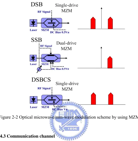
The microwave and mm-wave generations are key techniques in RoF systems. The optical mm-waves using external MZM based on double-sideband (DSB), single-sideband (SSB), and double-sideband with optical carrier suppression (DSBCS) modulation schemes have been demonstrated, as shown in Fig. 2-2. Generated optical signal by setting the bias voltage of MZM at quadrature point, the DSB modulation experiences performance fading problems due to fiber dispersion, resulting in degradation of the receiver sensitivity. When an optical signal is modulated by an electrical
RF signal, fiber chromatic dispersion causes the detected RF signal power to have a periodic fading characteristic. The DSB signals can be transmitted over several kilo-meters. Therefore, the SSB modulation scheme is proposed to overcome fiber dispersion effect. The SSB signal is generated when a phase difference of π/2 is applied between the two RF electrodes of the DD-MZM biased at quadrature point. Although the SSB modulation can reduce the impairment of fiber dispersion, it suffers worse receiver sensitivity due to limited optical modulation index (OMI). The DSBCS modulation is demonstrated optical mm-wave generation using DSBCS modulation. It has no performance fading problem and it also provides the best receiver sensitivity because the OMI is always equal to one. The other advantage is that the bandwidth requirement of the transmitter components is less than DSB and SSB modulation. However, the drawback of the DSBCS modulation is that it can’t support vector signals, such as phase shift keying (PSK), quadrature amplitude modulation (QAM), or OFDM signals, which are of utmost importance in wireless applications.
Figure 2-2 Optical microwave/mm-wave modulation scheme by using MZM.
2.4.3 Communication channel
Communication channel concludes fiber, optical amplifier, etc.. Presently, most RoF systems are using single-mode fiber (SMF) or dispersion compensated fiber (DCF) as the transmission medium. When the optical signal transmits in optical fiber, dispersion will be happened. DCF is use to compensate dispersion. The transmission distance of any fiber-optic communication system is eventually limited by fiber losses. For long-haul systems, the loss limitation has traditionally been overcome using regenerator witch the optical signal is first converted into an electric current and then regenerated using a transmitter. Such regenerators become quite complex and expensive for WDM lightwave systems. An alternative approach to loss
DSB
SSB
Dual-drive MZMDSBCS
Single-drive MZM Single-drive MZMman dire mos ban com 2.4. usu the it h outp can filte test Fig that Fig nagement m ectly witho st RoF sys nd-pass filt mmunicatio Figure .4 Demodu Optical r ually consis microwav has lower t put voltage The BB a n get RF si ered by low After get t the quality . 2-4. Combin t is the mo . 2-3 (b) to makes use out requirin stems are u er (OBPF) on channel 2-3 The m ulation of receiver co sts of the p ve or the m transit tim e. and RF sig ignal by us w-pass filte tting down y, just like ning the tr del of ROF o become th of optical ng its conv using erbiu ) is necessa is shown i model of com optical mi oncludes p photo diode mm-wave sy e. The fun gnals are id sing a mix er (LPF). n-converted bit-error-r ransmitter F system, a he transmit l amplifiers version to t um-doped f ary to filter in Fig. 2-3. mmunicati illimeter-w photo-dete e and the tr ystem, the nction of T dentical aft xer to drop d signal, it rate (BER) with com as shown in tter in the m s, which am the electric fiber ampli r out the A . ion channe wave signa ctor (PD), rans-imped PIN diode TIA is to c ter square-down RF will be se tester or o mmunication n Fig. 2-5. model of R mplify the c domain [ ifier (EDFA ASE noise. l in a RoF al , demodul dance ampl e is usually convert ph -law photo signal to b ent into a s oscilloscop n channel We select ROF system e optical sig 14]. Presen A). An opt The mode system. lator, etc.. lifier (TIA) y used beca hoto-curren detection. baseband t signal teste pe, as show and recei the schem m. gnal ntly, tical el of PD ). In ause nt to We then er to wn in iver, me of
Laser Figure 2-4 Fig MZ data mi 4 The mod gure 2-5 Th ZM ixer BERT el of receiv he model of LO EDFA LPF ver in a RO f ROF syst OBP A mixe OF system. tem. PF fib PD er LO ber D
2.5 The new proposed model of optical modulation system
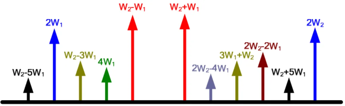
In section 2.3.2, there is an introduction of three traditional modulation schemes to generate optical RF signal. In this work, we propose a new modulation approach to generate optical vector signals by frequency multiplication based on a DSBCS scheme and only using a single-electrode MZM. Fig. 2-6 schematically depicts the optical vector signal generation system. The single-electrode MZM driving signals consist of a sinusoidal signal of frequency f1 modulated with a RF signal and a sinusoidal signal of frequency f2, as indicated in insets (a) and (b) of Fig. 2-6, respectively. To realize the DSBCS modulation scheme, the MZM is biased at the null point. Inset (d) in Fig. 2-6 presents the generated optical spectrum that has two upper-wavelength sidebands (USB1, USB2) and two lower-wavelength sidebands (LSB1, LSB2) with carrier suppression.
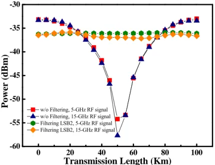
At the base station, the LSB2 subcarrier is filtered out for the upstream data link (inset (f)), and the rest of the signal is sent to local users. After square-law photo detection, the cross term of USB2 and USB1 generates the RF signal at the difference frequency (f2-f1). Concurrently, the cross term of LSB1 and USB2 yields the RF signal at the sum frequency (f2+f1). Here we only consider the RF signal at the sum frequency and a frequency multiplication of optical RF signal can be achieved by proper choosing the frequencies of vector signal and sinusoidal signal. The filtering out of LSB2 subcarrier not only provides an upstream light source but also eliminates performance fading. As presented in Fig. 2-7, a two-tone RF single at frequencies of 5 GHz and 10 GHz is used to simulate the performance fading. After square-law photo detection, the generated RF signals at difference and
sum frequencies of 5 GHz and 15 GHz suffer performance fading before filtering. If an optical filter is utilized to remove anyone of the four optical subcarriers, the fading of both 5-GHz and 15-GHz RF signals can be readily eliminated. Notably, a frequency multiplication (1.5 times after square-law photo detection) scheme is adopted to reduce the cost of the electronic components, especially for RF signals in the millimeter-wave range.
Figure 2-6 Concept of the proposed system. (LD: laser diode, MZM: Mach-Zehnder modulator, SMF: single mode fiber, C: circulator, FBG: fiber
bragg grating, RSOA: reflective semiconductor optical amplifier)
w/o Filtering, 5-GHz RF signal w/o Filtering, 15-GHz RF signal Filtering LSB2, 5-GHz RF signal Filtering LSB2, 15-GHz RF signal 0 20 40 60 80 100 -60 -55 -50 -45 -40 -35 -30 Pow er (d Bm ) Transmission Length (Km)
Figure 2-7 Simulation of RF performance fading versus SMF transmission length.
Chapter 3
The theoretical calculations of proposed system
3.1 Introduce MZMFor MZM with configuration as Fig. 3-1, the output E-filed for upper arm is EU E · a · e∆φ (1) ∆φ
π· π (2)
∆φ is the optical carrier phase difference that is induced by v , where a is the power splitting ratio.
The output E-filed for upper arm is
EL E · √1 a · e∆φ (3) ∆φ is the optical carrier phase difference that is induced by v
∆φ
π· π (4)
The output E-filed for MZM is
ET E · a · b · e∆φ √1 a · √1 b · e∆φ (5) where a and b are the power splitting ratios of the first and second Y-splitters in MZM, respectively. The power splitting ratio of two arms of a balanced MZM is 0.5. The electrical field at the output of the MZM is given by
ET · E · e∆φ e∆φ (6) ET E · cos ∆φ ∆φ · exp j∆φ ∆φ (7) For single electro x-cut MZM. The electrical field at the output is given by EOUT E · cos ∆φ ∆φ · exp j∆φ ∆φ (8) Add time component, the electrical field is
EOUT E · cos ∆φ · cos t (9) where E0 and ωc denote the amplitude and angular frequency of the input optical
carrier, respectively; V t is the applied driving voltage, and ∆φ is the optical carrier phase difference that is induced by between the two arms of the MZM. The loss of MZM is neglected. consisting of an electrical sinusoidal signal and a dc biased voltage can be written as,
cos t (10) where is the dc biased voltage, and are the amplitude and the angular frequency of the electrical driving signal, respectively. The optical carrier phase difference induced by is given by
∆φ
Vπ Vπ ·
π
(11) Eq. (10) can be written as:
EOUT E · cos V V cos ωt
Vπ ·
π
2 · cos ω t E · cos b m · cos ωRFt · cos ω t E · cos ω t · cos b · cos m · cos ωRFt
sin b · sin m · cos ωRFt (12) where V π is a constant phase shift that is induced by the dc biased voltage, and V π is the phase modulation index.
cos x sin θ J x 2 J x cos 2nθ
∞
sin x sin θ 2 J x sin 2n 1 θ
cos x cos θ J x 2 1 J x cos 2nθ ∞
sin x cos θ 2 1 J x cos 2n 1 θ
∞
(13) Expanding Eq. (12) using Bessel functions, as detailed in Eq. (13). The electrical field at the output of the MZM can be written as:
EOUT E · cos · cos · 2 · 1 · m · cos 2 ∞ sin · 2 · 1 · · cos 2 1 ∞ (14) where is the Bessel function of the first kind of order n. the electrical field of the mm-wave signal can be written as
EOUT E · cos · J m · cos ω t E · cos · · cos ∞ 2 π E · cos · · cos 2 ∞ E · sin · · cos ∞ 2 1 E · sin · · cos ∞ 2 1 (15)
Figure 3-1 The principle diagram of the optical mm-wave generation using balanced MZM.
3.2 Theoretical calculation of single drive MZM 3.2.1 Bias at maximum transmission point
When the MZM is biased at the maximum transmission point, the bias voltage is set at 0, and cos 1 and sin 0. Consequently, the electrical field of the mm-wave signal can be written as
· · cos · · cos ∞ 2 · · cos 2 ∞ (16)
The amplitudes of the generated optical sidebands are proportional to those of the corresponding Bessel functions associated with the phase modulation index . With the amplitude of the electrical driving signal equal to , the
maximum is . As 0 , the Bessel function for 1 decreases and increases with the order of Bessel function and m, respectively, as shown in Figure 3-2. , , , and are 0.5668, 0.2497, 0.069, and 0.014, respectively. Therefore, the optical sidebands with the Bessel function higher than can be ignored, and Eq. (14) can be further simplified to · · cos · · cos 2 · · cos 2 · · cos 4 · · cos 4 (17) 0 2 4 6 8 10 -0.5 0.0 0.5 1.0 m
J0
J1
J2
J3
Figure 3-2 The different order of Bessel functions vs. m.3.2.2 Bias at quadrature point
V
, and cos √ and sin √ . Consequently, the electrical field of the mm-wave signal can be written as
EOUT 1 √2· E · J m · cos ω t 1 √2· E · J m · cos ω ωRF t 1 √2· E · J m · cos ω ωRF t 1 √2· E · J m · cos ω 2ωRF t π 1 √2· E · J m · cos ω 2ωRF t π 1 √2· E · J m · cos ω 3ωRF t π 1 √2· E · J m · cos ω 3ωRF t π (18)
3.2.3 Bias at null point
When the MZM is biased at the null point, the bias voltage is set at V , and cos 0 and sin 1. Consequently, the electrical field of the mm-wave signal using DSBCS modulation can be written as
EOUT E · J m · cos ω ωRF t E · J m · cos ω ωRF t E · J m · cos ω 3ωRF t π E · J m · cos ω 3ωRF t π E · J m · cos ω 5ωRF t E · J m · cos ω 5ωRF t (19)
3.3 Theoretical calculations and simulation results 3.3.1 The generated optical signal
The theoretical calculations of proposed system, the driving RF signal consisting of an electrical sinusoidal signal and a dc biased voltage can be written as
cos t cos t (20)
where is the dc biased voltage, , and , are the amplitude and the angular frequency of the electrical driving signals, respectively. The optical carrier phase difference induced by is given by
· cos
V cos t cos t
· cos cos t cos t (21)
where is a constant phase shift that is induced by the dc biased voltage, and V , V is the phase modulation index.
· cos · cos cos t cos t
· sin · sin cos t cos t
· cos cos m cos cos cos
sin cos sin cos
· sin sin cos t cos cos t
cos cos t sin cos t (22) When the MZM is biased at the null point, the bias voltage is set at V , and cos 0 and sin 1. Consequently, the electrical field of the mm-wave signal using DSBCS modulation can be written as
sin cos t cos cos t
cos cos t sin cos t (23) First, to expand equation sin cos t cos cos t
sin cos t cos cos t 2 1 J cos 2n 1 t ∞ · J 2 1 J cos 2n t ∞ 2J cos t 2J cos 3 t · J 2J cos 2 t 2J cos 4 t (24) The optical sidebands with the Bessel function higher than can be ignored. Consequently, the electrical field can be written as
sin cos t cos cos t
2J J cos t 2J J cos 3 t 4J J ·1 2 cos 2 t cos 2 t 4J J ·1 2 cos 3 2 t cos 3 2 t (25) Add time component cos t
sin cos t cos cos t cos t
2J J cos t cos t
2J J cos 3 t cos t
4J J ·1
2 cos 2 t cos 2 t cos t
4J J ·1
2 cos 3 2 t cos 3 2 t cos t
(26)
J J , 2J J , 4J J , and 4J J are
4J J can be ignored, and Eq. (14) can be further simplified to
sin cos t cos cos t cos t
J J cos t cos t J J cos 3 t cos 3 t J J cos 2 t cos 2 t J J cos 2 t cos 2 t (27) 0.0 0.2 0.4 0.6 0.8 1.0 1.2 1.4 1.6 1.8 -0.1 0.0 0.1 0.2 0.3 0.4
m
1,m
2 J0J1 J0J3 J1J2 J2J3 Figure 3-3 The different order of Bessel functions vs. m.cos cos sin cos 2 1 cos 2 ∞ · 2 1 cos 2 1 ∞ 2 cos 2 2 cos 4 · 2 cos 2 cos 3 2 cos 2 cos 3 4 ·1 2 cos 2 cos 2 4 ·1 2 cos 3 2 cos 3 2 (28) Add time component cos
cos cos sin cos cos
2 cos cos
2 cos 3 cos
4 ·1
2 cos 2 cos 2 cos
4 ·1
2 cos 3 2 cos 3 2 cos
cos cos
cos 3 cos 3
cos 2 cos 2
cos 2 cos 2 (29)
The output electrical filed can be rewritten as
cos cos sin cos t · cos cos cos 3 cos 3 cos 2 cos 2 cos 2 cos 2 cos cos cos 3 cos 3 cos 2 cos 2 cos 2 cos 2 (30) Figure 3-4 Illustration of the optical spectrum at the output of the MZM.
( 6 )
The commercial software, VPI WDM-TransmissionMaker© 5.0, is used to simulate numerically the power ratio. Fig. 3-5 shows the optical power ratio (OPR, , ) as a function of MI. The , is defined as
,
(31) where and are the optical powers of the sideband frequency at
respectively. As MI falls from one to zero, the optical power ratios are improved. 0.0 0.2 0.4 0.6 0.8 1.0 0 10 20 30 40 50 60 70 80
MI
Theoretical P
10,+21,P
10,+12Numerical P
10,+21,P
10,+12Theoretical P
10,30,P
10,03Numerical P
10,30,P
10,03Power (10dB/Div.)
Figure 3-5 Illustration of the optical spectrum at the output of the MZM.3.3.2 The generated electrical signal
After square-law detection using an ideal PD with responsivity R, the photocurrent can be expressed as
· | | (32)
The RF signal is E ·
J J 2J J J 2J J 4J J J · cos 2 t 2J J J J 2J J J J 2J J J J 2J J J J 2J J J J 2J J J J · cos t cos t J J 2J J J 2J J 4J J J · cos 2 t 2J J J J 2J J J J 2J J J J · cos 3 t cos 3 t 2J J J 2J J J 2J J J J 2J J J J · cos 2 2 t 2J J J 2J J · cos 4 t J J 2J J J J · cos 2 4 t 2J J J J · cos 5 t RF (33)
Figure 3-6 Illustration of the electrical spectrum of generated BTB mm-wave signals using MZM after square-law PD detection. ( 6 )
Fig. 3-7 shows the RF signal power ratio (RFPR, , ) as a function of MI. The , is defined as
,
(34) where and are the RF signal powers of the frequency at 1 ·
1 · and the frequency at · · ,respectively. The RF signal power at sum and subtract frequencies are the same, so do not consider the , term.
0.0 0.2 0.4 0.6 0.8 1.0 -10 0 10 20 30 40 50 60 70 80 90 100 110
MI
P11,20,P11,02 P11,-22 P11,31,P11,-31 P11,40 P11,-42 P11,51,P11,-51Power (10dB/Di
v.)
Figure 3-7 The RF signal power ratio (RFPR, , ) as a function of MI.
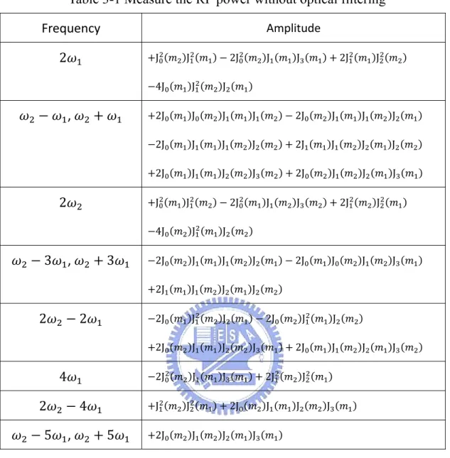
Table 3-1 Measure the RF power without optical filtering Frequency Amplitude 2 J J 2J J J 2J J 4J J J , 2J J J J 2J J J J 2J J J J 2J J J J 2J J J J 2J J J J 2 J J 2J J J 2J J 4J J J 3 , 3 2J J J J 2J J J J 2J J J J 2 2 2J J J 2J J J 2J J J J 2J J J J 4 2J J J 2J J 2 4 J J 2J J J J 5 , 5 2J J J J
3.3.3 Consider dispersion effect
When optical RF signals are transmitted over a single-mode fiber with dispersion, a phase shift to each optical sideband relative to optical carrier is induced. The propagation constant of the dispersion fiber can be expressed as
where is the derivative of the propagation constant evaluated at . The effect of high order fiber dispersion at 1550-nm band is neglected. For carrier tones with central frequency at , we have
(36) and
· D (37) where c is light speed in free space, D is the chromatic dispersion parameter, and is the frequency of the optical carrier. For a standard single-mode fiber, D is 17-ps/(nm.km). The fiber loss is ignored. Therefore, after transmission over a single-mode fiber of length z, the electrical field can be written as
· cos 1 2 cos 1 2 cos 1 2 cos 1 2 (38)
After square-law photo detection, the RF signal can be expressed as · DC RF
2 · cos 1
2 · cos 1
2 · cos 1 2 · cos 1 2 2 · cos 1 2 · cos 1 2 2 · cos 1 2 · cos 1 2 (39)
The RF signal at the substrate frequency :
I J J J J · cos t 1 2 1 2 cos t 1 2 1 2 (40) Define c t d 1 2 1 2 1 2 (41) The RF signal at the substrate frequency can be written as
I J J J J · cos c d cos c d I 2J J J J · cos c cos d 2J J J J · cos 1 2 · cos t (42)
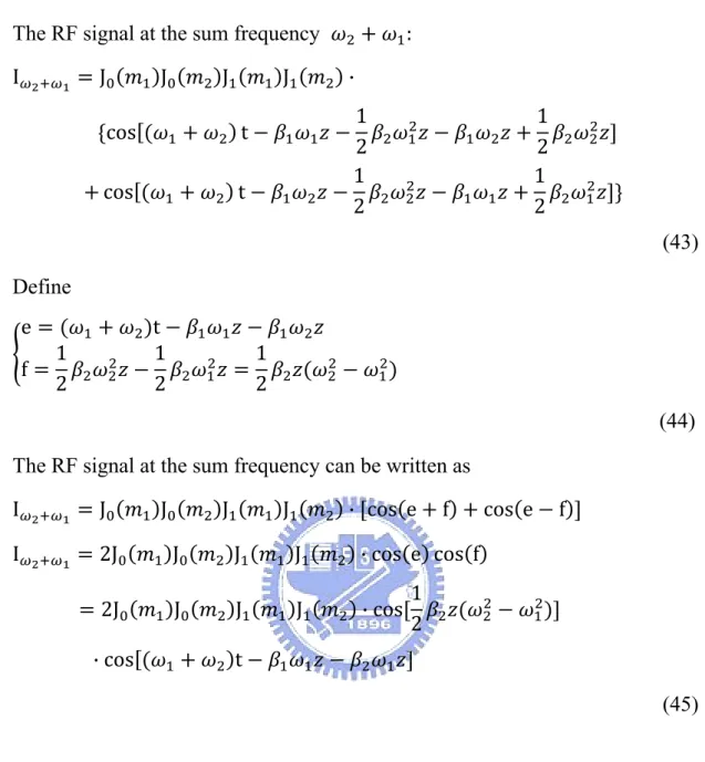
The RF signal at the sum frequency : I J J J J · cos t 1 2 1 2 cos t 1 2 1 2 (43) Define e t f 1 2 1 2 1 2 (44) The RF signal at the sum frequency can be written as
I J J J J · cos e f cos e f I 2J J J J · cos e cos f 2J J J J · cos 1 2 · cos t (45)
Fig. 3-8 and Fig. 3-9 show the numerical simulation and theoretical solutions, the RF fading problem with the same results. Fig. 3-8 RF signal is driving 5 GHz and 30 GHz sinusoidal. Fig. 3-9 shows the results after 50km SMF transmission.
0 10 20 30 40 50 -50 -40 -30 -20 -10 0 10
Transmission Length (km)
25G Numerical
35G Numerical
Theoretical
P owe r (10dB/Div.) Figure 3-8 shows the numerical and theoretical solution for RF signal fadingissue after transmission.
30 35 40 45 50 55 60 -50 -40 -30 -20 -10 0 10
Frequency (GHz)
Numerical
Theoretical
Pow er ( 1 0d B /D iv .) Figure 3-9 RF power vs. .3.4 The generated optical signal using optical filtering 3.4.1 Analysis of the generated signal
When we use fiber grating, the equation for the optical spectrum is · J J · cos t cos t J J cos 3 t cos 3 t J J cos 2 t cos 2 t J J cos 2 t cos 2 t J J · cos t cos t J J cos 3 t cos 3 t J J cos 2 t cos 2 t J J cos 2 t cos 2 t (46) Figure 3-10 shows the optical spectrum when the LSB1 is filter out.
Figure 3-11 shows the optical spectrum when the LSB2 is filter out.
After square-law detection, the photocurrent can be expressed as E · · J J 1 · J J J 2J J 2 2 · J J J · cos 2 t 1 · J J J J 1 · J J J J 1 · J J J J 2J J J J 2J J J J 2J J J J · cos t · J J J J 1 · J J J J 1 · J J J J 2J J J J 2J J J J 2J J J J · cos t · J J 1 · J J J 2J J 2 2 · J J J · cos 2 t 1 · J J J J 1 · J J J J 2J J J J · cos 3 t cos 3 t
1 · J J J 1 · J J J 2J J J J 2J J J J · cos 2 2 t 1 · J J J 2J J · cos 4 t J J 2J J J J · cos 2 4 t 2J J J J · cos 5 t RF (47)
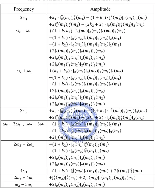
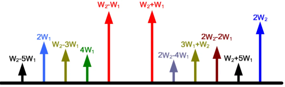
Table 3-2 Measure the RF power with optical filtering Frequency Amplitude 2 · J J 1 · J J J 2J J 2 2 · J J J 1 · J J J J 1 · J J J J 1 · J J J J 2J J J J 2J J J J 2J J J J · J J J J 1 · J J J J 1 · J J J J 2J J J J 2J J J J 2J J J J 2 · J J 1 · J J J 2J J 2 2 · J J J 3 , 3 1 · J J J J 1 · J J J J 2J J J J 2 2 1 · J J J 1 · J J J 2J J J J 2J J J J 4 1 · J J J 2J J 2 4 J J 2J J J J 5 2J J J J
Figure 3-12 Illustration of the electrical spectrum of generated BTB mm-wave signals when the LSB1 is filter out. ( 6 )
Figure 3-13 Illustration of the electrical spectrum of generated BTB mm-wave
3.4.2 The effects of fiber dispersion
Consider fiber dispersion effect, the electrical field can be written as
· · J J cos ω t 1 2 J J cos ω t 1 2 · J J cos ω t 1 2 J J cos ω t 1 2 (48) After square-law photo detection, the RF signal can be expressed as
E · DC RF 2J J J J · · cos ω t 1 2 · · cos ω t 1 2 2J J J J · cos ω t 1 2 · cos ω t 1 2 2J J J J · · cos ω t 1 2 · cos ω t 1 2 2J J J J · cos ω t 1 2 · · cos ω t 1 2 (49)
The RF signal at the substrate frequency : I J J J J · · cos t 1 2 1 2 cos t 1 2 1 2 (50) Define a t b 1 2 1 2 1 2 (51) The RF signal at the substrate frequency can be written as
I J J J J
· · cos a b · cos a b 1 · cos a b
I J J J J
· 2 cos a cos b 1 · cos a b
J J J J · 2 cos 1 2 · cos t 1 cos t 1 2 (52) The RF signal power at the substrate frequency can be written as
P J J J J · A B 2AB · cos θ J J J J · 2 cos 1 2 1 2 2 cos 1 2 · 1 · cos θ
The RF signal at the sum frequency I J J J J · cos t 1 2 1 2 cos t 1 2 1 2 (54) Define a t b 1 2 1 2 1 2
The RF signal at the sum frequency can be written as
I J J J J
· cos a b cos a b cos a b
I J J J J
· 2 cos a cos b cos a b
J J J J · 2 cos 1 2 · cos t cos t 1 2 (55) Or I J J J J
· cos a b cos a b cos a b
I J J J J · 2 cos 1 2 · cos t cos t 1 2 A · cos t θ B · cos t θ θ (56)
The RF signal power at the sum frequency can be written as P J J J J · A B 2AB · cos θ J J J J · 2 cos 1 2 2 2 cos 1 2 · · cos θ (57) Or P J J J J · A B 2AB · cos θ J J J J · 2 cos 1 2 2 2 cos 1 2 · · cos θ (58) Because grating only filter out LSB1 or LSB2 at the same time, so the equation of the RF signal power at the sum and substrate frequency are the same. The RF signal power can be written as
P P J J J J · 2 cos 1 2 1 2 2 cos 1 2 · 1 · cos θ (59) If grating is filter out 28dB, 20Log 28, 0.04.
0 10 20 30 40 50 -50 -40 -30 -20 -10 0 10
Transmission length (Km)
Numerical 25GHz
Numerical 35GHz
Theoretical
Pow
er (10dB/Div.
)
Figure 3-14 shows the RF signal power vs. transmission length when the LSB1is filter out. 0 10 20 30 40 50 -50 -40 -30 -20 -10 0 10
Transmission length (Km)
Numerical 25GHz
Numerical 35GHz
Theoretical
Pow
er (10dB/Div.
)
Figure 3-15 shows the RF signal power vs. transmission length when the LSB23.5 The optimal optical power ratio condition 3.5.1 Signal without optical filtering
We assume the output e-filed of LSB2, LSB1, RSB1 and RSB2 are E , E , E and E respectively. When we use single drive MZM and set the bias point of MZM at Vπ and then the e-filed is
E E , E E (60)
For the PSK signal that the total power can be written as
E E E E P
2E 2E P (61)
The optical field is then detected using and ideal square-law photodetector, and the RF signals generated are mathematically evaluated as follows:
2E 2E E · E E · E E · E E · E
The f f RF signal term is
E · E E · E 2E · E (62)
Where E P E for PSK signal The RF signal become
2E · P E (63)
The maximum of RF signal power originates from
2E · P E
′
0 (64)
To solve the differential equation we would get the e-filed E √P 2⁄ , E √P 2⁄
E : E : E : E 1: 1: 1: 1 (65)
The optical powers are
For the OOK signal that the total power can be written as
2E E E 2E P
4E 2E P (67)
The f f RF signal term is
E · E E · E 2E · E (68)
Where E P E for OOK signal The RF signal become
2E · P E (69)
The maximum of RF signal power is happened in
2E · P E
′
0 (70)
To solve the differential equation we would get the e-filed E √P 2⁄ , E P 8⁄
and
E : E : E : E 1: √2: √2: 1 (71)
The optical powers are
I I 2E P 4⁄
I I E P 4⁄ (72)
and
I : I : I : I 1: 1: 1: 1 (73)
When the optical signal without filtering, the optimal SOPR of both PSK and OOK RF signals is 0-dB.
Figure 3-16 shows optical spectrum without fiber grating filter out.
Figure 3-17 the e-filed power for BPSK signal between zero and one.
Figure 3-18 the e-filed power for OOK signal between zero and one.
3.5.2 When the LSB2 or LSB1 is filter out
Using fiber grating to remove LSB1 and getting maximum output RF signal condition for PSK signal is
E : E : E 1: 1: √2 (74)
The optical power equal
I : I : I 1: 1: 2 (75)
and for OOK signal
E : E : E 1: 1: 1 (76)
The optical power equal
I : I : I 1: 1: 2 (77)
The optimal SOPR of both PSK and OOK RF signals is 3-dB when the LSB2 with filtering.
Using fiber grating to remove LSB1 and getting maximum output RF signal condition for PSK signal is
E : E : E 1: √2: 1 (78)
The optical power equal
I : I : I 1: 2: 1 (79)
And for OOK signal
E : E : E 1: 2: 1 (80) The optical power equal
I : I : I 1: 2: 1 (81)
The optimal SOPR of both PSK and OOK RF signals is -3-dB when the LSB1 with filtering.
Figure 3-19 shows optical spectrum when the LSB2 is filter out.
Figure 3-20 shows optical spectrum when the LSB1 is filter out.
Chapter 4
Experimental demonstration of the proposed system
4.1 prefaceIn chapter 3, we provide the theoretical and numerical results for the concept of proposed system. Therefore, the result can be tried to apply to the radio-over-fiber system. In this chapter, we will build the experimental setup for the propose system based on DSBCS modulation. Figure 4-1 shows the optical spectrum for the fiber Bragg grating reflection and transmission.
Figure 4-1 the optical spectrum for the fiber Bragg grating reflection and
transmission. 1555.65-20 1555.7 1555.75 1555.8 1555.85 -10 0 R efl ec tio n (d B ) Wavelength (nm) 1555.65 1555.7 1555.75 1555.8 1555.85-30 -20 -10 0 T rans m is si on ( dB ) Reflection Transmission
4.2 Experimental results for optical signal without optical filtering 4.2.1 Experiment setup
Figure 4-2 displays the experimental setup for optical vector signal generation and transmission using a single-electrode MZM. The continue wave laser source about 1550nm is generation using tunable laser. The laser source is then passed through a polarization controller to achieve output optical power is a maximum when the MZM is biased at full point. The OOK/BPSK signal is a 1.25-Gb/s pseudo random binary sequence (PRBS) signal with a word length of 231-1 and is up-converted using a 5-GHz sinusoidal signal (f1). The 625-MSym/s QPSK signal at 5-GHz is generated using an arbitrary waveform generator. Then the RF OOK/BPSK/QPSK signals are combined with a 10-GHz sinusoidal signal (f2). This combined RF signal is fed into single-electrode MZM and the MZM is bias the null point. The generated optical spectrum that has two upper-wavelength sidebands (USB1, USB2) and two lower- wavelength sidebands (LSB1, LSB2) with carrier suppression. The generated optical signal is amplified by EDFA and then filtered by an optical tunable filter with a bandwidth of 38GHz. The input EDFA optical power is fixed -20dBm. The power of optical RF signal which entered fiber is set to less than 0 dBm to reduce the effect of both fiber nonlinearity and dispersion changing the duty cycle of optical microwaves. After transmitted over standard single mode fiber (SSMF), the transmitted optical microwave signal is converted into an electrical microwave signal by a PIN PD with a 3 dB bandwidth of 38 GHz, and the converted electrical signal is amplified by an electrical amplifier. If we would measure the RF signal at the subtract frequency, the RF signal is then passed through the electrical bandpass filter at
5GHz. The center frequency of bandpass filter is 15GHz when we would measure the RF signal at the sum frequency. After the photo receiver, the optical signal generates two RF signals with a subtract frequency of 5 GHz (f2-f1) and a sum frequency of 15 GHz (f1+f2), respectively. Insets (i) and (ii) of
Figure 4-2 show the receiver architectures of RF OOK/BPSK and QPSK signals, respectively. The RF OOK/BPSK signal is down-converted to baseband signal and directly tested by a BER tester. The RF QPSK signal is down-converted to 5 GHz by a 10 GHz oscillator and a mixer to realize intermediate frequency (IF) demodulation. A digital real-time oscilloscope (Tektronix DPO71254) stores the waveform and an off-line digital signal processing (DSP) program using Matlab is employed to demodulate the QPSK signal. For QPSK signal, the bit error rate (BER) performance is calculated from the measured modulation error ratio (MER). The MER is defined as MER I I I QQ Q , where Ir and Qr represent the demodulated in-phase
and quadrature-phase symbols, and Io and Qo are the ideal normalized in-phase
and quadrature-phase QPSK symbols. The optical intensity of the data-modulated subcarriers (5 GHz) relative to that of the sinusoidal subcarrier (10 GHz) can be easily tuned by adjusting the input electrical power to optimize the performance of the optical RF signals.
Figure 4-2 shows the experimental setup to receive sum frequency.
4.3.2 Optimal condition for RF signal
Fig. 4-3 and Fig. 4-4 show the optical spectrums in different SOPR (SOPR= Ps/Pd, Ps and Pd are the optical powers of the 10-GHz subcarrier and the 5-GHz
data-modulated subcarrier, respectively.) for BPSK and OOK signal. The BER curves of BPSK and OOK signal at substrate frequency shown in Fig. 4-5 and Fig. 4-6. When we consider the RF signal at sum frequency. The BER curves and eye diagrams of BPSK are shown in Fig 4-7 and Fig. 4-8. For OOK signal are shown in Fig. 4-9 and Fig. 4-10. Fig. 4-11 and Fig. 4-12 present the measured receiver sensitivity at a bit error rate (BER) of 10-9 and simulated Q-factor or MER of BPSK and OOK or QPSK RF signals as function of the ratio of the sinusoidal subcarrier power to the data-modulated subcarriers
power The modulated index of the 10-GHz sinusoidal signal (MI=Vp-p/2VΠ) is
set to 0.1 and adjusted SOPR to 0dB by changing the electrical power of the 5-GHz data. And then is adjusted the electrical power of 10-GHz sinusoidal signal to changing SOPR. For RF signal generation without filtering, the optimal SOPR of both BPSK and OOK RF signals is 0 dB.
1554.7 1554.8 1554.9 1555.0 1555.1 1555.2 -70 -60 -50 -40 -30 Wavelength (nm) Po we r ( 1 0d B/ Di v. ) 1554.7 1554.8 1554.9 1555.0 1555.1 1555.2 -70 -60 -50 -40 -30 Wavelength (nm) Po we r ( 1 0d B/ Di v. ) 1554.7 1554.8 1554.9 1555.0 1555.1 1555.2 -70 -60 -50 -40 -30 Wavelength (nm) Po we r ( 1 0d B/ Di v. ) 1554.7 1554.8 1554.9 1555.0 1555.1 1555.2 -70 -60 -50 -40 -30 Wavelength (nm) Po we r ( 1 0d B/ Di v. ) 1554.7 1554.8 1554.9 1555.0 1555.1 1555.2 -70 -60 -50 -40 -30 -20 Wavelength (nm) Po we r ( 1 0d B/ Di v. ) 1554.7 1554.8 1554.9 1555.0 1555.1 1555.2 -70 -60 -50 -40 -30 Wavelength (nm) Po we r ( 1 0d B/ Di v. ) 1554.7 1554.8 1554.9 1555.0 1555.1 1555.2 -70 -60 -50 -40 -30 -20 Wavelength (nm) Po we r ( 1 0d B/ Di v. )
1554.7 1554.8 1554.9 1555.0 1555.1 1555.2 -70 -60 -50 -40 -30 Wavelength (nm) Po we r ( 1 0d B/ Di v. ) 1554.7 1554.8 1554.9 1555.0 1555.1 1555.2 -70 -60 -50 -40 -30 Wavelength (nm) Po we r ( 1 0d B/ Di v. ) 1554.7 1554.8 1554.9 1555.0 1555.1 1555.2 -70 -60 -50 -40 -30 Wavelength (nm) Pow er ( 10d B/ D iv. ) 1554.7 1554.8 1554.9 1555.0 1555.1 1555.2 -70 -60 -50 -40 -30 Wavelength (nm) Pow er ( 10d B/ D iv. ) 1554.7 1554.8 1554.9 1555.0 1555.1 1555.2 -70 -60 -50 -40 -30 Wavelength (nm) Pow er ( 10d B/ D iv. ) 1554.7 1554.8 1554.9 1555.0 1555.1 1555.2 -70 -60 -50 -40 -30 Wavelength (nm) Pow er ( 10d B/ D iv. ) 1554.7 1554.8 1554.9 1555.0 1555.1 1555.2 -70 -60 -50 -40 -30 Wavelength (nm) Pow er ( 10d B/ D iv. )
-25 -24 -23 -22 -21 -20 -19 -18 -17 10 9 8 7 6 5 4 3 2 -9dB -6dB -3dB +0dB +3dB +6dB +9dB -Log(BER) Power(dBm) Figure 4-5 the BER curves for BPSK at 5GHz.
-23 -22 -21 -20 -19 -18 -17 -16 -15 10 9 8 7 6 5 4 3 2 -9dB -6dB -3dB +0dB +3dB +6dB +9dB -Log(BER) Power(dBm) Figure 4-6 the BER curves for OOK at 5GHz.
-24 -23 -22 -21 -20 -19 -18 -17 10 9 8 7 6 5 4 3 2 -9dB -6dB -3dB +0dB +3dB +6dB +9dB -Log(BER) Power(dBm) Figure 4-7 the BER curves for BPSK at 15GHz.
SOPR=-9dB SOPR=-6dB
SOPR=-3dB SOPR=0dB SOPR=+3dB
SOPR=+6dB SOPR=+9dB
-23 -22 -21 -20 -19 -18 -17 -16 -15 -14 10 9 8 7 6 5 4 3 2 -9dB -6dB -3dB +0dB +3dB +6dB +9dB -Log(BER) Power(dBm) Figure 4-9 the BER curves for OOK at 15GHz
Figure 4-10 the eye diagrams for BPSK at 15GHz.
-9 -6 -3 0 3 6 9 12 -20 -18 -16 -14 -12 BPSK,w/o filtering OOK, w/o filtering
Sensiti
v
ity (dBm)
SOPR(dB)
Figure 4-11 measured receiving sensitivity at BER=10-9 of OOK and BPSK
signals versus SOPR.
-9 -6 -3 0 3 6 9 24 26 28 30 32 0 3 6 9 12 15
MER (
d
B)
Q Facter (dB)
SOPR(dB)
QPSK,w/o filtering
BPSK,w/o filtering
OOK ,w/o filtering
Figure 4-12 the simulation result of MER and Q factor for BPSK, OOK and
4.3.3 Transmission results
Fig. 4-13 plots the BER curves of OOK, BPSK and QPSK signals without optical filtering using optimal SOPRs following 50-km SMF transmission. The receiver sensitivity penalty of RF signals increases with transmission length of SMF due to fiber dispersion. Fig. 4-14 and Fig. 4-15 show the eye diagrams for BPSK and OOK become smaller as transmission length increases. For QPSK signal the constellation and IQ eye diagram becomes smaller as transmission length increases is shown in Fig. 4-16.
-24
-22
-20
-18
-16
-14
-12
11
10
9
8
7
6
5
4
3
2
OOK , 0km OOK , 25km OOK , 50km BPSK, 0km BPSK, 25km BPSK, 50km QPSK, 0km QPSK, 25km QPSK, 50km-Log(BER)
Power(dBm)
Figure 4-13 the BER curves of OOK, BPSK and QPSK signals.Figure 4-14 the eye diagrams for BPSK signal w/o filtering.
Figure 4-15 the eye diagrams for OOK signal w/o filtering.
-0.06 -0.04 -0.02 0.00 0.02 0.04 0.06 -0.06 -0.04 -0.02 0.00 0.02 0.04 0.06 Q amplitude (a.u.) I amplitude (a.u.) -0.06 -0.04 -0.02 0.00 0.02 0.04 0.06 -0.06 -0.04 -0.02 0.00 0.02 0.04 0.06 Q amplitude (a.u.) I amplitude (a.u.) Figure 4-16 the constellations and I/Q eye diagram for QPSK signal.
4.4 Experimental setup for optical signal with optical filtering
The generated optical spectrum that has two upper-wavelength sidebands and two lower-wavelength sidebands with carrier suppression. After square-law photo detection, the optical RF signals have RF fading problem. The reason is that there are two sources for the generated 5-GHz or 15-GHz RF signal. For the 15-GHz RF signal, the cross terms of USB2*LSB1 and USB1*LSB2 will contribute the power of that. After standard single mode fiber (SMF) transmission, the relative phase of the two cross-term signal wills change with transmitted length, resulting in performance fading. If an optical filter is utilized to remove anyone of the four optical subcarriers, the fading of both 5-GHz and 15-GHz RF signals can be readily eliminated. Notably, a frequency multiplication (1.5 times after square-law photo detection) scheme is adopted to reduce the cost of the electronic components, especially for RF signals in the millimeter-wave range.
4.4.1 Experiment setup
Fig. 4-17 displays the experimental setup for optical vector signal generation and transmission using a single-electrode MZM. At the remote node, a fiber Bragg grating filter removes the LSB2 or LSB1. After the photo receiver, the optical signal generates two RF signals with a difference frequency of 5 GHz (f2-f1) and a sum frequency of 15 GHz (f1+f2), respectively. In this study, we
only consider the generated RF signal at 15 GHz. Insets (i) and (ii) of Fig. 4-17 show the receiver architectures of RF OOK/BPSK and QPSK signals, respectively.
Figure 4-17 shows the experiment setup w/ optical filtering.
4.4.2 RF signals at sum frequency
Fig. 4-18 plots the optical spectrums for BPSK signals with filter out LSB2. Fig. 4-19 shows the simulation result of MER and Q factor for BPSK OOK and QPSK signals with optical filter out LSB2. The optimal SOPR is 3 dB. Fig. 4-20 shows the experimental results of receiver sensitivity at BER of 10-9. Fig. 4-21 display the eye diagrams of BPSK signal with optical filter out LSB2. Fig. 4-22 plots the optical spectrums for BPSK signals with filter out LSB1. Fig. 4-23 shows the experimental results of receiver sensitivity at BER of 10-9. Fig. 4-24 display the eye diagrams of BPSK signal with optical filter out LSB1. The experimental result is consistent with simulation.