Photosensor application of amorphous InZnO-based thin film
transistor
Po-Tsun Liu*
a, Yi-Teh Chou
b, Li-Feng Teng
ba
Department of Photonics & Display Institute, National Chiao Tung University, Hsinchu, Taiwan,
30010, R.O.C
b
Department of Photonics & Institute of Electro-Optical Engineering, National Chiao Tung
University, Hsinchu, Taiwan, 30010, R.O.C
* Corresponding author: [email protected]
ABSTRACT
Thin film transistor (TFT) device structure with transparent conductive oxide semiconductor is proposed for the photosensor application. The adoption of TFT-based photosensor device also is promising to be integrated with pixel-array circuits in a flat panel display and realize the system-on-panel (SoP) concept. The photosensitive TFT device can be applied to sense the ambient light brightness and then give the feedback to the backlight system adjusting the backlight intensity for the power-saving green displays. In this work, we studied the photosensitivity of amorphous indium zinc oxide (a-IZO) TFT to ultraviolet light. The a-IZO-based semiconductors have been paid much attention due to their uniform amorphous phase and high field-effect carrier mobility characteristics. The obvious threshold voltage shift was observed after light illumination, and exhibited slow recovery while returning to initial status after removing the light source. This mechanism for the photoreaction is well explained by the dynamic equilibrium of charge exchange reaction between O2(g) and O2- in the backchannel region of IZO-based films. An electrical trigger using charge pumping
method is used to confirm the proposed mechanism and accelerate photoreaction recoverability for the first time. Using knowledge of photoreaction behavior, an operation scheme of photosensing elements consist of a-IZO TFTs is also demonstrated in this paper.
Keywords: photosensor, power-saving, amorphous indium zinc oxide (a-IZO) TFT, electrical trigger method
1. INTRODUCTION
As the development of flat panel displays grows rapidly, the thin film transistor (TFT) technologies have been widely used as switching devices in active-matrix liquid crystal display (AM-LCD) or integrating in peripheral circuits to apply driving signals. System-on-panel (SoP) concept also has been proposed to enable various functional devices, such as driver, sensor, memory and controller devices, to be integrated on a single panel for achieving high-performance, low-cost and more compact display products. Not only for large size display but also for portable display products, the demands for novel electronic display apparatus are mainly toward high resolution and low power consumption. The adoption of excellent characteristic semiconductor materials instead of typically-used silicon as a channel layer of TFT can effectively increase the resolution of display and reduce the power consumption. [1-3] The introduction of photosensor devices to display peripheral circuits can adjust a luminance of display panel in accordance with ambient light intensity, and thereby power consumption can be reduced further.[4] To realize the SoP technology, the electronic devices with different functions are preferred to have the same or similar device structure for manufacture with ease. However, photosensor devices generally appear in the form of photodiodes or photo-resistors at present, which is difficult to be embedded directly to the TFT pixel circuits. Also, the photosensor devices discussed above strongly relied on the sensitivity characteristics of photo-reaction materials and process temperature in fabrication. Those surely limit the application and manufacture cost. In this work, TFT-based photosensor device with transparent conductive oxide (TCO) is studied. Such amorphous TCOs as indium zinc oxide (a-IZO) or gallium doped a-IZO (a-IGZO) not only have great potential to form a uniform amorphous phase but also include highly conducting carriers and exhibit high
effect carrier mobility characteristics. [5-8] Although the a-IZO film is transparent and has the energy band gap up to 3.05 eV, visible light sensitivity was still found in the a-IZO due to the structure defects inside. The photosensitivity of single a-IZO film itself has been reported in previous reports, but most of them were only focused on the analysis of thin film characteristics and few for the device aspect.[9-10] The present work proposes a reasonable physical mechanism to describe the photoreaction behavior of the a-IZO TFT device. Using knowledge of the photoreaction mechanism, potential applications for photosensor devices are depicted in this study for the first time. The photosensitivity of a-IZO TFTs also extends its application for light sensors in flat panel displays.
2. EXPERIMENTS
Our experimental work was based on the inverted coplanar structure TFT device fabricated on a glass substrate. After cleaning the glass substrate, a 100-nm-thick MoW layer was formed and patterned, serving as gate electrode by a DC sputtering system. A layer of 300-nm-thick silicon nitride (SiNx) was subsequently deposited on the patterned MoW
layer by plasma-enhanced chemical vapor deposition (PECVD). Then, a 100-nm-thick indium tin oxide (ITO) layer was sputter-deposited and patterned to form source/drain electrodes. It was followed an active channel layer (ACL) of 50-nm-thick a-IZO formed by RF magnetron sputtering with a power of 100W at room temperature and defined by microlithography and wet etching processes. The target for the deposition of a-IZO film was an IZO pellet with the component ratio of 1:1 (In2O3:ZnO). The sputtering process was done in an argon and oxygen mixture with the ratio
Ar/O2=2/1 under a total pressure about 3×10⁻³ torr. Diluted HCl-based solution was used for the chemical etchant of
a-IZO film and the etch rate was about 10A/sec. Finally, these samples were thermal annealed at 350°C in nitrogen ambient for 1 hr, finishing the fabrication of a-IZO TFT devices. Figure 1 shows the schematically sketched TFT device structure in our work. As for the study of photoreaction, the light source was the halogen optic lamp from OSRAM company, which had a power of 150W and generated the light intensity about 63,315 lux. Electrical trigger procedure and measurements were carried out at an electrical analyzer Keithley 4200 and samples were kept in a black box to keep away from the interference from ambient environment.
Figure 1 The schematic a-IZO TFT device structure used in our study.
3. RESULTS AND DISCUSSIONS
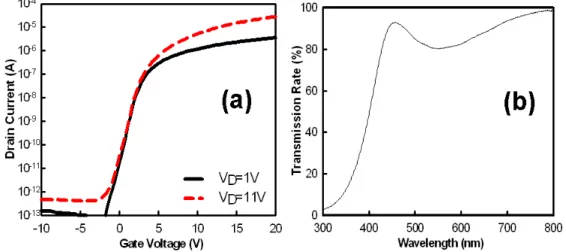
Figure 2 (a) shows the transfer characteristics of the a-IZO TFT biased at different drain voltages (VD). The threshold
voltage (Vth), subthreshold swing (S.S), and effective field mobility extracted at VD=1V are 0.75V, 750 mV/decade, and
44.68 cm2/V.s, respectively. The electrical performance of the a-IZO TFT device is so good that it can be applied for
peripheral circuits in a flat panel display. For the photo-reaction characteristics, the energy band gap of a-IZO film is about 3.05 eV, and theoretically sensitive to the illumination light with the wavelengths shorter than 400 nm. However, the transmission curve measured by UV-visible system presents that a-IZO film seems to have absorption reaction to the
visible light spectra between 450 nm to 700 nm, as shown in Fig. 2 (b). The photosensitivity of a-IZO film to visible light can be attributed to the defects present in the amorphous IZO film prepared by the sputtering process. Also, these defects play the role of electric trap centers and form trap states in the forbidden energy band gap (Eg), enhancing the
optical absorption.
Figure 2 (a) The transfer ID-VG curve of a-IZO TFT measured in initial dark states at VD=1 and 11 V. (b) The
transmission rate with different wavelength lights. It is clearly to found that a-IZO can absorb visible-light under visible light region.
To investigate the photo-sensitivity of the a-IZO based TFT, we used the incandescent lamp as the light source to illuminate the a-IZO TFTs and recorded the ID-VG curves under the initial dark state (referred to as the Initial), instant
light illumination (referred to as the L0) and light illumination for 10 minutes (referred to as the L10). The measurement temperature was well controlled at room temperature. With constant current method to extract the electrical parameter in saturation region, the threshold voltage was 0.22V, -11 V and -11.89V for the measurement conditions of dark state, instant light illumination and 10min-illumination, respectively as shown in Fig. 3 (b). The a-IZO TFT transfer curves were observed shifting in the direction of negative voltage as a result of exposure to light illumination.
Figure 3 (a) The transfer ID-VG curve of a-IZO TFT measured under the initial dark state (referred to as the Initial),
instant light illumination (referred to as the L0) and light illumination for 10 mins (referred to as the L10). (b) The evolution of Vth after light illumination as a function of illumination duration.
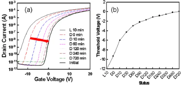
Figure 4 shows the evolution of ID-VG curves after removing light source for the a-IZO TFT devices staying at
the dark. After the 10-min-light-illumination, the a-IZO TFTs which stayed in the dark for various durations from 0 to 720 min were referred to as D0 and D 720. It is clearly observed after removing the light illumination that the transfer curves of the a-IZO TFT shifted in the direction of positive voltage to a limited extent (Vth being -9.1V),
and did not return to the initial dark state immediately. After 720 min period of time, the transfer curve recovered its initial dark state, as shown in the D720 curve of Fig. 4(a). The evolution of Vth as a function of staying duration in
the dark is summarized in Fig. 4(b).
Figure 4 (a) The transfer ID-VG curve of light-illuminated a-IZO TFT after removing light source and then
measured in the black boxes to keep samples from disturbance of ambient environment. The a-IZO TFT devices were laid in a black box for 12 hours. (b) The evolution of threshold voltage of the light-illuminated a-IZO TFT as a function of staying time in the dark, recorded from measuring stage D0 to D720.
Previous studies have reported the physical and chemical absorption reaction of oxygen with TCO films like a-IZO was very slow. In 1977, Y. Shapira et al. have used the proposed theory to explore the relationship between the changes of carrier concentration and time. [11] In the thesis, the rate of change of the conductivity was proportional to the change in the surface density of ionized gas from the ambition environment, and would decrease reciprocally with the square root of stay time (t), as described below.
2 1 −
∝
Δ
t
dt
N
d
(1)where N is excess electron concentration. Although the actual case was not quite the same as the formula Y. Shapira et al. derived, the main point of his studies lay in the influence of surrounding gas and the slow reaction and nonlinear relation with time factors. The physical and chemical absorption of oxygen species from ambient air with ITO-based film can be described further as the reaction Eqns. (2) and (3) as followed. [12][13]
− −
↔
+
2 2e
O
O
(2)
+ −+
↔
O
h
O
2 2(3)
where e− denotes electrons and h+ denotes holes. In this experiment, O
2(gas) was present in the ambient air and was easily
negatively charged (O2(solid)-) by capturing free electrons. An a-IZO TFT is an n-type semiconductor with many electrons.
Chemical reactions will also be equilibrated dynamically in the ambient. This suggests that the reaction equilibrium is disturbed and the net reaction direction moves toward the right side of the reaction equation. Conducting electrons are trapped by O2(g) to form O2-. The resultant buildup of negative space charges easily repels conduction electrons in the
negatively shift while the chemical reaction moves toward the left. Generally, excess electron-hole pairs are generated and contribute to photo leakage current in electronic devices while a typical semiconductor exposes to light illumination. In the n-type a-IZO film, the percentage change of minority-carrier (hole) concentration originating from light illumination becomes more significant than that of majority carrier (electron) in a-IZO film. The variation of hole concentration disturbs initial chemical equilibrium and reacts Eq. (3) shift left while Eq. (2) remains itself, causing the net reaction transferring toward the left. As a result, after light illumination to the a-IZO TFT, the Vth shifts in the
direction of negative voltages as indicated in the curve of L10 of Fig. 3(a).
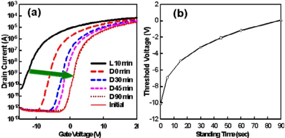
To confirm the validity of the proposed mechanism responsible for the photoreaction behavior, a charge pumping procedure was conducted to disturb the equilibrium of Eqns. (1) and (2) by increasing the electrons in the a-IZO film. We propose a charge pumping method to accumulate electrons in the a-IZO channel. In this work, a 5V voltage of charge pumping was first applied to the gate electrode. The applied gate voltage of 5 V was verified in advance so as not to degrade electrical characteristics of the a-IZO TFT. Compared to the result of no gate bias application (720 min), a period of 90 min was required to return the electrical characteristics of the light illuminated a-IZO TFT to the initial dark state, as shown in Fig. 5(a). The evolution of staying time versus threshold voltages of a-IZO TFT with a pumping voltage of 5V is shown in Fig. 5(b). The speedy recovery of electrical characteristics was attributed to excess electrons accumulated in the a-IZO layer. These electrons were responsible for shifting Eq. (2) toward right. Consequently, the resultant increase of O2- speed up the Vth of the light-illuminated a-IZO TFT positively shifts and return to the initial
dark state, as discussed above. The nearly matching transfer curve between the a-IZO TFT with and the a-IZO TFT without 5 V gate bias also confirms electrical degradation not to occur during the charge pumping process. As mentioned in previous studies on conventional amorphous silicon-based device, small voltage and short time gate voltage bias stress would cause state creation effect, and changed the threshold voltage and subthreshold swing.[14] However, in this work this phenomenon was not been observed. This also indicated the prepared a-IZO TFT devices can exhibit good electrical stability. In this experiment, we also found rapid recovery of the threshold voltage is achieved within a period of 10 min, as the gate pumping voltage increases to 35 V. It can also be well explained by the proposed model in Eqns. (2) and (3). The recovery property results of high pumping voltage with short time period potentially create the application for photosensor devices.
Figure 5 (a) Transfer characteristics of the 10-min-light-illuminated a-IZO TFT, which was gate-biased at a DC voltage of 5V for 5, 15, 30, 45, 60, and 90 min, respectively. It only took 90 min to return to initial dark state. (b) The extracted threshold voltage (Vth) from Fig. 5 (a) as a function of standing time in the black box, while a
pumping voltage of 5V was applied to the gate electrode of a-IZO TFT device.
The schematic circuit and timing chart for the proposed photosensor technology are shown in Fig. 6. TFT 1 is the main a-IZO TFT device to sense the light intensity and then converts it to current signal. TFT 2 is a switch device to be turned on/off by the sequential pulse signals. G1[1] and G2[1] are the pulse signals in first row. In
the reset pulse period, G1[1] to G1[n] give higher positive pulse to reset the TFT 1. At the scan pulse period, G1[1] and G2[1] supply synchronic timing pulse to read the current signal in each row. Eventually, the current signals is inputted to an analog-to-digital converter (ADC) block for logic calculation. In this case, the G1[1] can be set at -2V. While in the dark (e.g. Vth = 0.25 V), the applied VGS of -2V maintains the a-IZO TFT cutoff,
resulting in an output voltage equal to the power supply voltage (depend on DC power in Fig. 6 (a)). The output power (Poutput) is equal to ID×VDS=0. In the other hand, after light exposure, the Vth negatively shift, causing the
applied VGS of -2V to turn the a-IZO TFT on and pull the output voltage close to zero. This indicates the power
consumption of light sensing element will be low and potentially realize an array circuit form for the photosensor technology. The proposed charge pumping method can be applied to rapidly refresh the sensing element which consists of an a-IZO TFT, and to repeat the cycle.
Fig. 6 (a) The proposed photo-sensor circuits. (b) The synchronic timing pulse to read the current signal in each row
4. CONCLUSION
In short, we investigated the photoreaction of a-IZO TFTs. Experimental results have shown the Vth shift occurred
on the a-IZO TFT after visible light illumination. The mechanism responsible for photoreaction behavior can be explained by the dynamic equilibrium between O2(g) and O2- in the a-IZO layer. The recoverability of electrical
characteristics to the initial state is rather slow. The physical mechanism for the photoreaction reversibility has been investigated and confirmed experimentally through an external gate voltage triggering. With a charge pumping method, the recoverability of electrical characteristic is speeded up remarkably. A rapid recovery of the threshold voltage even can be achieved within a period of 10 minutes, as the pumping voltage increases up to 35V. The knowledge of physical mechanisms for the photoreaction behavior of a-IZO TFT will be potentially beneficial for photosensor technology applications.
ACKNOWLEDGMENT
The authors would like to thank the National Science Council of the Republic of China, Taiwan, for financially supporting this research under Contract Nos. NSC 96-2221-E-009-130-MY3.
REFERENCES
[1] N. L. Dehuff, E. S. Kettenring, D. Hong, H. Q. Chiang, J. F. Wager, R. L. Hoffman, C. H. Park, and D. A. Keszler,
J. Appl. Phys., 97, 064505 (2005)
[2] H. Q. Chiang, J. F. Wager, R. L. Hoffman, J. Jeong, and D. A. Keszler, Appl. Phys. Lett., 86, 013503 (2005) [3] P. F. Carcia, R. S. McLean, M. H. Reilly, and G. Nunes, Jr, Appl. Phys. Lett, 82, 1117 (2003)
[4] J. H. Choi, I. S. Joo, K. H. Chung, U.S patent, US 7218048 B2 (2007) [5] P. T. Liu, Y. T. Chou, and L. F. Teng, Appl. Phys. Lett. 94, 242101 (2009)
[6] K. Nomura, H. Ohta1, A. Takagi, T. Kamiya, M. Hirano, H. Hosono, NATURE, pp. 488-492 (2004)
[7] H. Yabuta, M. Sano, K. Abe, T. Aiba, T. Den, H. Kumom, K. Nomura, T. Kamiya, and H. Hosono, Appl. Phys. Lett.
89, 112123 (2006)
[8] P. T. Liu, Y. T. Chou, and L. F. Teng, Appl. Phys. Lett., 95, 233504 (2009)
[9] K. Vanheusden, C. H. Seager, W. L. Warren, D. R. Tallant, and J. A. Voigt, Appl. Phys. Lett. 68, 403 (1996) [10] Q. H. Li, T. Gao, Y. G. Wang, and T. H. Wang, Appl. Phys. Lett., 86, 123117 (2005)
[11] Y. Shapira, R.B McQuistan, and David Lichtman, Physical Review B, 15, No. 4 (1977)
[12] Yasutaka Takahashi, Masaaki Kananori, and Akiko, Kondon, Jpn. J. Appl. Phys., 33, 6611 (1994) [13] R. Keezer, J. Mudar, and D. E. Brown, J. Appl. Phys, 35, 1868 (1964).