A
Portable
All-Digital Pulsewidth Control Loop
for SOC Applications
WeiWang, I-Chyn Wey, Chia-Tsun Wu, andAn-Yeu(Andy) Wu
Graduate Institute of Electronics
Engineering,
and
Department of Electrical
Engineering,
National
Taiwan
University,
Taipei 106,
Taiwan,
R.O.C.
Abstract A cell-based all-digital PWCL is presented in this blocks and custom layout of the ADPWCL are redesigned paper. To improve design effort as well as facilitate system- for each new technology. Thus, efforts at physical design
level integration, the new design can be developed in level remain unsolved.
hardware description language(HDL) and implementedwith In order to provide fast turnaround time, a PWCL is
standard-cell libraries, therefore, easily portable between desirable to be globally flexible to fit various system technologies. In addition, a high-resolution architecture is specifications, such as acquisition range, technology designed to enhance pulsewidth precision. For different changes, andintegrated simulations, etc.
Thus,
a cell-basedrequirements of applications, the characteristic of scalable all-digital solution for PWCL with high-resolution and modulating range allows hardware decision in early stage. scalable-acquisition-range is presented in this paper. The Theproposed methodology hasbeen provenatUMC0.18um new ADPWCL can be described by Verilog HDL and CMOS technology. When operated at 350 MHz, the pulse implemented through synthesis and layout CAD tools. widthacquisition rangesfrom 10% to 85% with 0.9%steps. Based on scalable function blocks, it allows architecture I. INTRODUCTION decision in early stage. Also, due to cell-based feature, new
In CMO crcutesinsgratattntonsmutbpid ADPWCL can be incorporated into HDL-level simulation In CMOS circuit designs, great attentions must be paid and system evaluation. A prototype design is realized at toclock quality,includingfrequency, distribution, phase and
UMC
0.18um
technology. When operated at 350MHz,
the duty cycle. Currently,phase-locked
loop (PLL) ordelay-
ADPWCL gives modulation range from10%
to85%
with locked loop (DLL) is widely utilized for clock circuitry.0.90/O
acquisition steps and simulationRM\S
jitter of 25ps.Precise duty cycles are often required to fit demands in
modern high-speed and low-power circuit designs. Even II. CELL-BASED ALL-DIGITAL PWCL ARCHITECTURE
though PLL and DLL can reach
frequency multiplication
and phasealignment, they cannot offer desired
duty
cycles
DPWM(scalable)of clock signal. Pulsewidth control
loops
(PWCLs) [1]-[4]
Input Clock, Clock Buffer OutputClock,can be used to overcome this
problem.
Figure
1 shows a _conventionalPWCLcircuit.
...
00
FeedbackControl
DPWC|
Pseudo Odd-Stage Clock Diiver PWA,DPeS,FT
CKin Reference~~~~~Cou
.LH,.1
Cl.Dhded
CZocl:LCg
~~~~~~~~~~~~~~~~Progra
Cod,PC
S XW
~~~~~~~~~~~~~~Figure
2. Proposed portable ADPWCL.CKIn Loo FitrC
aaor/Dgt,
m...
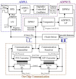
Ablock
diagram of portable ADPWCL is shown incomparator Figure 2. Overall system is decomposed into five main Figure 1 Atypical
PWCL
circuit function blocks: 1) Clock Buffer providing suitable driving strengths for application circuits, 2) Digital Pulsewidth The PWCLs in [1][2]were
proposed to precisely adjustConverter
(DPWC) cyclically converting the pulsewidth of theoutput duty cycle of the multistage driver. Most PWCLs CLKout into binary digits, 3) Comparator performing [1]-[3] are realized by analog approaches at present. pulsewidth comparison and lock detection, 4) Loop FilterHowever,
asdiscussions
in [2]extensive
circuit simulations utilized to reduce the noise coming from the environment,areusually
performed
todetermine loop gain and loop filter. and generate digital control codes of feedback control, and 5) Also, an analog PWCL usually takes alongstransientttimettoDigital
Pulsewidth
Modulator (DPWM) responding forconverge. Recently, a robust all-digital PWCL (ADPWCL) modulating pulsewidth. [4] has been
introduced,
where thearchitecture
isconstructed with digital circuits. However, specific circuit
Due to physical constrains of setup/hold time, the power consumptions because redundant propagated clocks
dividerMis usedto slow down target frequencyaswell as are nowgated and saved withinnewdelaycell.
allocate timing for critical path of loop filter. Based onthe To evaluate performances, a prototype 32-stage DPWC
control codes fromloop filter, theDPWMgives the function is realized at UMC 0.18um 1P6M CMOS technology. of modulating pulsewidth with digital techniques. The Compared with conventional design, the new DPWC
feedback loopoperatescontinuously untilcomparator enters improves operating frequency from 350 MHz to 1GHz.
locked state, namely the DPWC quantization digits (QD) According to conversions of different duty cycle, power match the external program code. The ADPWCL can savings are listed in tableI.
generatedesiredpulsewidth for demands of applications.
QD[O] QD[1] QD[2] QD[3] QD[30] QD[31]
A.
Digital
Pulse Width Converter(DPWC)
Rn Rn Rn n RDQDQD Q D Q D Q D Q
To measure the continuous clock
pulsewidth
indigital
CKinway, thedesign concept oftime-to-digital converter [5] can
be cited for purpose. A transformed architecture [4] has --- D..
been introducedto convertpulsewidth into binary digits, as
CKin
tTT
shown in figure 3. The incoming clock signal propagates D,through the buffer chaintobecomeaseries ofdelayed clock D2K
signals.
Thedelayed
clocks areutilized totrigger
the DFFs D a_ r IN OUTsuccessively, and measure the
pulsewidth.
The ratio of 4 - 4t-IL-: consecutive "1" and total word length represents the duty 3cycle.
Thus,
a continuous clockpulsewidth canbe digitallyquantizedinto n-bit word. Figure4. ModifiedDPWCarchitecture.
However, the long critical path of conventional DPWC TABLEI. COMPARISIONS OF POWER COMSUMPTION
is quite long and therefore limits operating frequency. While
thepropagated clocks areused for quantization, great deals
TypCcl (@0)
75% 50%25%
ofpowerdissipationscanbe contributed. Typical(uW) 1602 1872 2016
Proposed (uW) 1058 774 503
1/8 cycle PowerSaving 34% 59% 75%
B.
Digital
Pulse Width Modulator(DPWM)
QDJ0:311 1 1 I 0 0 0 0 0 0 0 0 0 0 0 0 0 0 0 0 0 0 0 0 0 0 0 0 0 0 0 0
A pulsewidth modulator gives the function of reshaping
QD[O1QD[1J QD[21 QD[31 QD[301 QD[311
CK... clockwaveform.
Analog
modulators[I]-[3]
anddigital
oneQ D Q D Q D Q D Q D Q
[4]
have been utilized to modulatepulsewidth.
However,
> >
>L >Ll
r- --< rLspecific-purpose
circuitdesigns
and customlayouts
arestill.~
D D, L ,---- required. It still takes design efforts during technology_----'-'''-''''''''''-'''-''''''-'''-'''''t'' ..'' m igrations.
ck > Therefore, wehave three design goals in developing a
DI: ... !!IN portableclock modulator. First, the portable
DPWM
shouldD2
,I* . TypicalBuffer be suitable for cell-based flow andcapable
for variouscell-D4:: |: | | | | 1___l 1
1,Ilibraries.
Second, scalability of acquisition range is desiredD_____!__!__!_!!
!
FT forspecification changes.
Third,
pulsewidth
deviation'i .321. . .. ' ' ' ' >I ' 'should be carefully reduced to meet demands of advanced
Figure 3. Conventional DPWC architecture.
applications.
Thus,
ourproposed
DPWM isdecomposed
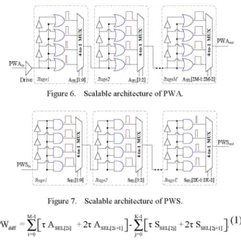
into scalable pulsewidth amplifier (PWA), pulsewidth Therefore, a modified DPWC is designed to solve the shrinker(PWS) and fine-tune unit (FTU). ThePWSreduces issues. Thepulsewidth of clock decides duty cycle, and the the
pulsewidth according
todigital
control codes. On the pulsewidth conversion is processed between clock's rising contrary, thePWAamplifies
thepulsewidth.
FTUprovides
and falling edges. Thus, the propagated clocks after falling fine
acquisition
stepofpulsewidth,
asshowninfigure
5.edge could be expectably avoided. As common cell
constructions, a bufferusually consists oftwo inverters. In PIAS CoarseStep
(1
LOps) PVVA CoarseStep(120ps) orderto saveredundantpropagated clocks, the first inverter Iis replaced by aNAND and the input clock is transplanted fromDFFtodelay cellasshowninfigure4.
TheDPWC operation completes just intime after clock F S
falling edge; therefore, the critical path iS significantly
I reduced. Also, since the setup-time physical constrain ofDFF iS resolved, the dead
zone,non-ideal conversion
OfIiue5
uswdh custoso PMnarrow pulse, is reduced. Moreover, the new DPWC reduces
Toillustrate the detail
circuit,
the PWA consists of PWA Inaddition,
it is essential tofixrising edge
of eachstage
stages
asfigure
6. Each of PWAstage
provides
4paths
for in DPWM\during
control code switches. The characteristicsignal propagation. Passing through
the lowestpath
of each stabilizesphase-locking
in PLL and allows furtherstage,
thepulse
width of clock is remained. If clocksignal
cooperation
of PLL in later section.passes
through
an upperpath,
thepulsewidth
isamplified,
Aprototype
modulator,
consisting
of five PWA/PWSnamely,
thepulsewidth
difference ofadjacent paths
inthesame stageis equivalentto one buffer delay z. Also, amd
stages
andoneFTUstage,
provides
(5*3±5*3)*3
acquisition
at
reducing pulsewidth,
the PWScomposed
of PWSstages
stps.SIEsmltoso
puswdhm
ultositois dpicedfgur 7.Thecascdedpulewithn ncrase cases
(PWA, PWS)
aregiven
infigure
9. The robust andisWdepictnb
eied
figure7.Thincacaedepulsewidthe
incrase
linear characteristic ofDPWM\
architecture allowssimple
ofPWdAf
cabeSdscribedsiAEq.(1, whsepresMKaen
theotrotl
formulation ofpulsewidth.
In addition to coarsesteps
ofcofesPWAe/pWSctagsiSE,adeSLrersnttecoto
hundredpicoseconds,
FTUprovides
fine
resolution of3Ops
codes,respectively.
~~~~~~~~as
figure
10.Compared
with traditionaldesigns
[I]-[4],
theproposed
11 ~~ EL ~~ DPWM can be constructed with commonlogic
cells,
I PWA therefore
easily
transferr
ed between cell-libraries. Theconsistence allows the architecture very suitable for
PWA,,,~ ~~~ ~ ~ ~
Nextending acquisition
range andenhancing
resolution. Theuniversal architecture
gives design flexibility
forapplication
Drive ---O /~ e\A--[---2----M--]specification
and..
hardware decision inearly
stage.
Figure6. Scalable architecture of PWA. PAP,I,. Width
M.d,Iati-~
PSP,.Witdlt-4000 2200 3600 16~~~~~~~--- 00 ~~ pws~~~~~~, 3~~~4000 -=1--00----7K Y1~~~~~~~~~~~~~~~~~~~~~~~~~~~~~
~~~~3200--- ---
2C0 ---2400 ---00--lp2400- 400---Figure 7. Scalablearchitecture ofPWS. ~~~~~~~~~~~~~~~~~~320--- 0
M-l K-i (1) Figure 9. Post-layout Simulations of PWA andPWS.~~~~~~~~~~~~~~~~~~~~~~~20
---PWdfff~~~~ [~~ A~~2~~1 +4xAEL21 1-4 xSE[i xSE[i1
i=O ~ ~ ~ ~ ~ ~ ~~~~~~~~~~~~~~~~~~~~~~~~~~~~~~~~~~~~~30 10 ---I
A nwi
meho8o0mpovnrsouto-i-poosd-o
reducing pulsewidth deviations. The main idea is using the~~~~~~~~~~~~~~~~~~~~~~~~~00---
---the FTU providesprecise acquisition step r. Eq. (2) e(ns)~~~~~~~~~~~~~~~~~~~~~~~55~s0 1 i
represents thepFiulsewidt incrlbeascieo tu.rTe equialece Fgur
10.,o
SmltonsadPcaraceritics
of FTacquisitionurrangeosoflDPWMt
ismexpressedf
inAEq.d(3).
newmethod
oAnmpintegrationutsystem
ispodesigned-to--ve---the
8,
a few buffercapacitancethesscaabilityepoblemscasedtby
poularabusbased Sowireoad.Figuere8
Achpaitenctue
lofd
Fine-unes
Unit.isnlo
the
---key
techolog
to---
overcome-- the--wire-complexity--
to
usage of tresinglEde-hs pus-rgedbad sif
theFT
povdeWM
pWeis
acq +FstUotpr
q(3)
reitrTwihrqirsacocminlwihnro
duty-repreents
hepuseouth
incre oiffifFU
cycle,valnc
Figunsbelo.SiuaonadchrtesisofFUThe ADPWCL
dynamically
controls and modulates IV. COMPARISIONS OF PWCL DESIGNSpulsewidth
while ADPLLperforms operations
ofphase
__________aligniment
andfrequency synthesis.
With thecooperation
of Design JSSCO2 APASICISCAS05
OursADPWCL and
ADPLL,
theoutput
clock can fulfill the Prcs[21
02131 141 ____demands for desired clock of
applications.
Theprototype
Process___ 0.35um 0.l18um 0.25um 0.l18umintegration design
is verified and realized at LUM\C 0.18um Architecture Analog Analog Alldigital AlldigitalI1P6MCMOStechnologyasfigure 12. Technique Custom Custom Custom Cell-Based
ADPLL ADPWCL Programmable N Y Y - Y
I--- Portable N N N Y
ICKR. ADL 9iitly Acquistion 5000 20 5Oo 20 80o 0~8
PFD Controlled DPWM I ~~~~~~
~~~~~~~~~~~~~~~~~~~~~~~Range
-(0.8GHz)
(0.4GHz) (0.3GHz)-(0.35GHz)
phas~
---O-cillator-
[l~1JiResolution 0.25 ns/V 500 1000 0.9001/N iI DPWC Comparator LF V. CONCLUSION
N[70
~
~
~
~
~ ~ ~
ITo
meet the demands for fast turnaround time of SoCM1ItqpInUi gramCode[310]
I-
--Mli-cton
CnerinIapplications,
a portableall-digital
PWCLdesign
isPClockCKjp PuswdhMdlto
developed.
The modified DPWCpresents
low-power
and LIL FLIL~~~~~~optimized-latency
operations.
Ahigh-resolution
DPWM\ is Communication~~~~Commucain
firstproposed
to enhancepulsewidth precision.
With Cnimucation scalable circuit blocks andsynthesizable loop
controller,
TransmfterReceiver
designers
candevelop
ADPWCLinVerilog
andsave effortsItClk(Trasit) intClk(Recive)
significantly.
Wvhen
operated
at350MH-z,
thepulsewidth
P/SConverter Tr/P"O
Covrecquisition
rangeis from100o
to850o
with 0.9 00steps.
ThevvvvvviI
ADPWCLdesign
can beefficiently incorporated
into Tx DtaCntro P- atamodern SoCdeinflow du oitsIPbsdfaueTExtClokk ExtClokk2 AcKNoWLEDGMENT
On-Chip
Conmmuniato
The authors thankChip
Implementation
Center (CIC)Figure11. On-chipserial communicationsystem. for CAD toolsupportsand technical discussions. REFERENCES
[1] Fenghao Mu; Svensson, C,"Pulsewidth ControlLoopinHigh-Speed
CMOSClockBuffers,"IEEEJournalofSolid StateCircuits,vol. 35,
___
~~~~~~~~~~~~pp.
134-141,Feb. 2000.tal
~~~~~~[2]
Po-Hui Yang and Jinn-Shyan Wang, "Low-Voltage PulsewidthL ~~~~~~~~~ControlLoops for SOC Applications,"IEEEJournalofSolid-State
Circuits,vol.37,pp. 1348-1351,Oct. 2002.
[3] Kuo-Hsing Cheng, Chia-WeiSu,Chen-LungWu ,andYu-Lung Lo,
~Generator-
"A Phase-Locked PulseWidth Control Loop with ProgrammableDuty Cycle," IEEEAsia-Pacific Conference on Advanced System Integrated Circuits,pp.84-87,Aug.2004.
[4] Yi-Ming Wang, Chang-Fen Hu,Yi-Jen Chen andJinn-Shyan Wang,
"An All-Digital Pulsewidth Control Loop," IEEE International
Figurelayotof the12.Chip OC
system.Symposium
onCircuitsandSystems, pp.1258-1261,May2005. Figure12.Chiplayot of the 0C system.[5] Levine, P.M.; Roberts, G.W, "A calibration technique for ahigh-resolution flash time-to-digital converter," IEEE International
Figure
13 shows the ADPWCL converges and enters SymposiumonCircuitsandSystems,vol. 1,pp.253-256,May2004. into lockedstateaccordingtodifferentprogram codes at350 [6] I-ChynWey; Lung-Hao Chang; You-Gang Chen; Shih-Hung Chang; MHzwith SPICEsimulations. An-Yeu Wu, "A High-Speed Scalable Shift-Register BasedOn-Chip Serial Communication Design for SoC Applications" IEEE International Symposium on Circuits andSystems, pp.1074-lO77,
-~10% May2005.
Time(ns)