國 立 交 通 大 學
電子工程學系 電子研究所碩士班
碩 士 論 文
以雜號干擾最小化為目標並符合延遲條件之技術映射
Technology Mapping Algorithm Targeting Crosstalk
Minimization under Specified Delay Constraints
研 究 生:范芳瑜
指導教授:陳宏明 博士
以雜號干擾最小化為目標並符合延遲條件之技術映射
Technology Mapping Algorithm Targeting Crosstalk
Minimization under Specified Delay Constraints
研 究 生:范芳瑜 Student: Fang-Yu Fan
指導教授:陳宏明 博士 Advisor: Dr. Hung-Ming Chen
國 立 交 通 大 學
電子工程學系 電子研究所碩士班
碩 士 論 文
A Thesis
Submitted to Department of Electronics Engineering & Institute of Electronics College of Electrical and Computer Engineering
National Chiao Tung University in partial Fulfillment of the Requirements
for the Degree of Master
in
Electronics Engineering July 2008
Hsinchu, Taiwan, Republic of China
以雜號干擾最小化為目標並符合延遲條件之技術映射
學生:范芳瑜 指導教授:陳宏明 博士 國立交通大學 電子工程學系 電子研究所 碩士班摘 要
在現今的超大型積體電路的設計中,隨之成長的雜訊干擾現象而造成
晶片失敗或良率降低,已變成很重要的課題。在本篇論文中,我們提
出了在技術映射階段,就可減少雜訊干擾並符合延遲條件的演算法。
在技術映射的比對階段,此演算法採用了動態規劃架構,並且為了能
機率性地估量通道的佔用,所以決定了所有配對的輸入端的繞線,這
些繞線將被儲存成虛擬的繞線地圖,以期在覆蓋階段能夠計算雜訊干
擾;而在覆蓋階段,將會選擇雜訊干擾最小且符合延遲條件的配對來
取代延遲最小的配對。根據以聯電 90 奈米製程為技術資料庫而進行
對標準測試電路的模擬實驗中,在對傳統的延遲最佳化之技術映射比
較下,顯示了我們的演算法可以有效的減少雜訊干擾,改進平均值達
到百分之二十五。
iTehchnology Mapping Algorithm Targeting Crosstalk Minimization
under Specified Delay Constraints
Student: Fang-Yu Fan Advisor: Prof. Hung-Ming Chen Department of Electronics Engineering
Institute of Electronics National Chiao Tung University
ABSTRACT
In today’s VLSI designs, the growing of crosstalk effects causing chips to fail or suffer from low yields has become the important issue. In this thesis, we propose a technology mapping algorithm that can reduce the crosstalk noise while meeting delay constraints. The algorithm employing a dynamic programming framework in the matching phase determines the routing of fanin nets for all the matches to estimate the track utilization in probability. These routings are stored as virtual routing maps to compute the crosstalk noise during the covering phase, which will select the crosstalk-optimal solutions satisfying the delay constraints rather than the delay-optimal ones by slack caculation. Experimental results on benchmark circuits in UMC 90 nm process show that the algorithm is effective to improve the crosstalk by 25% on average, as compared to the conventional delay-oriented technology mapping.
誌 謝
本書得以完成,必須要感謝許多人。 對所有幫助、鼓勵我的教授、家人、同學以及朋友致上深深的謝意! 感謝指導教授陳宏明博士,教授耐心協助及適時給予意見,讓我能夠順利完成畢 業論文研究,還有在生活上,感謝教授的幫助。 感謝蔡孟家同學,在我研究論文過程中,遇到困難及問題時,和我一起討論,提 出個人的看法,讓我獲得許多寶貴的參考意見。 感謝施盈安學長,熱心指導我關於實驗軟體上的使用,還有幫助我解決實驗上的 問題,讓我得以順利完成實驗。 感謝李仁傑學長,不只在課業、研究,還有生活上所給予的意見及經驗,讓我獲 益良多。 感謝睿斌和篤雄同學,一起陪我度過研究所兩年的學習日子,在課業上、研究上 互相抵礪。 感謝實驗室同學,在課業上及生活中互相鼓勵、研究及幫忙!Contents
1 Introduction 1
1.1 Our Contributions . . . 3
1.2 Organization of This Thesis . . . 4
2 Preliminaries 5 2.1 Technology Mapping with Layout Information . . . 5
2.2 Crosstalk Model . . . 8
2.3 Problem Formulation . . . 10
3 Algorithm for Crosstalk-Aware Technology Mapping under Delay Constraints 11 3.1 Our Methodology . . . 11
3.2 Virtual Layout Generation during the Matching Phase . . . 13
3.2.1 Bottom-up Virtual Routing Map Construction . . . 14
3.2.2 Handling Multiple Fanouts . . . 15
3.2.3 Comparison with Recent Works in Technology Mapping . . . . 15
3.3 Crosstalk Minimization under Delay Constraints during the Covering Phase . . . 16
3.3.1 Algorithm for the Crosstalk-Aware Covering . . . 19 3.3.2 Procedure for Obtaining Crosstalk-Optimal Match under Slack
constraints . . . 21 3.3.3 Time Complexity of Our Approach . . . 23
4 Experimental Results 24
4.1 Experimental Setup . . . 24 4.2 Experimental Results . . . 26
5 Conclusions 30
List of Figures
2.1 The expression of load-delay curve. (a)A load-based delay model for an inverter in typical stardard cells. (b)An example of the load-delay curve stored in each node during the matching phase. . . 6 2.2 The delay model representing in RC tree. (a)An example of a
com-binational circuit. (b)The corresponding RC model, where a gate is modeled in the loading for its inputs and the driver for its outputs; a wire is represented by the π model. . . . 7 2.3 The crosstalk effects on a circuit. (a)An example of the coupling
effect from the switch of a signal in a combinational circuit. (b)The ideal signal transmission without the coupling effect on the victim net (c)The real signal transmission coupling by a switch from high to low of the signal s1 on the victim net. . . 9 3.1 The overview of our methodology in predicting layout information.
(a)A desgin flow divided into five stages from the RTL design to the physical noise analysis. (b)The corresponding process for each phase to predict the layout information in technology mapping. . . 12 3.2 The overall flow of our crosstalk-aware technology mapping. . . 13
3.3 The explanation of pre-placement and pre-routing in the matching phase. (a) An example of a matched gate with its fanins’ and fanouts’ rectangles, the new position of this gate is the gravity center of these rectangles [11]. (b) The corresponding virtual routing map in bins for the gate and its fanins. The rectangles in dotted line are the routing windows for L- or Z- shape routing patterns. Our quick router would choose the appropriate patterns with least congestion. . . 14 3.4 The coupling capacitance of a unit segment on net 2 is contributed
by net 1, so the routing for net 1 and net 2 has to be determined. . . 16 3.5 Six configuraions of adjacent nets. The bold net is the net under
consideration; dotted nets represent empty tracks. . . 16 3.6 An example of a routing map and its corresponding RC tree. (a) An
example of the routing map and the thicker net is under consideration. (b) The corresponding coupling capacitance and wire resistances tree for the thicker net in horizontal direction. . . 18 4.1 Our experimental flow for the conventional and crosstalk-aware
map-ping. . . 25 4.2 The crosstalk improvement results comparing between the
conven-tional delay-oriented mapping (SIS) and Our crosstalk-aware map-ping (SIS Xtalk). All the data of ours are normalizing to SIS. . . . 29
List of Tables
4.1 The comparison of area and delay between the conventional delay-oriented mapping and our crosstalk-aware mapping. The increase in area and delay shown in percentage is the tradeoff of the improvement in crosstalk for our crosstalk-aware mapping. . . 27 4.2 The comparison of crosstalk noise and run-time between the
con-ventional delay-oriented mapping and our crosstalk-aware mapping. The crosstalk ratio of number of the receiver peak net to number of the total net is shown in percentage. The crosstalk noise for our crosstalk-aware mapping exactly improves up to 25% by experiments. 27
Chapter 1
Introduction
In the deep sub-micron era of the VLSI fabrication, the numbers of devices have increased by following Moores law—doubling every two years, and the numbers of wires have grown at the same rate simultaneously. As a result, the interconnect wires become taller and thinner with smaller spacing and higher sidewalls almost like parallel plate capacitors, thus raising the coupling capacitance between wires even more than 50 percent of the total wire capacitance. The growing of coupling effects not only increases signal delays but also decreases signal integrity in view of the transmission line behavior. This phenomenon is called crosstalk , causing chips to fail, under-perform or to suffer from low yields [1].
Due to the large influence of crosstalk, many previous works made efforts in solving crosstalk problems in different design flow stage. Generally, at the post-routing stage, crosstalk reduction could adopt transistor sizing, gate sizing or wire sizing for the accurate noise analysis based on the RC extraction of layout [2, 3, 4, 5, 6]. However, the flexibility of adjusting netlists might not be enough to fix hundreds or even thousands of noise problems, so eventually those unsolved noise problems would only rely on the rip-up and reroute step. The design would probably suffer in numbers of iterations in the post-routing stage. Consequently, numerous works have focused on crosstalk avoidance at routing or placement stage. [7] established a
crosstalk model into a global routing problem solving by Lagrangian relaxation, and then [8] provided a crosstalk-constrained maze routings based on this model. [9] proposed a crosstalk-aware placement to estimate crosstalk noise by a probabilistic model. Similarly, [10] worked on placement stage to reduce crosstalk more effectively, adopting more accurate noise model to generate a noise map in crosstalk analysis.
Based on these previous works on crosstalk avoidance, we attempt to consider crosstalk at the earlier stage in the design flow—at the synthesis stage, due to the reason that logic synthesis can offer a larger degree of freedom to modify the com-positions of circuits, not just the placement or the routing. Therefore, handling crosstalk problem during synthesis can not only remedy the restriction of flexibility in adjusting circuits but also reduce the numbers of design iterations more success-fully. In the synthesis process, technology mapping, which assigns Boolean functions to gates from the custom library, is powerful to decide interconnects and then to impact on crosstalk effects apparently. Nevertheless, the difficulties of this idea re-main in how to estimate physical information accurately and to analyze the crosstalk noise efficiently, since technology mapping operates at a higher level of abstraction than the placement and routing stages.
In fact, technology mapping algorithms considering physical information, such as placement and routing congestion, are not new. For example, [11] presented a technology mapper integrated with a companion placement to consider layout area and wire delay. Recently, there has been growing interest in technology mapping targeting routing congestion. [12] utilized mutual contraction and net range to pre-dict wire length, thus minimizing wire cost and reducing congestion. The work in [13] employed predictive probabilistic congestion estimates to locate congestion-optimal matches; likewise, [14] also used probabilistic congestion maps to guide its technology mapping algorithm avoiding congestion.
1.1
Our Contributions
In this thesis, we develop a crosstalk-aware technology mapping which is able to reduce the number of noise failure nets effectively at post-routing noise analysis. Our main contributions include:
• During the synthesis process, the available physical information from
pre-placement and pre-routing is utilized to construct a reliable model in cal-culating crosstalk noise. As revealed by the experimental results, the number of crosstalk nets above the noise threshold in noise analysis of the commercial tool, Cadence SoC encounter [15], will be indeed decreased if the circuit is adopted crosstalk-aware technology mapping.
• For all delay-optimal matches, a matching procedure is proposed to
gener-ate two-dimensional coupling capacitance map which is available to predict crosstalk based on the information of pre-placement and pre-routing. Further-more, this method in constructing coupling capacitance map is easily expanded to other physical properties, such as power density or temperature maps.
• In the covering phase, we provide an explicit approach in tradeoff between
crosstalk issues and timing constraints. We also formulate the cost function that is sensitive to congestion( corresponding to the total track overflow [14]) and crosstalk( corresponding to the coupling capacitance map from the match-ing phase) of each match. This procedure of covermatch-ing is not only suitable to satisfy delay but also easy to extend other traditional objectives like area and power; moreover, it can consider several different factors at the same time. The experimental results show that the ISCAS’85 benchmark suite can be improved 25% in crosstalk noise on average.
1.2
Organization of This Thesis
The rest of this paper is organized as follows. Chapter 2 introduces the background of technology mapping and crosstalk model. Then, we also describe the problem formulation in the same chapter. In Chapter 3, we describe the overall methodol-ogy of our crosstalk-aware technolmethodol-ogy mapping separated into the matching phase and covering phase. The experimental results are illustrated in Chapter 4 and the conclusion with future work is presented in Chapter 5.
Chapter 2
Preliminaries
In this chapter, we briefly review the techniques of technology mapping with layout information. Next, the reliable crosstalk model adopted in our technology mapping is introduced. Finally, the problem formulation is illustrated.
2.1
Technology Mapping with Layout
Information
The traditional technology mapping [16] is usually preceded by a decomposition procedure, in which the abstract network is translated into primitive gates, such as 2-input NAND gates and invertors. After that, the mapping procedures in the structural approach typically use a dynamic programming that involves two phases, referred to as the matching phase and the covering phase. In the matching phase, the circuit translated into graphs representation, also called subject graphs, will be compared to pattern graphs, which are associated with the library elements, by the tree-based matching method 1. During a topological traversal of the network, all mapping solutions will be generated by recursive visiting. Next, in the covering phase, a mapped network is built by making a decision from these candidates of matches during a reverse topological traversal.
1The tree-based matching is performed by matching the root of the pattern tree to a vertex of
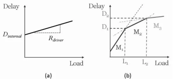
Figure 2.1: The expression of load-delay curve. (a)A load-based delay model for an inverter in typical stardard cells. (b)An example of the load-delay curve stored in each node during the matching phase.
To denote the timing issue, the delay model employed in technology mapping is usually one of the following two classes: load- or gain-based. In this thesis, we only consider load-based delay model, as it is easily extended to gain-based in our algorithm. The load-based delay model [14] is shown in Figure 2.1(a) for a typical standard cell. It shows that the gate delay is directly proportional to the load of the output; therefore the slope of the straight line indicates the effective driver resistance. The delay oriented technology mapping involves storing piece-wise linear load-delay curves during the matching phase, as revealed by Figure 2.1(b), to represent the delay-optimal matches for each load range( called non-inferior matches). Since the output load of each node in the circuit is unknown in the matching phase, the load-delay curve at each node contains these non-inferior matches. Hence, during the covering phase, while loads are known, delay-optimal matches are only chosen from the curves. SIS [17] uses this scheme for its delay oriented mapper, and we employ the same framework for our crosstalk-aware technology mapping.
In order to estimate wire load and wire delay, it is also required to employ a companion placement for the subject graph to estimate wire lengths. It has been
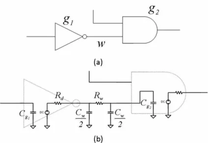
Figure 2.2: The delay model representing in RC tree. (a)An example of a combi-national circuit. (b)The corresponding RC model, where a gate is modeled in the loading for its inputs and the driver for its outputs; a wire is represented by the π model.
already used by previous technology mapping or physical synthesis [11, 12, 13, 14, 18]. Here we use the same concept as [11] to determine the relative locations of matches and calculate the wire lengths; in addition, the wire model [19] based on Elmore delay, RC π model, is exploited in estimating the wire load and wire delay. For example, as can be seen in Figure 2.2(a), gate g1 drives gate g2through a wire w, and the connection of the circuit translated in RC model is shown in Figure 2.2(b). The delay from the input of gate g1 to the input of gate g2 is stated in the following equation:
Delay = Dg1 + Dw (2.1)
where Dg1 and Dw are the delay of gate g1 and wire w. From Figure 2.2(b), Dg1
and Dw can be given by
Dg1 = Dinternal+ Rd× (Cw+ Cg2) (2.2) Dw = Rw×
Cw
where Dinternal is the internal delay of gate g1; Rd is the effective resistance of gate
g1; Cw is the capacitance of wire w; Cg2 is the input capacitance of gate g2, and Rw
is the resistance of wire w.
Normally, the locations of nodes from a companion placement are placed on a virtual layout divided into bins. Each bin contains a limited number of horizontal and vertical tracks. In this thesis, we used the same definition of the track overflow as [14], shown as follows:
DEFINITION: The horizontal (vertical) track overflow for a given bin (T binh(v)),
is defined as the difference between the number of horizontal (vertical) tracks required to route the nets through the bin and the available number of horizontal (vertical) tracks.
From this definition, the total track overflow can be defined as
OF = X
∀bins:T bin>0
T bin (2.4)
2.2
Crosstalk Model
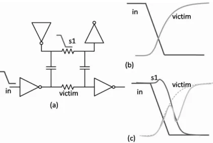
As shown in Figure 2.3(a), the circuit suffers from the crosstalk coupling from the switches of signals. Figure 2.3(b) shows the ideal signal transmission without the crosstalk effect; the curve in the light color represents the victim net from the input signal displayed in the heavy line. However, if the aggressor line s1 switches in the opposite direction of the victim net, the crosstalk will impact on the victim net which is displayed in Figure 2.3(c). Accordingly, the crosstalk effect can be described in considering two coupling nets based on [7]. In order to simplify the crosstalk model, we assume only the coupling capacitance can be controlled in layout design. Other parameters in crosstalk effect, such as the driver strengths on the aggressor nets or other load capacitances, are modeled in a crosstalk coefficient. For each net i, the crosstalk coefficient from net j can be formulated in a real number eij ∈ [1, 0], which
Figure 2.3: The crosstalk effects on a circuit. (a)An example of the coupling effect from the switch of a signal in a combinational circuit. (b)The ideal signal transmis-sion without the coupling effect on the victim net (c)The real signal transmistransmis-sion coupling by a switch from high to low of the signal s1 on the victim net.
is the crosstalk on net i contributed by one unit of coupling capacitance from net
j. Instead of using exhaustive timing analysis, which characterizes all cases of the
crosstalk effects from other nets, we use the summation of all effects from other nets as the total crosstalk on one net illustrated in the following equation:
Xtalki =
X
j6=i
eijCij (2.5)
where Cij is the coupling capacitance between net i and net j. Furthermore, we
assume coupling capacitance only exists between neighboring parallel wires because the coupling capacitance decreases rapidly if an element is far away from the other elements. Also, the coupling capacitance between perpendicular wires is so small that it can be ignored. For these reasons, the coupling capacitance can be stated by the following formula:
C = α length
distanceβ (2.6)
2.3
Problem Formulation
Employing these definitions, we attempt to use a simple but reliable crosstalk model to estimate the coupling capacitance in the technology mapping stage. In order to construct an accurate model, we also employ the companion placement to determine the layout information, such as wire delay and wire load. Consequently, the problem we concern about is described as follows:
Given a subject graph of a network and a library of gates, generate a mapped netlist which could minimize the crosstalk noise effects based on a reliable crosstalk model under specified delay constraints.
Chapter 3
Algorithm for Crosstalk-Aware
Technology Mapping under Delay
Constraints
In this chapter, we first present the overall methodology of our crosstalk-aware technology mapping. Then, the explanation of our technology mapping algorithm is divided into two subsections to illustrate—the matching phase and the covering phase. In the matching phase, we will explain our virtual layout generation for estimating crosstalk. The covering algorithm targeting crosstalk is then described.
3.1
Our Methodology
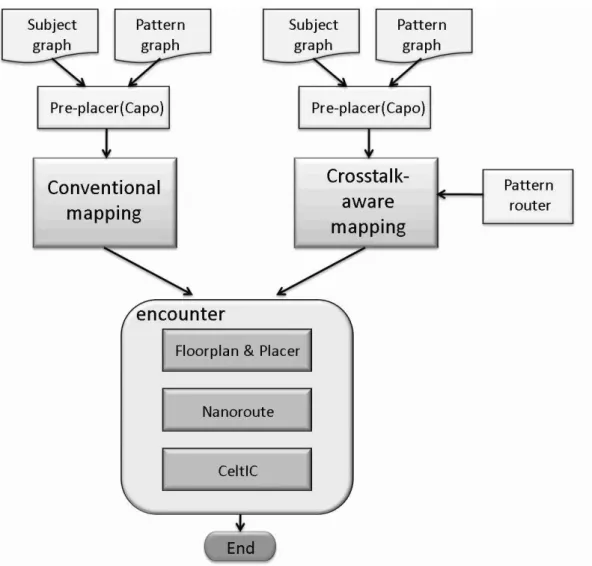
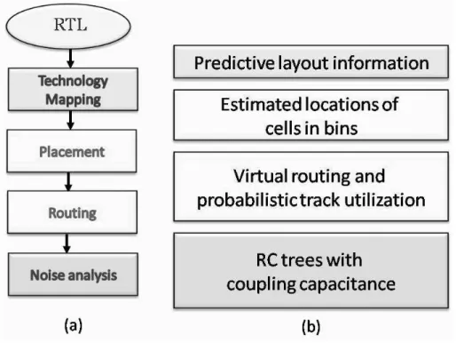
As revealed by Figure 3.1(a), the general design flow from the circuit design in RTL to the physical design ending in noise analysis can be typically described in the five steps. As can be seen, the noise analysis requires RC-trees with coupling capacitance to determine crosstalk effects. For this reason, if crosstalk is considered in the technology mapping, the methodology in predicting layout information would be essential as shown in Figure 3.1(b). Before computing the coupling capacitance, it is necessary to route the wire connections and to predict the track utilization. Therefore, we can not only adopt a companion placement to estimate the locations of each match, like the traditional technology mapping. In addition, a quick global
Figure 3.1: The overview of our methodology in predicting layout information. (a)A desgin flow divided into five stages from the RTL design to the physical noise anal-ysis. (b)The corresponding process for each phase to predict the layout information in technology mapping.
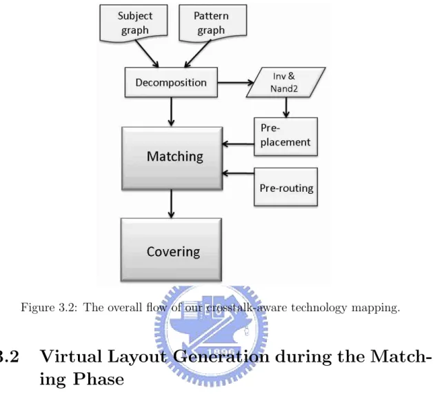
router has to be employed to predict the wire routing in our matching phase. The overall flow of the proposed technology mapping is shown in Figure 3.2. Before the matching phase, in order to consider the wire-loads and wire-delay, a com-panion placement is employed to generate the layout information. In the matching phase, a virtual routing process estimates the net connections of each candidate match to evaluate their contributions to crosstalk. As a result, the whole map can be constructed during the covering phase, and then the optimal crosstalk solution can be chosen from the candidate matches in load-delay curve based on the estima-tion of crosstalk cost which is associated with the probabilistic extracestima-tion method from [21].
Figure 3.2: The overall flow of our crosstalk-aware technology mapping.
3.2
Virtual Layout Generation during the
Match-ing Phase
The matching phase of delay-driven technology mapping exploiting dynamic pro-gramming scheme normally involves storing a load-delay curve at each node of the abstract network. After generating all matches by comparing the pattern graph to the subject graph, only the non-inferior matches, which minimize the delay for different load values, would be collected in the curve. During the construction of the curve, wire-loads and wire-delays are calculated based on the relative locations of each match from the companion placement. To evaluate the contributions to crosstalk of each mapping solution, the determination of each net connection is necessary; hence, we associate a simple pattern routing with the match phase, as presented in the following subsections.
3.2.1
Bottom-up Virtual Routing Map Construction
Figure 3.3: The explanation of pre-placement and pre-routing in the matching phase. (a) An example of a matched gate with its fanins’ and fanouts’ rectangles, the new position of this gate is the gravity center of these rectangles [11]. (b) The corresponding virtual routing map in bins for the gate and its fanins. The rectangles in dotted line are the routing windows for L- or Z- shape routing patterns. Our quick router would choose the appropriate patterns with least congestion.
To create a global as well as a partial view of layout, the new position of each match is calculated in the gravity center of its fanins’ and fanouts’ rectangles, affirmed as a better location than the center of mass of the merged nodes 1 in [11], as revealed in Figure 3.3(a) . After that, the fanin nets of each match are routed and stored in virtual routing map at each match. Due to the reduction in run time of programs, a quick global router is utilized to estimate routing topology. We use an L- and Z-shape pattern routing algorithm [22] skipping the layer assignment phase. It would choose the appropriate path in the sparser region of the routing rectangle, thus reducing congestion and constructing a partial routing map storing in each match, as can be seen in Figure 3.3(b). These partial maps only specify the relevant wires of the transitive fanin cone of a given node, not for the entire network.
1The mass of the merged nodes is the list of network nodes which are covered by a match. The
Hence, they just represent a partial map in the relationship of the connection wires for a given node. Accordingly, a complete map would be generated in the end of the matching phase after visiting each node topologically. For these reasons, we postpone the crosstalk computation in the covering phase.
3.2.2
Handling Multiple Fanouts
For the multiple fanout points, we regard a multi-terminal net as several two-pin nets handling in the input points of its next gates, for the determination of routing nets is from the fanin nets in each match. According to the similar consideration from [14, 23], the crosstalk cost of the virtual map can be divided by the number of fanouts2. In [23], the cost is the summation of the gate-area in each node, which is minimized under delay constraints. In this work, we employ the same concept in our virtual routing map. Thus, the crosstalk cost based on the virtual routing map at primary outputs can be computed by the bin-wise summation of the corresponding routing maps.
3.2.3
Comparison with Recent Works in Technology
Map-ping
According to the analogous approach in [14] which targets routing congestion under delay constraints, our approach considers crosstalk noise under the same constraints. We adopt the identical frameworks, the load-delay curves and a pre-placement, to handle the accuracy of delay. In [14], it uses the congestion map based on the probabilistic method to predict the tendency of routing congestion. However, the measurement of congestion and that of crosstalk are extremely distinct. Crosstalk has to be estimated by the coupling capacitance of each net segment, just as shown
2The original idea in [23] is that the visiting numbers of a node in the preorder traversal during
the covering phase is the same as its fanout numbers. In order to avoid doubling cost in the second time of visiting, the costs have to be divided by the number of traverse.
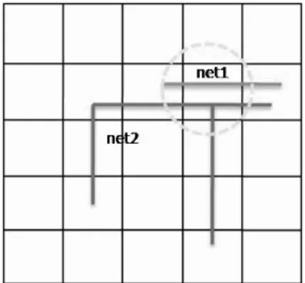
Figure 3.4: The coupling capacitance of a unit segment on net 2 is contributed by net 1, so the routing for net 1 and net 2 has to be determined.
in Figure 3.4, whereas congestion only needs to be assessed from the distribution of net routing. This is the reason why [14] can use probability to represent the net paths, but a routing step is critical here. Only if the net connection is determined, the coupling capacitance can be measured and the relationship between adjacent nets will be meaningful.
3.3
Crosstalk Minimization under Delay Constraints
during the Covering Phase
Figure 3.5: Six configuraions of adjacent nets. The bold net is the net under con-sideration; dotted nets represent empty tracks.
Based on the complete map in wire routing from the matching phase, we can evaluate the crosstalk noise by the probabilistic extraction method [21] in the cov-ering phase. The probabilistic extraction method employs the probability of track utilization to estimate the unit length coupling capacitance for a net segment. It
enumerates the possible density configurations of the net with respect to all the other nets sharing the same segment. In addition, the probabilities from these dif-ferent configurations would be regarded as the weight for averages of per unit length capacitance values. In [21], it defines six possible configurations which would cause valid coupling capacitances between the adjacent nets shown in Figure 3.5. There-fore, the unit coupling capacitance weighted by the probability of each configuration can be stated in the following:
coupling captotal(i) = coupling cap(i)×
conf(i)
total conf igurations (3.1)
where coupling cap(i) is a pre-computed per unit length coupling capacitance of the
i-th configuration, and the total-configurations can be described as total conf igurations =
n
k
k! (3.2)
where n is the number of tracks and k is the track utilization. Finally, the coupling capacitance of each net can be calculated by summing the weighted contributions for all configurations and scaling with the length of the net segment shown in
coupling cap(k) = length(k) · X
i∈conf
coupling captotal(i) (3.3)
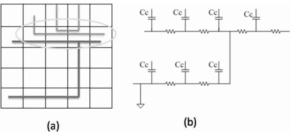
As a result, we can translate the virtual routing map to a crosstalk map com-posed of coupling capacitances and wire resistances, as shown in Figure 3.6. The crosstalk map is also separately described in vertical parts and horizontal parts, just the same as the virtual routing map.
To improve the crosstalk of the solutions and still preserve the timing con-straints, we do not choose the delay-optimal one at each node like the traditional delay-oriented technology mapping. Instead, the solution with less crosstalk and positive slack, which is defined the difference between the required time and the arrival time, would be selected to replace the delay-optimal one with more crosstalk
Figure 3.6: An example of a routing map and its corresponding RC tree. (a) An example of the routing map and the thicker net is under consideration. (b) The corresponding coupling capacitance and wire resistances tree for the thicker net in horizontal direction.
in the load-delay curves. Besides, the cost function is not only considering crosstalk issue but also containing congestion subject. Since the coupling capacitance is com-puted by each net segment of the fanins at each match in the local region, the solution with lower crosstalk might create other solutions which possibly tend to increase congestion globally. For this reason, we still consider congestion which cer-tainly takes account of the global picture at the same time. The congestion factor we adopt in our cost function is from [14] corresponding to the total track over-flow computed by addition of the overover-flow track numbers in the entire map, so we formulate two parameters in the cost function described as follows:
cost = α · crosstalk + β · overf low (3.4)
where α and β are constant coefficients for users adjusting. The crosstalk cost is based on EQ(3.3) to estimate the coupling capacitance values, and the overflow definition is in terms of EQ(2.4) in Chapter 2. Furthermore, in order to access the non-inferior matches in the load-delay curve in comparing with the delay-optimal one, the two parameters in the cost function are defined in the ratio of the non-inferior match to the delay-optimal one of a given node. Based on this cost function,
the following subsection illustrates our covering algorithm.
3.3.1
Algorithm for the Crosstalk-Aware Covering
The pseudo-code for the crosstalk-aware covering procedure under delay constraints is revealed in Algorithm 1. At first, it requires to derive the delay-optimal matches (mD−opt
n ) from the given loads and to calculate the slacks from the delay constraints
at the primary outputs(P O). Then, the entire virtual routing map(RMap) for the delay-optimal solutions is built by the bin-wise addition of the partial maps corresponding to the transitive fanin cone of each match at primary outputs. This map is applied to measure the contributions of all the wires which may appear in the mapped network. It represents the wire distribution based on the conventional delay-optimal solutions. When the complete routing map is constructed, the total overflow (OF ) used to be a comparing base to indicate the routing congestion is estimated by EQ(2.4) for these solutions.
After this initialization, all the nodes in the subject graph are processed in the reverse topological order. First of all, the crosstalk value (Xtalk) and the total track overflow (OF ) would be computed from the delay-optimal match for the given load. Then, these two parameters, the denominators of the cost function, are passed to the procedure that is obtaining the crosstalk-optimal match from the set of the non-inferior matches(Mn), as explained in the next subsection. If the returned cost
of the crosstalk-optimal match (mXtalk−opt
n ) is smaller than one, which means the
estimated crosstalk noise of this match is less than the delay-optimal match, the crosstalk-optimal match will be chosen; otherwise, the delay-optimal one will be stored. In the former case, the routing map should be updated to conform with the modification of this match in its transitive fanin cone; also, the total track overflow and the slack should be updated at the same time. In contrast, if the delay-optimal match is the best choice based the comparison, the slack is simply propagated to
Algorithm 1 The covering algorithm targeting crosstalk minimization under delay constraints
Input: N= subject graph, PO= set of primary output, Mn: sets of non-inferior
matches for Node n∈N, RMapmn= a routing map for Match m at Node n
Output: The mapped netlist for crosstalk-optimal under delay constrants 1. for ∀o∈ P O do
2. choose delay optimal match mD−opt o
3. compute slack So
4. end for
5. RM ap ←P|o|RMapmD−opt o
6. OF ← total track overflow(RM ap)
7. for ∀n∈ N, in reverse topological order do 8. compute XtalkD + OFD for mD−opt
n
9. {costXtalk−opt, mXtalk−opt
n } ← crosstalk optimal match(Mn, Sn, XtalkD, OFD)1
10. if costXtalk−opt< 1 then
11. choose mXtalk−opt n
12. RMap ← RMap − RMapmD−opt
n + RM apmXtalk−optn
13. OF ← OFXtalk−opt
14. compute slack for mXtalk−opt n
15. else
16. choose mD−opt n
17. compute slack for mD−opt n
18. end if
19. increase input loads 20. end for
1 The procedure “crosstalk optimal match(M
n, Sn, XtalkD, OFD)” will be illustrated in Algorithm 2.
the fanins of the match. Finally, it is required to increase the input loads of this match to the predecessors in the subject graph.
3.3.2
Procedure for Obtaining Crosstalk-Optimal Match
un-der Slack constraints
Algorithm 2 explains that how to obtain crosstalk-optimal match (mxtalk−opt
n )
satis-fying slack constraints from the set of non-inferior matches except the delay-optimal one at a given node. Here, the cost function requires the crosstalk value (XtalkD)
and the total track overflow (OFD) of the delay-optimal match as the denominators.
It is clear that if the match satisfies the slack constraints at line 6, the modifica-tion of the routing map (RMap) and the computamodifica-tion of the crosstalk cost will be processed. After that, the comparison will select the match with the smallest cost as the crosstalk-optimal one to return. In fact, the cost function is easily extended to other values for different objectives as demand. In this thesis, we attempt to consider the coupling capacitance and the total track overflow at the same time by the two coefficientsα and β. We adjust them for different benchmark circuits due to different design characteristics.
Algorithm 2 This procedure obtaining the crosstalk optimal match which satisfies the slack constraints
Input: XtalkD= the crosstalk vaule for mD−opt
n , OFD= the overflow for mD−optn
Output: return {costXtalk−opt, mXtalk−opt n }
1. Procedure crosstalk optimal match(Mn, Sn, XtalkD, OFD) {
2. cost ← ∞ 3. if Sn> 0 then
4. for all mn∈ Mn except mD−optn do
5. compute Delay Dmn for mn
6. if Dmn − DmD−optn < Sn then
7. RMap ← RMap − RMapmD−opt
n + RM apmn
8. compute Xtalk + OF for mn
9. costmn ← α ·
Xtalk
XtalkD + β ·OFOFD
10. if costmn < cost then
11. cost ← costmn 12. mXtalk−opt n ← mn 13. end if 14. end if 15. end for 16. end if 17. }
3.3.3
Time Complexity of Our Approach
The time complexity of our technology mapping is almost equivalent to that of a traditional technology mapping. Our matching procedure is similar to a conventional matching one, except that we have to establish and store the virtual routing map, which is associated to the non-inferior matches. Therefore, the computation of the virtual routing map requires O(Nmatches × |Netsmatch|) time, where Nmatches is
the number of non-inferior matches over the entire network and |Netsmatch| is the
number of nets connected with a match, the same as the fanin number of a match. From our employed library, the largest of the fanin number is 6, so |Netsmatch|
can be regard as a constant number. As a result, the matching phase for our approach requires O(Nmatches)time for a given library. During the covering phase, the
function for obtaining the crosstalk optimal match called for all the nodes requires
O(Nmatches×Nbins), where Nbins is the number of bins over the entire layout. In fact,
Nbinsis a constant for a given layout although it might be possibly large as compared
to other constants subsumed by the big-O function. Consequently, we state that our covering algorithm requires O(Nmatches) time, the same as the time complexity
Chapter 4
Experimental Results
4.1
Experimental Setup
Our crosstalk-aware technology mapping was implemented in C programming lan-guage and incorporated in SIS [17], which is a logic synthesis system from UC-Berkeley. The benchmark set we performed was the entire set of ISCAS’85 bench-mark, and the library we utilized in the technology mapping was lib2.genlib in SIS modified with UMC 90 nm technology models. All the benchmarks were tested on a workstation with Dual Core AMD Opteron(tm) Processor 270 and 4 GB mem-ory. The experimental flow was shown as Figure 4.1. When a given benchmark was decomposed into the primitive gates, the subject graph would be placed to generate the pre-placement. Here, we employed Capo [24], a recursive bisectioning-based placer which is publicly available, as our pre-placer. Furthermore, in order to compare fairly, the conventional delay-oriented technology mapping in SIS was modified to contain this pre-placement procedure to estimate the wire-loads and wire-delay. Similarly, our technology mapping not only used the same method to estimate the delay information but also generated the routing information based on this pre-placement. For the delay constraints in a given benchmark, we run the con-ventional technology mapping and widened the critical arrival time at the primary output to 150% as the require time for other primary outputs. After the technology
Figure 4.1: Our experimental flow for the conventional and crosstalk-aware mapping.
mapping, the mapped netlist composed by standard cells would be placed into the SoC Encounter [15], the commercial tool of Cadence, to create the physical layout and noise analysis. In the SoC Encounter, we utilized the technology files from UMC 90 nm library sand set the core utilization of die as 0.8. The post timing and noise analysis were also based on CeltIC, the crosstalk analyzer for cell-based design in SoC Encounter.
4.2
Experimental Results
The experimental results in the comparison of the conventional technology mapping and our crosstalk-aware one based on the post-routing analysis in SoC Encounter are displayed in the Table 4.1 and Table 4.2. Table 4.1 shows the area, number of cells and delay for the benchmarks in Column 1. We could clearly see the increase of area and delay between the conventional mapping and our mapping in percentage in Column 4 and 9. Likewise, in Table 4.2, the improvement of crosstalk and run-time are revealed respectively. We also display the number of the total net and the crosstalk net to explain the crosstalk effects on a circuit. Since the compositions of standard cells in each benchmark created by the conventional mapping and our mapping are varied, we utilize the ratio of the crosstalk net to the total net to express the circuit impacted on the crosstalk noise. In this thesis, the crosstalk noise is represented by the receiver peak, which means the response of the cell to the input glitch applied by coupling effects from other aggressive cells. When a net is recognized as a noise failure, it indicates that the receiver peak value is greater than the receiver threshold we define. Column 4 and 5 of Table 4.2 shows the number of the net with invalid receiver peak. Furthermore, the crosstalk ratio in a whole circuit is shown in Column 6 and 7, and the crosstalk improvement due to our crosstalk-aware technology mapping could be clarified in Column 8. Finally, the run-time is shown in Column 9 and 10. The observation from these tables is explained in the following.
As can be seen in the area columns of Table 4.1, the area on average is increased about 11% as the penalty for the crosstalk reduction. Since the core utilization is set to 0.8, the area of the circuit is directly proportioned to the number of cells. The number of cells in our mapping is also larger than the conventional one. The reason is possible that the delay-oriented mapping would choose larger range of the merged
Table 4.1: The comparison of area and delay between the conventional delay-oriented mapping and our crosstalk-aware mapping. The increase in area and delay shown in percentage is the tradeoff of the improvement in crosstalk for our crosstalk-aware mapping.
Area(um2) Number of cells Delay(ps)
SIS Ours Increase (%) SIS Ours SIS Ours Increase (%)
C432 616.56 717.95 16.4% 178 212 1126 1159 2.9% C499 1418.26 1568.32 10.5% 371 430 856 934 9.1% C880 1145.78 1331.82 16.2% 295 366 1162 1286 10.6% C1355 1447.362 1536.57 6.1% 381 420 888 958 7.8% C1908 1380.33 1651.10 19.6% 371 475 1271 1449 14.0% C2670 1924.59 1967.85 2.2% 472 493 863 903 4.6% C3540 3545.70 4174.23 17.7% 911 1154 1610 1797 11.6% C5315 4211.55 4161.46 -1.2% 1003 985 1055 1162 10.1% C6288 8353.50 9404.11 12.5% 2161 2590 4653 4689 0.7% C7552 6389.44 7289.81 14.1% 1668 2023 1965 1670 -15.0% average 3043.31 3380.32 11.1% 781.1 914.8 1544.9 1600.7 3.6%
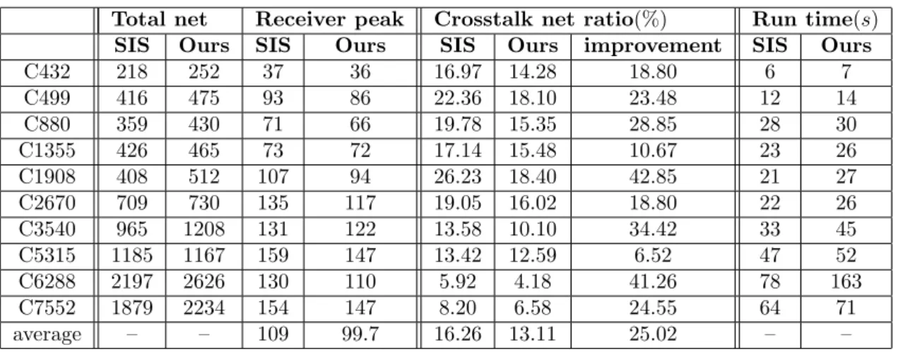
Table 4.2: The comparison of crosstalk noise and run-time between the conventional delay-oriented mapping and our crosstalk-aware mapping. The crosstalk ratio of number of the receiver peak net to number of the total net is shown in percentage. The crosstalk noise for our crosstalk-aware mapping exactly improves up to 25% by experiments.
Total net Receiver peak Crosstalk net ratio(%) Run time(s)
SIS Ours SIS Ours SIS Ours improvement SIS Ours
C432 218 252 37 36 16.97 14.28 18.80 6 7 C499 416 475 93 86 22.36 18.10 23.48 12 14 C880 359 430 71 66 19.78 15.35 28.85 28 30 C1355 426 465 73 72 17.14 15.48 10.67 23 26 C1908 408 512 107 94 26.23 18.40 42.85 21 27 C2670 709 730 135 117 19.05 16.02 18.80 22 26 C3540 965 1208 131 122 13.58 10.10 34.42 33 45 C5315 1185 1167 159 147 13.42 12.59 6.52 47 52 C6288 2197 2626 130 110 5.92 4.18 41.26 78 163 C7552 1879 2234 154 147 8.20 6.58 24.55 64 71 average – – 109 99.7 16.26 13.11 25.02 – –
nodes in the network due to their less delay summing in the whole path. However, our crosstalk-aware mapping does not consider the least delay of the matches on each node, whereas the delay of a match with least crosstalk cost satisfying the slack constraints would be selected; which might cause smaller range of the merged nodes to be chosen. The only exception of the benchmarks is the case of C5315. It might result from the circuit characteristic of this benchmark, which is shorter delay path relative to larger size of circuit comparing with other benchmarks in the entire benchmark set.
From the delay columns in Table 4.1, our crosstalk-aware mapping would create the incremental delay slightly comparing with the conventional mapping, which maintains the delay-optimality. The largest increase of delay is in the case of C1908, while the smallest one is in the case of C6288. In the setting of the delay constraints, the extension of the maximum arrival time from the conventional mapping solutions would cause such increment in the delay of our mapping solutions. However, it is under our consideration. The different result of delay is based on the circuit structure of each benchmark, and it may probably cause decrement in delay, just the same as the case of C7552. In addition, the calculation in the technology mapping is not as precise as the timing analysis in the post-routing, so the inaccuracy can not be avoid.
Our crosstalk-aware technology mapping has been consistently able to reduce the number of net with valid receiver peak value, as shown in Column 8 of Table 4.2. The improvement of crosstalk is exactly 25% on average. Although we use the representation in ratio form to display the improvement of crosstalk, the real number of net with noise failure is authentically reduced as shown in Column 4 and 5. This improvement is promising, especially since the mapped netlists are re-placed without utilizing the pre-placement information from the technology mapping. In fact, we also attempt to insert the companion placement information to the real placement,
but this pre-placement information is just the estimation in the synthesis process. It is not real placement under the physical consideration and may cause larger area or worse delay in reality. Nerveless, in our experiment to pass the pre-placement information at physical placement stage, the crosstalk noise is still reduced in our mapping comparing with the conventional mapping.
Finally, the run-time during the technology mapping is as reveled by Column 9 and 10. On an average, our run-time is nearly 1.4 times worse, but still practical. It demonstrates that the constants in the time complexity O(Nmatches) we analyze
in Section 3.3.3 are not too dominating. In Figure 4.2, to display the result visibly, we show the comparison of crosstalk improvement in histogram normalizing the conventional mapping.
Figure 4.2: The crosstalk improvement results comparing between the conventional delay-oriented mapping (SIS) and Our crosstalk-aware mapping (SIS Xtalk). All the data of ours are normalizing to SIS.
Chapter 5
Conclusions
In this thesis, we have presented a technology mapping algorithm targeting crosstalk noise. We have proposed a procedure in which the coupling capacitance can be es-timated by the predictive layout information based on a reliable crosstalk model. In our matching phase, we have shown how to construct the virtual routing map by a quick pattern router for determining the connection of fanin nets in the non-inferior matches. Our covering procedure, which estimates the coupling capaci-tance by the probabilistic track utilization based on the virtual routing, employs the crosstalk cost function involving two parameters—the coupling capacitance and the total track overflow to consider congestion and crosstalk at the same time. Fi-nally, the mapped netlists are generated by selecting the crosstalk-optimal matches satisfying the slack constraints instead of the delay-optimal ones. The experimental results on ISCAS’85 benchmarks prove that the algorithm is effective. They show that the crosstalk is highly enhanced to 25% on the average as compared to the conventional mapping. We believe that these results might be further improved by the crosstalk consideration in both synthesis stage and physical design stage. The estimated crosstalk information can be propagated to the physical placement and routing, or even the mapped solution can be modified by the feedback information from the physical stage. This orientation can be focused as our future work.
Bibliography
[1] H. B. Bakoglu. “Circuits, Interconnections and Packaging for VLSI”. Addison-Wesley Publishing Company, 1990.
[2] T. Xiao and M. Marek-Sadowska. “Crosstalk Reduction by Transistor Siz-ing”. In Proceedings IEEE/ACM Design Automation Conference, pages 137– 140, Jan. 1999.
[3] M. R. Becer, D. Blaauw, I. Algor, R. Panda, C. Oh, V. Zolotov, and I. N. Hajj. “Post-Route Gate Sizing for Crosstalk Noise Reduction”. In Proceedings of the
International Symposium on Quality Electronic Design, pages 171–176, Mar.
2003.
[4] M. Hashimoto, M. Takahashi, and H. Onodera. “Crosstalk Noise Optimization by Post-Layout Transistor Sizing”. In Proceedings International Symposium on
Physical Design, pages 126–130, Apr. 2002.
[5] I. H.-R. Jiang, S.-R. Pan, J.-Y. Jou, and Y.-W. Chang. “Optimal Reliable Crosstalk Driven Interconnect Optimization”. In Proceedings IEEE/ACM
In-ternational Conference on Computer-Aided Design, pages 128–133, Apr. 2000.
[6] D. Sinha, H. Zhou, and C. C.-N. Chu. “Optimal Gate Sizing for Coupling-Noise Reduction”. In Proceedings International Symposium on Physical Design, pages 179–181, Apr. 2004.
[7] H. Zhou and D. F. Wong. “Global Routing with Crosstalk Constraints”. In
Proceedings IEEE/ACM Design Automation Conference, pages 374–377, Jun.
1998.
[8] H. Zhou and D. F. Wong. “Crosstalk-Constrained Maze Routing Based on Lagrangian Relaxation”. In Proceedings IEEE International Conference on
Computer Design, pages 628–633, Oct. 1997.
[9] J. Lou and W. Chen. “Crosstalk-Aware Placement ”. In IEEE Design and Test
of Computers, pages 24–32, Jan. 2004.
[10] H. Ren, D.-Z. Pan, and P. G. Villarubia. “ True Crosstalk Aware Incremental Placement with Noise Map”. In Proceedings IEEE/ACM International
Confer-ence on Computer-Aided Design, pages 402–409, Nov. 2004.
[11] M. Pedram and N. Bhat. “Layout Driven Technology Mapping”. In Proceedings
IEEE/ACM Design Automation Conference, pages 99–105, Jun. 1991.
[12] Q. Liu and M. Marek-Sadowska. “Wire Length Prediction-Based Technology Mapping and Fanout Optimization ”. In Proceedings International Symposium
on Physical Design, pages 145–151, Apr. 2005.
[13] R. S. Shelar, S. S. Sapanekar, P. Saxena, and X. Wang. “A Predictive Dis-tributed Congestion Metric with Application to Technology Mapping”. In IEEE
Transactions on Computer-Aided Design of Integrated Circuits and Systems,
volume 24, pages 696–710, May 2005.
[14] R. S. Shelar, P. Saxena, X. Wang, and S. S. Sapatnekar. “An Efficient Tech-nology Mapping Algorithm Targeting Routing Congestion under Delay Con-straints”. In Proceedings International Symposium on Physical Design, pages 137–144, Apr. 2005.
[15] “Encounter Text Command Reference”. Cadence Desgin Systems, 2007. [16] G. D. Micheli. “Technology Mapping of Digital Circuits ”. In Proceedings
of Annual European Computer Conference on Advanced Computer Technology, Reliable Systems and Applications., pages 580–586, May 1991.
[17] E. M. Sentovich et al. “SIS: A System for Sequential Circuit Synthesis”. In
Memorandum No. UCB/ERL M92/41, May 1992.
[18] D. Pandini, L. T. Pileggi, and A. J. Strojwas. “Global and Local Congestion Optimization in Technology Mapping”. In IEEE Transactions on
Computer-Aided Design of Integrated Circuits and Systems, pages 498–505, Apr. 2003.
[19] J. Rabaey. “Digital Integrated Circuits: A Design Perspective”. Prentice-Hall, 1996.
[20] T. Sakurai and K. Tamaru. “Simple Formulas for Two and Three Dimensional Capacitance”. In IEEE Transactions on Electron Devices, Feb. 1993.
[21] M. Becer, D. Blaauw, R. Panda, and I. Hajj. “Pre-Route Noise Estimation in Deep Submicron Integrated Circuits”. In Proceedings of the International
Symposium on Quality Electronic Design, pages 413–418, Mar. 2002.
[22] H.-M. Chen, H. Zhou, F.-Y. Young, D. F. Wong, H.-H. Yang, and N. Sher-wani. “Integrated Floorplanning and Interconnect Planning ”. In Proceedings
IEEE/ACM International Conference on Computer-Aided Design, pages 356–
359, Nov. 1999.
[23] K. Chaudhary and M. Pedram. “A Near Optimal Algorithm for Technology Mapping Minimizing Area uder Delay Constraints”. In Proceedings IEEE/ACM
[24] J. A. Roy and I. L. Markov. “Seeing the Forest and the Trees: Steiner Wire-length Optimization in Placement ”. In IEEE Transactions on Computer-Aided
Design of Integrated Circuits and Systems, volume 26, pages 632–644, Apr.
作者簡歷
范芳瑜,民國七十二年九月出生於新竹縣,於新竹定居。民國九十五年六月畢業 於國立交通大學電子工程係,並於同年九月進入國立交通大學電子研究所系統組, 民國九十七年八月碩士畢業。
![Figure 3.3: The explanation of pre-placement and pre-routing in the matching phase. (a) An example of a matched gate with its fanins’ and fanouts’ rectangles, the new position of this gate is the gravity center of these rectangles [11]](https://thumb-ap.123doks.com/thumbv2/9libinfo/8134222.166367/24.892.149.747.216.506/figure-explanation-placement-routing-matching-rectangles-position-rectangles.webp)