國立交通大學
光電工程研究所
碩士論文
以聚乙二醇為添加物製作高效能負型有機薄膜電晶體
High-Performance n-channel organic thin-film
transistors incorporating poly(ethylene glycol)
研究生:蔡宗翰
指導教授:陳方中 博士
以聚乙二醇為添加物製作高效能負型有機薄膜電晶體
High-Performance n-channel organic thin-film
transistors incorporating poly(ethylene glycol)
研 究 生:蔡宗翰
Student:Tzung-Han Tsai
指導教授:陳方中 博士
Advisor:Dr. Fang-Chung Chen
國 立 交 通 大 學
光電工程研究所
碩 士 論 文
A Thesis
Submitted to Institute of Electro-Optical Engineering College of Electrical and Computer Engineering
National Chiao Tung University In Partial Fulfillment of the Requirements
For the Degree of Master In
Electro-Optical Engineering July 2010
Hsinchu, Taiwan, Republic of China
以聚乙二醇為添加物製作高效能負型有機薄膜電晶體
學生︰蔡宗翰 指導教授︰陳方中
國立交通大學光電工程研究所
中文摘要
本研究選用聚乙二醇,將其添加至負型[6,6]-phenyl C61-butyric acid methyl ester (PCBM) 有機薄膜電晶體之主動層中,研究其對元件特性之影響。由實驗結果可知添加 適當比例之高分子量聚乙二醇能夠有效的提高元件效能並且表現出較好的穩定性。在本 研究中,加入聚乙二醇之元件載子遷移率可由 0.014 cm2 /Vs 提升至 0.044 cm2/Vs,而臨 界電壓也可由 17V 縮小至-2V。在大氣環境下量測,未添加聚乙二醇之元件載子遷移率 變為原本之千分之一,而添加聚乙二醇後則為十分之一。這可歸功於聚乙二醇分子與鋁 電極產生化學反應,進而減少電子注入障礙。
ii
High-Performance n-channel organic thin-film
transistors incorporating poly(ethylene glycol)
Student: Tzung-Han Tsai Advisor: Dr. Fang-Chung Chen
Institute of Electro-Optical Engineering
National Chiao Tung University
Abstract
This study investigates the effect of blending of poly(ethylene glycol) (PEG) into the active layer on the performance of n-channel organic thin-film transistors (OTFTs) based on [6,6]-phenyl C61-butyric acid methyl ester (PCBM). We found that the performance and the stability of the OTFTs could be enhanced after the addition of PEG. The mobility could be improved from 0.014 to 0.044 cm2/Vs, and the threshold voltage shifted from 17V toward to -2V. In the ambient conditions, the mobility of the pristine-PCBM device degraded by three orders. However, the one of the device prepared with PEG only decreased by one order. The enhancement could be attributed into the reduction of the electron injection barrier due to the chemical reactions between PEG molecules and Al atoms of the source/drain electrodes.
謝誌
這個世代的人在中學時期一定會上過這樣一堂國文課,那就是陳之藩的《謝天》, 文中提到:「要謝的人太多了,就謝天吧。」但我想這也許是我一生中唯一一次有機會 可以好好的謝謝大家,所以還是一一說起吧。 能走到今天這一步,最應該要感謝的,就是我的家人,從小到大,爸媽為了哉培我 跟弟弟,省吃儉用,寧願自己用最差的,也要讓我們用最好的,小的時候,爸爸一年三 百六十五天幾乎天天在工作,只為了讓我們有更好的生活,媽媽身體不好卻還是不顧健 康的去擺攤,但當時年紀還小的我卻無力改變什麼,高中時貪玩荒廢課業,讓你們失望。 現在不一樣了,你們的努力總算沒有白費,未來你們好好休息,這個家,換我來付出。 來實驗室的兩年,衷心感謝陳方中老師的指導,老師總是不保留的將自己所學以及 經驗與大家分享,不管是在研究上或是處事方法,都使我有更深一層的見解,也因此在 思考一件事情時我也開始變的有條理,如何從零開始的完成一件事更是讓我終身受用。 再來要感謝博士班的學長 KOBE、志力、孝信、兆峰,我常會會問一些對你們來說很 簡單的問題,但你們卻願意耐心地替我解答,讓我能順利的完成研究。畢業的學長姐們, 阿寬、曾博、+0、POPO、達爾、小公主,謝謝你們在我碩一時的協助,一開始對這個領 域完全沒概念的我,已經有了成長,和你們相處很愉快,碩士生活也因此有了更多樂趣。 最要感謝的就是同屆一起打拚的這一群人了,首先要感謝的就是浩智,感謝你總是 願意放下自己手邊的事來幫我處理一些雜事,實驗上因為你聰明的頭腦,幫我解決了很 多問題,且你總是願意配合我來娛樂大家,祝你一切順利。再來要感謝阿凱、阿達、洪 毅,說起來我們是真正同屆的伙伴,從開始的不熟識直到現在已經要各奔東西,兩年來 不管是在實驗或是生活上的互相協助都讓我感受到出外靠朋友的溫馨,未來有機會要多 相聚。再來要感謝 500,不愧是有機電晶體一哥,跟你討論總能在你身上學到東西,重 點是感謝你還帶我去打壘球,讓我在這兩年還能體會到在紅土場上奔馳的快感,希望還 有機會一起打球。還有老薛感謝妳常關心我以及拿東西給我吃,未來也要一起加油。還 有學弟紹棠、小白,你們適時的協助總是很重要,謝謝你們,你們也要順利畢業。 感謝這兩年來一起來到新竹一起努力的林 JJ 跟噗弟,在我難過低潮時總是與我一 同分擔,我們總是分享彼此的好與壞,在中興的四年裡,一起玩,一起搞系學會,一起 辦宿營,我們一起完成多少可以讓我們回味無窮的活動,也許未來這樣的機會已經很難 得,希望認識六年的交情跟默契可以一直持續下去。感謝中興物理皇家系壘的所有人, 也許我們總是差一個冠軍,但那些努力的過程絕對是最真實的。還要感謝鳥鳥、阿昌、 石帥、益安、子欣、阿璇、郭品超、浩呆、阿竹、髒王彥、小尻、綠豆、小飛象、豆子、 小劉…族繁不及備載,這六年來認識你們真好,能順利走到這裡,你們居功厥偉。還要 感謝 SE,從國一一直到大四,從好友到情人,妳總是陪在我身旁,我們的過去將會是我 一輩子最寶貴的回憶。可能還有很多沒提到的人,也謝謝你們。 最後感謝的人是 iihang,謝謝妳讓我找回積極,讓我知道我還能做什麼,這一年中 妳的關心讓我渡過好多低潮,我們的未來還很長,一起走下去吧。iv
Contents
中文摘要 ... i Abstract ... ii 謝誌...iii Contents... iv List of Figures ... viList of Tables ... viii
Chapter 1... 1
Introduction ... 1
1.1 Preface... 1
1.2 Organic Thin-Film Transistors ... 3
1.2.1 Introduction to Organic Semiconductors... 3
1.2.2 Overview of Organic Thin-Film Transistors ... 3
1.2.3 Overview of n-channel Organic Thin-Film Transistors... 4
1.2.4 Introduction to the N-channel Material PCBM ... 6
1.3 Motivation... 7
1.4 Thesis Organization... 9
Chapter 2... 10
Mechanism and Operation ... 10
2.1 Structures of Organic Thin Film Transistors... 10
2.2 The Charge Carrier Transportation in Organic Semiconductors ... 11
2.2.1 Preface ... 11
2.2.2 Polaron and Bipolaron ... 12
2.2.3 Hopping Model... 13
2.2.4 Multiple Trapping and Release Model (MTR)... 14
2.3 The Operation of Organic Thin-Film Transistors ... 14
2.3.1 Energy Level Principle and Carrier Distribution ... 14
2.3.2 The Methods of Extracting Parameters ... 18
Chapter 3... 21
Experimental and Analysis Methods... 21
3.1 Substrate Preparation... 21
3.1.1 Preface ... 21
3.1.2 ITO Patterning Process... 21
3.1.3 Cleaning of ITO/Glass Substrate... 23
3.1.4 Cleaning of SiO2/Si Substrate ... 23
3.2 The Materials ... 24
3.3 Device Fabrication Process of OTFTs ... 25
3.3.1 Spin-Coating Polymer Dielectric Film... 25
3.3.2 Spin-Coating of PCBM/PEG Blends as the Active Layer and Evaporation of Metal Electrodes ... 25
3.4 Measurements and Analysis of OTFTs ... 28
3.4.1 Electrical Characteristics... 28
3.4.2 Capacitance Analysis... 28
3.4.3 Surface Morphology Measurement ... 28
3.4.4 X-ray Photoelectron Spectroscopy Measurement ... 30
Chapter 4... 32
Results and Discussion ... 32
4.1 Characteristics of Device Electrical Properties ... 32
4.1.1 The Effect of Molecular Weight of PEG... 32
4.1.2 The Effect of PEG Concentration... 35
4.1.3 The Electrical Characteristics Measured in the Atmosphere ... 38
4.1.4 The Effect of PEG on the Devices Fabricated on PVP/SiO2 Substrate ... 40
4.2 Morphological Analysis of the Active Films... 43
4.3 Analysis of Device Resistances ... 45
4.4 The Analysis of XPS Measurements... 48
Chapter 5... 49
Conclusion and Future Work ... 49
5.1 Conclusion... 49
5.2 Future Work... 49
vi
List of Figures
Figure 1.1 The application of organic electronics: a “rollable” OFET-driven OLED Display
that can wrap around a pencil... 2
Figure 1.2 The application of organic electronics: a transparent OLED Display. ... 2
Figure 1.3 N-type organic semiconducting materials. ... 5
Figure 1.4 The chemical structure of [6,6]-phenyl C61-butyric acid methyl ester (PCBM)... 6
Figure 1.5 Out-of-plane XRD pattern of spin-coated PCBM film. ... 7
Figure 2.1 Two TFT structures (a) Top contact (b) Bottom contact. ... 10
Figure 2.2 The structure of polarons. ... 12
Figure 2.3 The origin of polaron in energy band ... 13
Figure 2.4 Intermolecular charge carrier hopping... 13
Figure 2.5 (a) The energy level diagram of an OTFT at VG = 0 and VD = 0. (b-e) the mechanism of OTFT operation for the case of electron (b) accumulation and (d) transport; hole (c) accumulation and (e) transport. ... 15
Figure 2.6 (a) Carrier concentration diagram of TFT in the linear regime. (b) Pinch-off occurs when VD ~ VG – VT. (c) Carrier concentration diagram of TFT in the saturation regime ... 17
Figure 2.7 (a) ID –VD curves for a n-OTFT for various VG. (b)ID – VG curves for various VD, and the ID0.5 – VG curve is shown on the right-handed axis... 19
Figure 2.8 The illustration of transfer line method. ... 20
Figure 3.1 The process of ITO patterning. ... 22
Figure 3.2 The structure of organic materials used in this experiments. ... 24
Figure 3. 3 The energy level diagram of the materials used in this study. ... 24
Figure 3.4 The flow chart of the device fabrication process ( ITO/glass substrates). ... 26
Figure 3.5 The flow chart of the device fabrication process ( Si/SiO2 substrates). ... 27
Figure 3.6 The interaction force between two atoms. ... 29
Figure 3. 7 The operation method of AFM. ... 29
Figure 3.8 Basic components of monochromatic XPS system... 31
Figure 4.1 The ID-VD output curves of (a) pure PCBM device, and device prepared with PEG (b) 400, (c) 1000, (d) 3000, (e) 8000, and (f) 20000, respectively. ... 33 Figure 4.2 The (a) ID-VG and (b) ID1/2-VG transfer curves at VD =60V with distinct molecular weight of PEG blending. ... 34 Figure 4.3 The ID-VD output curves of (a) pure PCBM OTFTs, and with (b) 1%, (c) 5%, (d) 8%, (e) 11%, and (f) 16% PEG 20000 blending, respectively... 36 Figure 4.4 The (a) ID-VG and (b) ID1/2-VG transfer curves at VD =60V with distinct concentration of PEG 20000 blending. ... 37 Figure 4.5 The ID-VD output curves of the OTFTs (a) without and (b) with PEG 1500 (5%) blending in the ambient environment... 38 Figure 4.6 The (a) ID-VG and (b) ID1/2-VG transfer curves at VD = 30 V and 60 V of the OTFTs with and without PEG blending in ambient environment. ... 39 Figure 4.7 The ID-VD output curves of the OTFTs prepared (a) without, and (b) with PEG 400 on PVP/SiO2 substrates. ... 40 Figure 4.8 The (a) ID-VG and (b) ID1/2-VG transfer curves at VD = 60 V of the OTFTs with and without PEG blending on PVP/SiO2 substrates... 41 Figure 4.9 The height-mode images measured by AFM :(a)pristine PCBM, (b) to (f) PEG 400 (5%), PEG 1000 (5%), PEG 3000 (5%), PEG 8000 (5%), and PEG 20000 (5%), respectively. ... 44 Figure 4.10 Total resistance as a function of channel resistance at various gate voltages. (a) pristine-PCBM; (b) with PEG 20000 (5%). ... 45 Figure 4.11 The C1s XPS spectra of PCBM/Al with and without PEG... 48
viii
List of Tables
Table 4.1 The parameters of the OTFTs with distinct PEG molecular weight (MW) blending measured in nitrogen filled glove box. ... 34 Table 4.2 The parameters of the OTFTs with different ratio PEG 20000 blending measured in nitrogen filled glove box... 37 Table 4.3 The comparison of transfer characteristics of the OTFTs measured in inert and ambient environment. ... 38 Table 4.4 The parameters of the OTFTs prepared with and without PEG blending on PVP/SiO2 substrates. ... 41 Table 4.5 The continuous measurement parameters of the pristine PCBM OTFT on PVP/SiO2
substrates in N2-filled glove box. ... 42 Table 4.6 The continuous measurement parameters of the PEG (5%) /PCBM OTFT on PVP/SiO2 substrates in N2-filled glove box... 42 Table 4.7 The relationship between hill numbers and mobility with distinct molecular weight (M.W.) of PEG... 43 Table 4.8 Resistance analysis of PEG molecular weight. ... 45 Table 4.9 Resistance analysis of PEG blending ratio. ... 46
Chapter 1
Introduction
1.1 Preface
Over the last few years, the organic electronic devices such as organic light-emitting diodes (OLEDs), organic photovoltaic cells (OPVs), and organic field-effect transistors (OFETs) have received much attention [1, 4]. Because many of the organic or polymer molecules can be dissolved in organic solvents, the solution can be used for large-area fabrication, such as using spin-casting or ink-jet printing processes. Because the production process of organic electronics only requires relatively low temperature, usually less than 200 ℃, plastics could be potentially used as the substrates. However, some problems still remain to be solved. The organic semiconductors are very unstable and sensitive to the environment; the mobility is also much lower than the typical values of inorganic semiconductors.
At Society for Information Display (SID)-2010 electronic-display exhibition in Seattle (May 23-May 28), Sony Corporation announced a flexible, 80 μm-thick, full color OLED display (4.1-inch) driving by OFETs which can be enveloped around a thin cylinder with a radius of 4 mm (Figure 1.1).
In the same conference, Samsung Mobile Display showed their 19-inch transparent AMOLED display. Its transparency is reported to be over 30%. It can deliver the usage in notebook, car windshields, and for storefront advertising. The prototype is shown in Figure 1.2.
2
Figure1.1 The application of organic electronics: a “rollable” OFET-driven OLED Display that can wrap around a pencil. [Adapted from http://en.akihabaranews.com/47902/display]
Figure1.2 The application of organic electronics: a transparent OLED Display. [Adapted from http://en.akihabaranews.com/47796/display]
1.2 Organic Thin-Film Transistors
1.2.1 Introduction to Organic Semiconductors
Organic semiconductors are organic materials within semiconducting properties. We can classify them into two categories: oligomers and polymers. Oligomers consist few repeat units. Oligomers include dimers, trimers and tetramers. OTFTs fabricated from oligomers have been demonstrated with high mobilities (2-40 cm2/Vs) [7, 50].
Polymers are large molecules (macromolecule) which are composed of a long chain made of hydrogen and carbon elements. Bonding occurs when the carbon atoms are brought together. It forms the backbone of the molecule and leaves one weakly π-bonded electron. This π-bonded electron can transport in the polymer while an electric field is applied. Park et
al. demonstrated the TFTs fabricated by the poly(3-hexylthiophene) polymer. They have
relatively lower mobilities (0.04 cm2/Vs) [51].
The most important advantage of organic semiconductors is that they can be processed at lower temperatures, which means they are suitable for flexible plastic substrates. Many developers in this field have high interest in this subject, and try to improve the process techniques.
1.2.2 Overview of Organic Thin-Film Transistors
Organic thin-film transistors (OTFTs) have received much attention from many scientists. The first OTFT was demonstrated in 1983 by F, Ebisawa et al [2]. The authors used polyacetylene and polysiloxane as the active layer and the dielectrics, respectively in the devices. However, the mobility was just 1×10⁻⁵ cm2/Vs and the device did not show pinch-off. In past decade, organic thin-film transistors with improved performance have been reported. In 1997, Lin et al. demonstrated an OTFT, whose mobility was greater than 1 cm2/Vs for the first time [49]. In 2007, Takeda et al. proposed a very high-mobility OTFT which was
4
fabricated with single-crystal rubrene. The maximum mobility is evaluated as high as 40 cm2/Vs [50].
1.2.3 Overview of n-channel Organic Thin-Film Transistors
So far, the electrical performances of p-channel organic OTFTs such like mobility and stability are much better than those n-channel devices. However, the n-channel OTFTs still play important roles in the production of electronics (ex: CMOS inverters). The common n-channel semiconductors are shown in Figure 1.3.
In general, the operation of many n-channel OTFTs is not stable in ambient conditions. It is attributed to its sensitivity to water and oxygen. The organic radical anions are produced in the channel as applying a positive gate voltage. These radical anions have a very high reducing power that can react effectively with water or oxygen. Hence most of n-channel OTFTs can only be measured and operated under inert environment such as in a nitrogen-filled glove box [16-18].
Besides, there are two major challenges that have to be overcome for improving the performance of n-channel OTFTs. First, the electrons are easily trapped by hydroxyl groups at the semiconductor-insulator interfaces. This problem can be solved by using hydroxyl-free polymer insulator materials [17, 31]. For example, a special kind of polyvinyl alcohols (Mowiol® 40-88) has been used as the gate insulator material and formed an electron-trap-free interface [31].
The second issue of enhancing the performance of n-channel OTFTs is their poor injection of electrons from the source/drain (S/D) electrodes into the semiconducting layer. For high-performance n-channel OTFTs, electrons need to inject efficiently into the lowest unoccupied molecular orbitals (LUMOs). The LUMO of the organic semiconductor usually locates at around 2 to 3 eV verse the vacuum energy level. Better electron injection can be
achieved by introducing low work function metals, such as Ca, Al, and Mg. However, all these metals are very unstable under ambient environmental. Cho et al. demonstrated n-channel OTFTs inserting titanium sub-oxide (TiOx) at the electrodes/semiconductor interface [52]. This method can not only effectively improve the electron injection but also protect the channel from the influence of the environmental. Now for n-channel materials, the mobility up to 6 cm2/Vs has been improved using fullerene molecules made through vacuum evaporation as the active material [23, 24].
6
1.2.4 Introduction to the N-channel Material PCBM
Fullerene molecules have a high electron affinity and have been widely used for fabrication of high-performance n-channel OTFTs [23, 24]. In this study, a fullerene derivative, [6,6]-phenyl C61-butyric acid methyl ester (PCBM), has been chosen as the organic semiconductor. PCBM is solution-processable and its chemical structure is shown in Figure 1.4.
Figure1. 4 The chemical structure of [6,6]-phenyl C61-butyric acid methyl ester (PCBM) [22].
The highest occupied molecular orbital (HOMO) of PCBM is about -6.1 eV and the lowest unoccupied molecular orbital (LUMO) of PCBM is about -3.7 eV. Researchers have chosen PCBM as an electron acceptor and a conducting polymer, poly(3-hexylthiophene) (P3HT), as an electron donor to form the most successful model materials system for organic photovoltaic. Power conservation efficiencies of these bulk heterojunction polymer photovoltaic cells have been reported to be around 5%, and these devices also exhibited thermal stability [53].
Nevertheless, less attention has been paid to the morphology of pristine PCBM. In general, the spin-coated PCBM thin film forms disarranged structure [21]. No diffraction peaks and homogeneous morphology were observed in the PCBM thin film from the the results of X-ray diffraction (XRD) and the atomic force microscope (AFM) measurements
[20], which are shown in Figure 1.5.
Figure1.5 Out-of-plane XRD pattern of spin-coated PCBM film. Inset shows AFM image of PCBM film [20].
Recently, PCBM has showed its high performance with high electron mobility up to 0.03 -0.04 cm2/Vs [22, 37]. It points that PCBM can act as a good semiconductor material for n-channel organic devices and as a building block for organic CMOS semiconductor circuits.
1.3 Motivation
In recent years, the highest mobility of n-channel Organic thin-film transistors (OTFTs) reported is up to 6cm2/Vs for fullerene molecules by vacuum deposition [23, 24]. However, to take the advantages of low cost and easy processing, solution-processed OTFTs are needed. Mobility values from 0.18 to 0.9 cm2/Vs are already obtained with high ON/OFF ratios for
the solution-processed p-type materials [25-28], although the n-type solution-processed OTFTs are still lagging in performance.
The solution-processed fullerene derivatives are known as potential candidates for high-performance n-channel OTFTs [18-20, 29-31]. Higher electron mobility with
8
low-work-function calcium S/D electrodes were also reported [32], but these metals are easily oxidized and, therefore, the devices need further passivation.
An alternative approach for replacing the reactive metals as an electrode is to insert a thin layer of alkali metal halides [33] or carboxylates [34], in various efforts for improving the charge injection from an Al cathode to an emitting layer for organic light emitting diodes (OLED). Similarly, the S/D contacts in the OTFTs have significant influence on device operation. For example, it has been reported that the electrical properties of n-channel OTFTs can be enhanced by inseting a nanoscale Cs2CO3 interfacial layer between the PCBM active layer and the S/D electrodes [37]. The presence of the Cs2CO3 layer at the organic/Al interface reduced the contact barriers and provided protection against diffusion and chemical interaction between the organic film and metal electrodes. But all the above-mentioned method needed many fabrication steps.
Vertical segregation between organic molecules and its application toward improving the performance of organic electronic devices have become topics of strong research activity [38-44]. To enhance the efficiency and increase the stability of polymer solar cells, Chen et al. introduced a nanoscale functional interlayer, containing poly(ethylene glycol) (PEG) through spontaneous vertical phase separation [44]. During the spin-coating process, the PEG molecules migrated to the surface and formed a thin layer on top of the active polymer layer without the need for any additional fabrication steps. After thermal deposition, the chemical interaction between the PEG monolayer and the Al atoms lowered the barrier height and contact resistance. As a result, the device performance has been improved.
Although high-performance devices made of solution-processed fullerene derivatives have been reported, most of them need additional fabrication steps to modify or protect the active layer. We try to develop a simple fabrication method that made the active thin-film containing poly(ethylene glycol), intend to achieve the same results in one step.
1.4 Thesis Organization
This thesis is organized as followings. In this chapter, the background of this study is described briefly; and in the following chapter, we have introduced the basic mechanism and device structures of organic field-effect transistors. The useful methods of analysis are also presented in this part. The experimental details are shown in the third chapter and the organization of OTFT is illustrated including substrate preparing and thin-film coating. Except for the device fabrication, the analysis methods are also particularly taken into consideration. In Chapter 4, there are discussions for devices prepared with and without blending poly(ethylene glycol) (PEG). Further, the role of PEG in the semiconducting layer is investigated by using atomic force microscope (AFM) and X-ray photoelectron spectroscopy (XPS). Finally, conclusions and future work are remarked in last chapter.
10
Chapter 2
Mechanism and Operation
2.1 Structures of Organic Thin Film Transistors
The conventional field-effect transistors (FETs) are based on the inorganic materials such as Si and Ge. The common FETs are metal-oxide-semiconductor field-effect transistors (MOSFETs). The MOSFETs are used extensively in digital circuits. Because of its relatively small size, millions of devices can be fabricated in a single integrated circuit (IC). The structures of thin-film transistors (TFTs) are similar to FETs, and the main difference is the thickness of active layer.
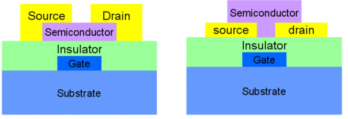
If we replace the inorganic semiconductor with organic semiconductor, the new device is called organic thin-film transistors (OTFTs). According the order of depositing semiconducting materials, OTFTs are classified to two structures: top-contact (TC) and bottom-contact (BC). While the active layer is deposited first, and source and drain (S/D) electrodes are fabricated lately, the structure is called TC. But the BC structure is opposite. The two different OTFTs structures are shown in Figure 2.1.
General speaking, because of the poor adhesion of organic molecules on metal surface, it provides a bad growth base for the active layer. Therefore the device performances of TC OTFTs are better than BC OTFTs due to the small contact resistance at the semiconductor/electrodes interface. But the photolithography process cannot be used after depositing the active layer due to the damage of organic materials during the etching process. Hence we usually use the shadow mask to define the channel length, and the length scale is limited to 40 μm. We have to introduce BC structure to fabricate the smaller length device.
2.2 The Charge Carrier Transportation in Organic
Semiconductors
2.2.1 Preface
The molecular interaction between organic semiconductors is different than inorganic semiconductors. They are covalent bonding and van der Waals force in inorganic and organic molecules, respectively. There are two distributions of -bonding electrons in organic materials: localized states and delocalized states. The definition of localized states is that the electrons are bound to particularly atom. On the contrary, we can find some free electrons in -bonding without direct relationships to specific atom, they are called delocalized states. The carriers in inorganic semiconductor materials are all delocalized states due to the extended bandgap. By the confinement in localized states, the mobility of organic semiconductor is relatively lower than that of inorganic semiconductor.
Up to now, the charge carrier transportation in organic semiconductors is still unobvious. There are three common models in organic semiconductors: polaron and bipolaron [8], hopping [54], and multiple trapping and release models [46].
12
2.2.2 Polaron and Bipolaron
The polaron is an electron or a hole in a conjugated molecule systems together with a cloud of phonons that is result from the deformation of the lattice produced by the interaction of the charges. The energy level is rearranged and the new one is defined as polaron energy level. The polaron structure is shown in Figure 2.2.
Figure 2.2 The structure of polarons. [Adapted from http://upload.wikimedia.org/ wikipedia/commons/d/d0/Polaron]
When two polarons are close together, they can lower their energy by sharing the same deformations, which leads to an effective attraction between the polarons. If the interaction is sufficiently large, then the attraction leads to a bound bipolaron, thereby forming bipolaron energy levels. The origin of polaron in the energy band is shown in Figure 2.3.
If there are many bipolarons in conjugated molecules, the energy of carriers is overlapped near the edge of energy bands as highly doping in organic semiconductors, and the narrow bipolaron bands is formed between LUMO and HOMO levels. If we apply an external electric field, the polarons and bipolarons can move in the energy band.
Figure 2.3 The origin of polaron in energy band [8].
2.2.3 Hopping Model
In this theory, scientists introduced that the intermolecular transportation of charge carriers rely on hopping as shown in Figure 2.4. This is a limitation to environment of the charge carrier mobility in organic semiconductor. Hence the phonons could help the hopping of carriers, the mobility decreases with the decreasing temperature. The relation between the mobility of the hopping model and the temperature can be described as the following equation:
1/ 0exp[ (T T0/ ) ]
, where the is ranged from 1 to 4.
14
2.2.4 Multiple Trapping and Release Model (MTR)
In this model, researchers believed that there existed delocalized levels in the energy gap. These levels are as well as traps of charge carriers, and form a narrow band with high concentration of trap levels. When the charge carriers transport to the delocalized levels, they would be influenced by capture and thermal release. There are two assumptions in MTR model. First, the carriers would be trapped with the probability near 100% in the levels. Second, the release of trap carriers is a process of thermally activated. In this hypothesis, the carriers would contribute to the transportation and the drift mobility is given as following:
0 exp( / )
D E kTt
, where μ0 is the intrinsic mobility of delocalized levels, α is the ratio between the density of states at the bottom of the band and the concentration of traps, and Et is the energy level of the defects.
2.3 The Operation of Organic Thin-Film Transistors
2.3.1 Energy Level Principle and Carrier Distribution
The cause of the induced charging from gate bias can be clarified in the simplified energy level diagrams, and it is shown in Figure 2.5. The locations of the HOMO and LUMO of the organic semiconductor relative to the Fermi level of the source and drain contacts at zero gate bias is shown in Figure 2.5a. If a small source and drain bias was applied, there would be no conduction due to no mobile charges in the organic semiconductor. Figure 2.5b and 2.5d show the energy level when applying a positive gate voltage with VD = 0 and VD > 0, respectively. When a positive gate bias is applied, it induces a vertical electric field at the semiconductor/insulator interface. This induced electric field makes the HOMO and LUMO levels in the active layer shift to lower levels. If the gate field is large enough, the LUMO would become resonant with the Fermi levels of the metal contacts, so the electrons can flow
Figure 2.5 (a) The energy level diagram of an OTFT at VG = 0 and VD = 0. (b-e) the mechanism of OTFT operation for the case of electron (b) accumulation and (d) transport; hole (c) accumulation and (e) transport [5].
from the contacts into the LUMO as shown in Figure 2.5b. From the former operation, there are mobile electrons which start to accumulate at the semiconductor/insulator interface then forming a channel between the source and drain electrodes. When applying a drain voltage, it results in electron flow between drain and source as shown in Figure 2.5d. We can explain the situation with negative gate bias by the similar reason as shown in Figure 2.5c and 2.5e. It causes the HOMO and LUMO levels shift to higher levels with applying negative gate bias. The HOMO would become resonant with the Fermi levels of the metal contacts, and then the
16
holes could accumulate to the semiconductor/insulator interface. In Figure 2.5e, the mobile holes would flow between source and drain as applying a negative drain voltage.
All the former discussions are based on an ideal situation. In fact, the deep traps need to be filled firstly at interfacial states, and then induce extra mobile charges. The additional mobile charge carriers would apply the current in the channel of OTFTs. On the other hand, the VG have to be biased higher than the threshold voltage (VT). Therefore we can say that VG - VT is the real driving voltage to start to accumulate mobile charge carriers.
Figure 2.6 illustrates the basic operating modes of a TFT. When VD ~ 0, the channel charge density is uniform for a given VG as shown in Figure 2.6a. The current is nearly linear with VD in this part. When VD is nonzero but similar or less than VG, there is a linear gradient of charge concentration as shown in Figure 2.6b. For a positive VD, the density of induced charge carriers along the channel (x-direction) is proportional to the voltage difference:
( ) ( G T ( ))
q x C V V V x (C/cm2) (2-1)
where C (nF/cm2) is the capacitance of the insulator per unit area. To the terminal of drain, the charge density will be lower, and to the terminal of source, the charge density will be higher. When VD = VG – VT, the channel gets pinched-off. There is a depletion part (without free carriers) forming near the drain electrode, and only a space-charge-limited saturation current can flow across this region. If we apply higher VD, it pushes the pinch point slightly toward source as shown in Figure 2.6c. The channel length in common situation is much longer than the width of this depletion part, the higher VD would apply no additional drain current.
Figure 2.6 (a) Carrier concentration diagram of TFT in the linear regime. (b) Pinch-off occurs when VD ~ VG – VT. (c) Carrier concentration diagram of TFT in the saturation regime [5].
18
2.3.2 The Methods of Extracting Parameters
There are two kinds of electrical characteristic curves. The first plot is ID-VD output characteristics by holding VG constant and sweeping VD as shown in Fig 2.7a. We can separate this curve into linear and saturation modes. The TFT is operated in linear mode when the VD is smaller than VG – VT, and can be considered to be a resistance. When the applying VD is higher than VG – VT, the TFT is operated in saturation mode. In this mode, the drain current (ID) is controlled by VG.
The second plot is ID-VG transfer characteristics by holding VD constant and sweeping VG as shown in Fig 2.7b. We can extract many important parameters by this transfer curves such as field-effect mobility, threshold voltage, and on-off ratio. Now we introduce a formula from Ohm’s law:
D D
I V
tW L (2-2)
where σ is the conductivity, W is the channel width, L is the channel length, and t is the thickness of charged layer in the channel. The equation 2-2 can be rewritten as :
ID W (n etind ) VD
L
(2-3)
where the nind is the number density of induced charges in the cannel, and μ is the carrier mobility. According to equation 2-1, assuming the average value of induced charges is C(VG – VT – VD/2) by a linear gradient in the charge concentration, we obtain:
[( ) 1 2] 2 D G T D D W I C V V V V L (2-4)
Equation 2-4 is the typical linear regime equation, and it can describe the charge transport in Figure 2.6b.
When VD > VG – VT, the TFT is operated in saturation mode and the equation 2-4 will become: ( )2 2 D sat G T W I C V V L (2-5)
where μsat is the carrier mobility in saturated regime, and theμsat is usually higher.
From the above-mentioned discussions, the mobility μsat can be extracted by differentiating the square root of ID in saturation mode as:
| | 2 D G I WC V L (2-6)
The slope can be obtained by the ID0.5 – VG plot in Figure 2.7b. We can also define the VT by the intersected point of the line on the ID0.5 – VG plot.
Figure 2.7 (a) ID –VD curves for a n-OTFT for various VG. (b)ID – VG curves for various VD, and the ID0.5 – VG curve is shown on the right-handed axis [5].
20
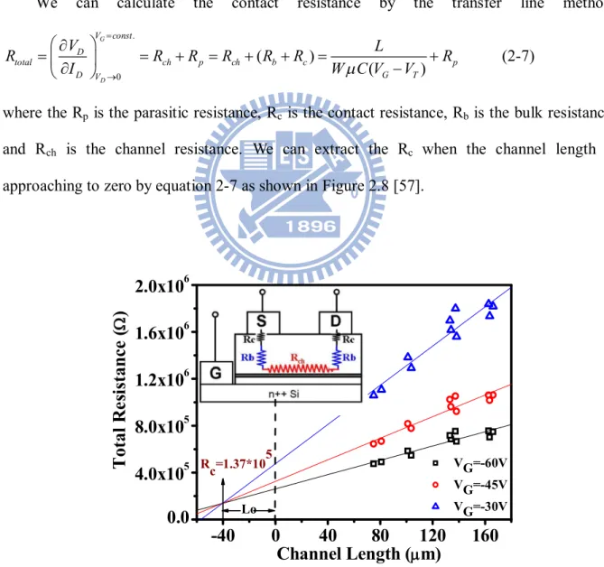
2.3.3 Contact resistance
There are two origins of the TFT series resistance: contact resistance and channel resistance. In recent years, researchers have pointed out that the performances of OTFTs are limited by the contact resistance at metal electrode/organic interface significantly [35-37, 57, 58]. The contact resistance has been found to be comparable with channel resistance. It implies us that the contact resistance plays an important role in determining the electrical characteristics.
We can calculate the contact resistance by the transfer line method:
. 0 ( ) ( ) G D V const D total ch p ch b c p D V G T V L R R R R R R R I W C V V (2-7)
where the Rp is the parasitic resistance, Rc is the contact resistance, Rb is the bulk resistance, and Rch is the channel resistance. We can extract the Rc when the channel length is approaching to zero by equation 2-7 as shown in Figure 2.8 [57].
-40
0
40
80
120
160
0.0
4.0x10
58.0x10
51.2x10
61.6x10
62.0x10
6Channel Length (m)
T
o
ta
l
R
e
si
st
a
n
ce
(
)
VG=-60V VG=-45V VG=-30V R c=1.37*10 5 LoChapter 3
Experimental and Analysis Methods
3.1 Substrate Preparation
3.1.1 Preface
The top-contact structure was chosen to fabricate the n-type OTFTs in this study due to its relatively better performance. The top-contact TFT is shown in Figure 2.1a. ITO (Indium Tin Oxide) is a kind of conducting material which also has high transparency. Because of that, ITO is always coated on glass substrate to form a conducting thin film. In this study, we choose ITO/glass and Si/SiO2 substrates. With the use of ITO/glass substrate, we usually need to define the ITO pattern by optical lithography. It is attributed to that the polymer insulator often provides a higher leakage current than SiO2 insulators due to its uniformity and compactness. The cleanness is also a important issue in fabricating OTFT devices. If the substrate is not clean, the uniformity of polymer layer will be low. We will introduce the cleaning process in the following section.
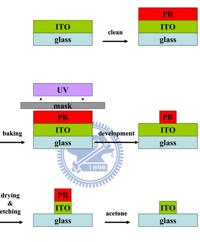
3.1.2 ITO Patterning Process
The process for ITO pattern is shown in Figure 3.1. First, we spin-coated a layer of photoresist (PR) on a cleaned ITO/glass substrate, and then we put shadow a mask that we designed for ITO pattern on the ITO/glass substrate followed by UV exposure for 100 seconds. Second, the exposure parts of PR would become soft and removed in development process. After development, HCl was used to remove the ITO which is with no PR. Finally, the hard PR is removed with acetone.
22
glass
glass
ITO
ITO
PR
clean
glass
ITO
PR
mask
UV
baking
glass
ITO
PR
drying
&
etching
glass
ITO
PR
development
glass
ITO
acetone
glass
glass
ITO
ITO
PR
clean
glass
ITO
PR
mask
UV
baking
glass
ITO
PR
drying
&
etching
glass
ITO
PR
development
glass
ITO
acetone
3.1.3 Cleaning of ITO/Glass Substrate
After etching of ITO, the glass substrates have to be completely cleaned. We washed the substrates with detergent first and rinsed by deionized water in the first place. The detergent can take the large particles and oil sludge away. The second step was soaking the substrates in acetone into an ultrasonic cleaner for 40 minutes. Organic pollutants would be swept away in this step. After rinsing by DI water in 5 minutes, we put the substrate in isopropyl alcohol (IPA) with ultrasonic microvibrations for 30 minutes. The residual acetone and water molecules would be taken away by IPA. Finally, we dried the substrates by nitrogen shower, and then these substrates are placed into an oven in which the temperature was set to 120°C for at least 24 hours to remove the water.
3.1.4 Cleaning of SiO
2/Si Substrate
We also use heavily doped n-type silicon wafers, with thermal SiO2 to fabricate the devices. The top SiO2 layer was 200 nm-thick, and the sheet resistance was about 0.001~0.003 ohm-cm. The capacitance per unit area in the SiO2 layer was 14.2 nF/cm2.
First, we put the substrates into a Teflon container, and rinsed them with DI water for 5 minutes. Then we dipped the container into a 3:1 mixture of concentrated sulfuric acid (H2SO4) and hydrogen peroxide (H2O2) at 80°C for 20 minutes. After this acid bath, we rinsed the substrates with DI water again for 5 minutes. Finally, we dried the substrates with nitrogen flow, and put them into a hot oven to remove the residual water.
24
3.2 The Materials
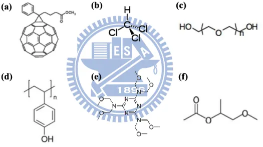
[6,6]-phenyl C61-butyric acid methyl ester (PCBM) [Figure 3.2(a)] was used as the active layer of the TFTs. We dissolved PCBM molecules in chloroform (CF) [Figure 3.2(b)]. The polymer poly(ethylene glycol) (PEG) [Figure 3.2(c)] has blended into the PCBM layer. The dielectric polymer film was made of poly(4-vinylphenol) (PVP) [Figure 3.2(d)] and poly(melamine-co-formaldehyde) methylated (PMCFM) [Figure 3.2(e)]; they were dissolved in propylene glycol monomethyl ether acetate (PGMEA) [Figure 3.2(f)].
The energy level diagram of the materials used in this study is displayed in Figure 3.3.
(a) (b) (c)
(d) (e) (f)
(a) (b) (c)
(d) (e) (f)
Figure 3.2 The structure of organic materials used in this experiments.
LUMO HOMO PCBM -3.7eV -6.1eV -4.2eV Al LUMO HOMO PCBM -3.7eV -6.1eV -4.2eV Al
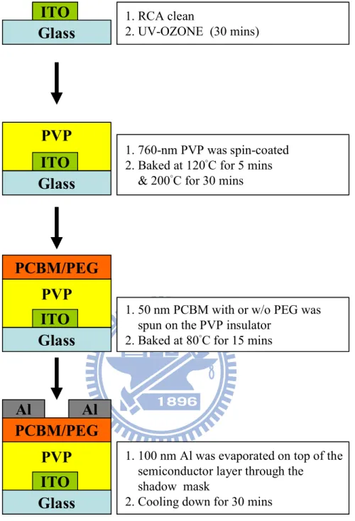
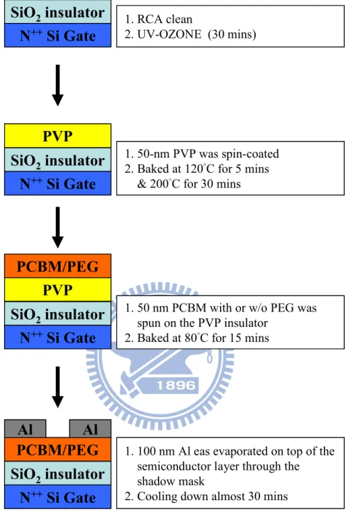
3.3 Device Fabrication Process of OTFTs
3.3.1 Spin-Coating Polymer Dielectric Film
The OTFT was fabricated on a ITO/glass substrate (<10 Ω/sq sheet resistance), where ITO was used as gate electrode. Before spin-casting of the polymer insulator, we put the substrates into an UV-Ozone machine for 30 minutes. The ozone molecules would burn the organic contaminant on substrates, and then be taken away by cleaning air flow.
The cleaned ITO substrates were then covered with a layer of 760-nm-thick polymer dielectric insulator, which was prepared by spin-coating of a solution of PVP (11wt%) and PMCFM (4wt%) (cross-linking agent) in PGMEA. The other OTFT was prepared on SiO2 substrate then covered with a layer of 50-nm-thick PVP interlayer.
The PVP films were firstly baked at 120°C for 5 minutes and then 200°C for 30minutes. The resulting capacitances per unit area of the insulator on ITO and the interlayer on SiO2 were 5.4 and 10.0 nF/cm2, respectively.
3.3.2 Spin-Coating of PCBM/PEG Blends as the Active Layer
and Evaporation of Metal Electrodes
The PCBM/PEG blended film was spin-coated on the PVP coated substrate inside a N2-filled glove box. The spin rate was set to 1000 r.p.m. for 30 seconds.
Before the deposition of S/D, the device was pre-annealed at 80°C for 15 min. Finally, Al was thermally evaporated onto the active layer under a pressure less then 5×10⁻⁶ torr through a shadow mask to form S/D contacts. The thickness of Al S/D was 100 nm. The channel length and width were 100nm and 2000μm, respectively.
26
PVP
ITO
Glass
ITO
Glass
PVP
ITO
Glass
PCBM/PEG
PVP
ITO
Glass
PCBM/PEG
Al
Al
1. 100 nm Al was evaporated on top of the semiconductor layer through the
shadow mask
2. Cooling down for 30 mins
1. 50 nm PCBM with or w/o PEG was spun on the PVP insulator
2. Baked at 80°C for 15 mins 1. 760-nm PVP was spin-coated 2. Baked at 120°C for 5 mins
& 200°C for 30 mins 1. RCA clean 2. UV-OZONE (30 mins)
PVP
ITO
Glass
ITO
Glass
PVP
ITO
Glass
PCBM/PEG
PVP
ITO
Glass
PCBM/PEG
Al
Al
1. 100 nm Al was evaporated on top of the semiconductor layer through the
shadow mask
2. Cooling down for 30 mins
1. 50 nm PCBM with or w/o PEG was spun on the PVP insulator
2. Baked at 80°C for 15 mins 1. 760-nm PVP was spin-coated 2. Baked at 120°C for 5 mins
& 200°C for 30 mins 1. RCA clean
2. UV-OZONE (30 mins)
SiO
2insulator
N
++Si Gate
SiO
2insulator
N
++Si Gate
PCBM/PEG
SiO
2insulator
N
++Si Gate
PCBM/PEG
Al
Al
PVP
SiO
2insulator
N
++Si Gate
PVP
1. RCA clean 2. UV-OZONE (30 mins) 1. 50-nm PVP was spin-coated 2. Baked at 120°C for 5 mins& 200°C for 30 mins
1. 50 nm PCBM with or w/o PEG was spun on the PVP insulator
2. Baked at 80°C for 15 mins
1. 100 nm Al eas evaporated on top of the semiconductor layer through the
shadow mask
2. Cooling down almost 30 mins
SiO
2insulator
N
++Si Gate
SiO
2insulator
N
++Si Gate
PCBM/PEG
SiO
2insulator
N
++Si Gate
PCBM/PEG
Al
Al
PVP
SiO
2insulator
N
++Si Gate
PVP
1. RCA clean 2. UV-OZONE (30 mins) 1. 50-nm PVP was spin-coated 2. Baked at 120°C for 5 mins& 200°C for 30 mins
1. 50 nm PCBM with or w/o PEG was spun on the PVP insulator
2. Baked at 80°C for 15 mins
1. 100 nm Al eas evaporated on top of the semiconductor layer through the
shadow mask
2. Cooling down almost 30 mins
28
3.4 Measurements and Analysis of OTFTs
3.4.1 Electrical Characteristics
In this work, we measured the electrical properties of the devices by Keithley 4200 IV measurement system at room temperature. For PCBM devices, we apply a positive gate voltage to accumulate electrons in the channel near the semiconductor/insulator interface. In the ID-VD measurement, we swept the gate bias from 0 to 60V, and the gate voltage step was 15 V from VG = 0 V to VG = 60 V. Additionally, in the ID-VG measurement, we swept the drain voltage from -20 V to 60 V, and the drain voltage step was from 15V to 60V.
3.4.2 Capacitance Analysis
We measured the capacitances of SiO2 and PVP cross-linked polymer by HP 4284A using metal-insulator-metal (MIM) structure.
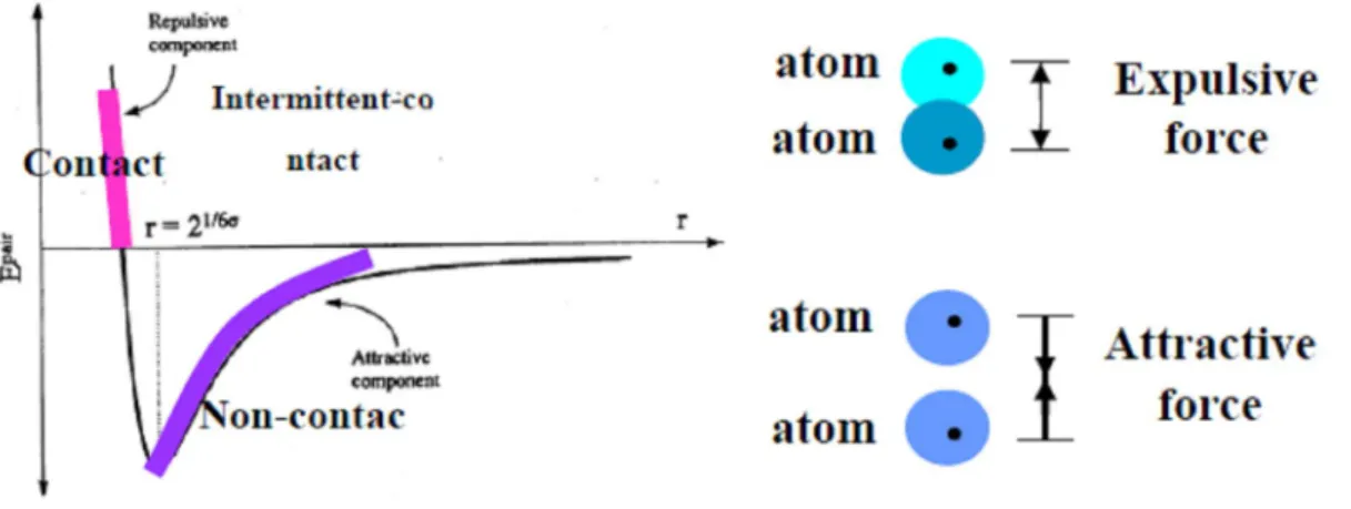
3.4.3 Surface Morphology Measurement
The atomic force microscope (AFM) has been invented in 1985, which could measure the surface morphology of low conductivity materials. The principle of AFM is the interaction of van der Waals force, which is different with scanning electron microscope (SEM) by electron tunneling effect. We assume there are two atoms: one is on the tip of the cantilever, the other is on the surface of sample. The interaction force between the two atoms depends on their distance as show in Figure 3.6. In this study, we used Digital Instruments Dimension 3100 AFM to get the surface morphology of the active layer. Figure 3.7 shows how can AFM work to obtain surface properties.
Figure 3.6 The interaction force between two atoms.
30
3.4.4 X-ray Photoelectron Spectroscopy Measurement
X-ray photoelectron spectroscopy (XPS) is a quantitative spectroscopic technique that measures the elemental composition, chemical state and electron state of the elements that exist in materials. The basic components of XPS system is shown in Figure 3.8. XPS spectra are obtained by irradiating a material with a beam of X-rays while measuring the kinetic energy and number of electrons that escape from the top thin-film (1 to 10 nm) of the material being analyzed simultaneously. XPS requires ultra high vacuum (UHV) conditions. XPS detects all elements with an atomic number (Z) of 3 (lithium) and above. It cannot detect hydrogen (Z = 1) or helium (Z = 2). XPS is routinely used to analyze inorganic compounds, metal alloys, semiconductors, polymers, catalysts, glasses, make-up, teeth, bones, and many others.
From XPS measurement, we can know if there is any chemical interaction between PEG and Al S/D electrodes. In 2006, Guo et al. reported that the performances of polymer light-emitting diodes could be improved by the formation of a PEGDE (PEG dimethyl ether)/Al complex at the cathode interface [58]. In Figure 3.9, the C1s XPS spectrum of the HY-PPV/Al has a main peak at a binding energy 284.6 eV. The peak is associated with hydrocarbon atoms. When an additional PEGDE modify layer (2.5 nm) was inserted on the surface of the HY-PPV layer with Al, the C1s peak at 288.6 eV grew. PEGDE is a polymer with the same sequent carbon-oxide functional group like PEG, (-CH2CH2O-)n, so a chemical reaction between the lone-pair electrons and Al in the oxygen atoms of the PEGDE chains was expected. The C1s diagram at 288.6 eV is related to the formation of the organic oxide/Al complex. Due the former results, we expect that PEG would react with Al and we can get the information from the XPS measurement.
Figure 3.8 Basic components of monochromatic XPS system.
[Adapted from http://en.wikipedia.org/wiki/X-ray_photoelectron_spectroscopy ]
Figure 3.9 XPS C1s spectra of pristine HY-PPV (◇), HY-PPV / Al (●), and HY-PPV / PEGDE / Al [58].
32
Chapter 4
Results and Discussion
4.1 Characteristics of Device Electrical Properties
4.1.1
The Effect of Molecular Weight of PEG
We measured these devices prepared with various molecular weight of PEG in a N2-filled glove box, where the concentrations of O2 and H2O were less than 1 ppm. Figure 4.1 illustrates the ID-VD electrical properties of these devices. Figure 4.1(a) shows the characteristic of pristine 1wt% PCBM device. From 4.1(b)-(f) represent the devices prepared whose molecular weight (M.W.) was with PEG 400, 1000, 3000, 8000, and 20000, respectively. All the weight ratio of PEG:PCBM is 1:20. The device with pristine PCBM has the lowest drain current in the saturation regime, and the device prepared with PEG 20000, meaning the M.W. was 20000 had a three-times higher drain current than that of pristine PCBM TFT. We can find that when the larger molecular weight of PEG blending, we could get higher drain current.
The ID-VG characteristics are shown as Figure 4.2. The data shown in Figure 4.2 were measured at VD = 60V and VG was swept from -20 to 60 V. Furthermore, the electron mobility was calculated from slopes of square root of drain current versus gate voltage in the saturation regime [Figure 4.2(b)]; the important electrical characteristic parameters were summarized in Table 4.1. The device prepared with PEG 20000 had higher on-off current ratio (4.1×10⁴), and exhibited a showed lower threshold voltage (-2.61V). The mobility (0.0440 cm2/Vs) also became three times larger then that of pristine device (0.0141 cm2/Vs). The value of electron mobility is comparable with that of the device made with a Cs2CO3 buffer layer on Al electrodes (0.0445 cm2/Vs) [37].
0 10 20 30 40 50 60 0.0 0.5 1.0 1.5 2.0
a
0.65 ID (u A) VD (V) VG= 0V VG=15V VG=30V VG=45V VG=60V 0 10 20 30 40 50 60 0.0 0.5 1.0 1.5 2.0b
1.07 ID ( u A ) VD (V) 0 10 20 30 40 50 60 0.0 0.5 1.0 1.5 2.0c
1.22 ID ( u A ) VD (V) 0 10 20 30 40 50 60 0.0 0.5 1.0 1.5 2.0d
1.32 ID ( u A ) VD (V) 0 10 20 30 40 50 60 0.0 0.5 1.0 1.5 2.0e
1.90 ID ( u A ) VD (V) 0 10 20 30 40 50 60 0.0 0.5 1.0 1.5 2.0f
2.00 ID ( u A ) VD (V)Figure 4.1 The ID-VD output curves of (a) pure PCBM device, and device prepared with PEG (b) 400, (c) 1000, (d) 3000, (e) 8000, and (f) 20000, respectively.
34 -20 0 20 40 60 10-11 10-10 10-9 10-8 10-7 10-6 pure 200 400 600 1000 1500 3000 8000 20000
a
ID ( A ) VG (V) -20 0 20 40 60 0.0 5.0x10⁻⁴ 1.0x10⁻³ 1.5x10⁻³b
[I D ] 0 .5 ( [A ] 0 .5 ) VG (V)Figure 4.2 The (a) ID-VG and (b) ID1/2-VG transfer curves at VD =60V with distinct molecular weight of PEG blending.
Table 4.1 The parameters of the OTFTs with distinct PEG molecular weight (MW) blending measured in nitrogen filled glove box.
MW of PEG (g/mol) Mobility (cm2/Vs) VT (V) On-off ratio Pure PCBM 0.0141 17.02 0.6×10⁴ 200 0.0145 4.78 1.2×10⁴ 400 0.0215 0.84 1.4×10⁴ 600 0.0245 -0.56 1.1×10⁴ 1000 0.0264 -0.74 1.2×10⁴ 3000 0.0285 -0.20 1.1×10⁴ 8000 0.0376 -0.90 2.0×10⁴ 20000 0.0440 -2.61 4.1×10⁴
4.1.2
The Effect of PEG Concentration
In this section, the effect of PEG concentration is investigated. Figure 4.3 illustrates the ID-VD electrical performances of different devices. Figure 4.3(a) shows the characteristic of pure-PCBM device. Figure 4.3(b) to 4.3(f) represent the output curves of the devices prepared with 1%, 5%, 8%, 11% and 16% PEG (M.W.=20000), respectively. From the figures, we can find that the saturation drain current increased with increasing PEG concentration. However, while the weight ratio of PEG excess 5 wt%, the value of saturation drain current became lower as shown from Figure 4.3(d) to 4.3(f).
The ID-VG transfer characteristics are shown in Figure 4.4. All the devices were measured at VD = 60 V and VG bias was swept from -20 V to 60 V. The threshold voltage extracted from square root of drain current versus VG shifts negatively due to the higher ratio of PEG blending. The device with 5% PEG 20000 blending shows the best electrical performance. The other important electrical characteristic parameters were shown in Table 4.2.
36 0 10 20 30 40 50 60 0.0 0.5 1.0 1.5 2.0
0%
a
0.65 ID ( u A ) VD (V) VG= 0V VG=15V VG=30V VG=45V VG=60V 0 10 20 30 40 50 60 0.0 0.5 1.0 1.5 2.01%
b
1.26 ID ( u A ) VD (V) 0 10 20 30 40 50 60 0.0 0.5 1.0 1.5 2.05%
c
2.00
ID ( u A ) VD (V) 0 10 20 30 40 50 60 0.0 0.5 1.0 1.5 2.08%
d
1.11 ID ( u A ) VD (V) 0 10 20 30 40 50 60 0.0 0.5 1.0 1.5 2.011%
e
0.32 ID ( u A ) VD (V) 0 10 20 30 40 50 60 0.0 0.5 1.0 1.5 2.016%
f
0.14 ID ( u A ) VD (V)Figure 4.3 The ID-VD output curves of (a) pure PCBM OTFTs, and with (b) 1%, (c) 5%, (d) 8%, (e) 11%, and (f) 16% PEG 20000 blending, respectively.
-20 0 20 40 60 10-11 1x10⁻¹⁰ 1x10⁻⁹ 1x10⁻⁸ 1x10⁻⁷ 1x10⁻⁶
a
ID (A) VG (V) Pure 1% 5% 8% 11% 16% -20 0 20 40 60 0.0 2.0x10⁻⁴ 4.0x10⁻⁴ 6.0x10⁻⁴ 8.0x10⁻⁴ 1.0x10⁻³ 1.2x10⁻³ 1.4x10⁻³ 1.6x10⁻³b
[I D ] 0 .5 ( [A ] 0 .5 ) VG (V)Figure 4.4 The (a) ID-VG and (b) ID1/2-VG transfer curves at VD =60V with distinct concentration of PEG 20000 blending.
Table 4.2 The parameters of the OTFTs with different ratio PEG 20000 blending measured in nitrogen filled glove box.
Weight ratio of PEG (wt%) Mobility (cm2/Vs) VT (V) On-off ratio Pure PCBM 0.0141 17.02 0.6×10⁴ 1 0.0241 6.13 1.3x10⁴ 5 0.0440 -2.61 4.1x10⁴ 8 0.0211 -3.54 1.2x10⁴ 11 0.0098 -14.19 0.8x10⁴ 16 0.0014 -14.21 1.5x10⁴
38
4.1.3
The Electrical Characteristics Measured in the Atmosphere
We try to measure these devices in ambient environment in which the relative humidity was about 60%. Figure 4.5 illustrate the ID-VD electrical output performances prepared without [Figure 4.5(a)] and with [Figure 4.5(b)] PEG 1500. The device with PEG1500 (5%) blending had much higher saturation drain current.
0 10 20 30 40 50 60 0 20 40 60 80 100 120
a
ID ( n A ) VD (V) VG= 0V VG=15V VG=30V VG=45V VG=60V 0 10 20 30 40 50 60 0 20 40 60 80 100 120b
ID ( n A ) VD (V)Figure 4.5 The ID-VD output curves of the OTFTs (a) without and (b) with PEG 1500 (5%) blending in the ambient environment.
Table 4.3 The comparison of transfer characteristics of the OTFTs measured in inert and ambient environment. Mobility (cm2/Vs) VT (V) On-off ratio Pure (inert) 1.41×10⁻² 17.02 0.6×10⁴ Pure (ambient) 3.19×10⁻⁵ 23.35 0.05×10⁴ PEG (inert) 2.64×10⁻² -0.74 1.2×10⁴ PEG (ambient) 2.04×10⁻³ 18.58 0.2×10⁴
Figure 4.6 shows the ID-VG transfer output performance and it suggests that the pure-PCBM OTFT showed a poor and unstable electrical characteristic in the ambient environment. On the other hand, the device with PEG shows a relatively higher drain current although it was still prepared lower than that of the device measured in an inert environment. Table 4.3 summarizes the transfer performances of these devices in the ambient atmosphere. For the device prepared without PEG, the threshold voltage shifted from 17.02 to 23.35 V and the mobility decreased from 1.4×10⁻² to 3.2×10⁻⁵ cm2/Vs. After the addition of PEG, the threshold voltage shifted from -0.74 to 18.58 V and the mobility decreased from 2.6×10⁻² to 2.0×10⁻³ cm2/Vs. The mobility of the pristine PCBM device encountered three order decay; but the mobility of PEG 1500 device decayed by just one order of magnitude. Even though the performance measured in the ambient environment was still decayed, PEG blending in active layer might be a good method to protect the channel.
-20 -10
0
10 20 30 40
10
-1210
-111x10
-101x10
-91x10
-8a
ID
(
A
)
VG (V)
-20 -10
0
10 20 30 40
0.0
5.0x10
-51.0x10
-41.5x10
-42.0x10
-4b
[I
D
]
0 .5([
A
]
0 .5)
VG (V)
V D=30V Pure PCBM V D=60V Pure PCBM V D=30V PEG 5% V D=60V PEG 5%Figure 4.6 The (a) ID-VG and (b) ID1/2-VG transfer curves at VD = 30 V and 60 V of the OTFTs with and without PEG blending in ambient environment.
40
4.1.4
The Effect of PEG on the Devices Fabricated on PVP/SiO
2Substrate
We measured the devices prepared with PCBM/PEG 400 composition fabricated on PVP/SiO2 substrates. Figure 4.7 illustrates the ID-VD electrical performances measured in inert environment. The device with pristine-PCBM has lower drain current in the saturation regime. The device with PEG blending has two times higher drain current than that of pristine-PCBM OTFT. The data shown in Figure 4.8 were measured at VD = 60 V, and VG bias swept from -20 to 60 V. The device prepared with PEG 400 had higher on-off current ratio (9.0×10³), and then showed large threshold voltage shift (from 31 V to 5 V). The other important extracted parameters were summarized in Table 4.4.
0 10 20 30 40 50 60 0.0 0.1 0.2 0.3 0.4 0.5 0.6 0.7
a
ID ( A ) VD (V) VG= 0V VG=15V VG=30V VG=45V VG=60V 0 10 20 30 40 50 60 0.0 0.1 0.2 0.3 0.4 0.5 0.6 0.7b
ID ( A ) VD (V)Figure 4.7 The ID-VD output curves of the OTFTs prepared (a) without, and (b) with PEG 400 on PVP/SiO2 substrates.
![Figure 2.2 The structure of polarons. [Adapted from http://upload.wikimedia.org/ wikipedia/commons/d/d0/Polaron]](https://thumb-ap.123doks.com/thumbv2/9libinfo/8128321.166143/22.892.194.784.327.718/figure-structure-polarons-adapted-wikimedia-wikipedia-commons-polaron.webp)
![Figure 2.3 The origin of polaron in energy band [8].](https://thumb-ap.123doks.com/thumbv2/9libinfo/8128321.166143/23.892.167.764.115.393/figure-origin-polaron-energy-band.webp)
![Figure 3.9 XPS C1s spectra of pristine HY-PPV (◇), HY-PPV / Al (●), and HY-PPV / PEGDE / Al [58]](https://thumb-ap.123doks.com/thumbv2/9libinfo/8128321.166143/41.892.266.666.514.810/figure-xps-spectra-pristine-ppv-ppv-ppv-pegde.webp)
