國 立 交 通 大 學
顯 示 科 技 研 究 所
碩 士 論 文
不同氧化銦錫結構應用於氮化鎵垂直共振腔面射型雷射之研究
Study of GaN-based VCSELs with different ITO layer structure
研
研
究
究
生
生
:
:
陳
陳
建
建
綱
綱
..指
指
導
導
教
教
授
授
:
:
郭
郭
浩
浩
中
中
教
教
授
授
盧
盧
廷
廷
昌
昌
教
教
授
授
不同氧化銦錫結構應用於氮化鎵垂直共振腔面射型雷射之研究
Study of GaN-based VCSELs with different ITO layer structure
研 究 生:陳建綱 Student:Chien-Kang Chen
指導教授:郭浩中 Advisors:Hao-Chung Kuo
盧
盧
廷
廷
昌
昌
Tien-Chang Lu
國 立 交 通 大 學
顯 示 科 技 研 究
所
碩 士 論 文
A ThesisSubmitted to Display Institute
College of Electrical Engineering and Computer Science National Chiao Tung University
in partial Fulfillment of the Requirements for the Degree of Master
in
Display Institute July 2009
不同氧化銦錫結構應用於氮化鎵垂直共振腔面射型雷射
之研究
研究生:陳建綱 指導老師:盧廷昌老師 郭浩中老師 國立交通大學 顯示科技研究所摘要
本篇論文是在電機發混合式氮化鎵垂直共振腔雷射結構中,以30奈米厚度取代 舊有一光學波長厚度的氧化銦錫層並探討其光性與電性的改善。首先,我們使用 模擬軟體模擬不同厚度的氧化銦錫層對共振腔Q值的影響,由模擬的結果可知在 沒有氧化銦錫層和有210奈米的氧化銦錫層的共振腔中Q值分別為3300及700;若 換成30奈米厚,Q值僅會減少至3100,由此我們可預期用薄的氧化銦錫層能有效 的提升共振腔的Q值。接著,在實驗中我們使用了四種不同元件的透明導電層, 分別使用電子槍蒸鍍的30奈米與210奈米氧化銦錫層,還有利用離子濺鍍的30奈 米結晶性和10奈米非晶性+20奈米結晶性氧化銦錫層。經由量測結果,30奈米厚 的元件Q值約為1600,比起210奈米厚度的氧化銦錫層元件700高出了兩倍多。這 樣的結果已能達到我們希望利用薄的氧化銦錫層去減少共振腔內光學損耗的目 的。最後再比較四種氧化銦錫層應用於元件的特性。實驗結果顯示10奈米非晶性 +20奈米結晶性氧化銦錫層的元件不僅具有最低的串聯電阻(165Ω)等電性表現 外,其發光強度在電流孔徑所佔的比例更高達94%,此結果說明大部分的激發光 都被侷限在設計的共振腔中,如此便能有效的降低產生雷射的臨界條件。在本論 文中,我們不僅證實薄的氧化銦錫層可以有效提高元件的Q值,並且也找到一種 最符合的氧化銦錫結構應用於我們的電機發面射型雷射上。Study of GaN-based VCSEL with different ITO structure
Student : Chien Kang Chen Advisor : Dr. T.C. Lu Dr. H.C. Kuo Institute of display institute National Chiao-Tung University
Abstract
We have investigated the electrical and optical performance of GaN-based VCSELs with hybrid mirrors by four different ITO structures, especially in 30nm ITO layer instead of the traditional ITO layer of about 1λ thickness. First, by the simulation results, the qualify factors of the samples without ITO layer and with 210nm ITO layer were 3300 and 700, respectively. However, the sample with 30nm ITO layer was slightly decreased to 3100. It represents the thinner ITO layer can increase the qualify factor and reduce the internal loss of the cavity caused by the ITO layer in our devices. Then, we used four different ITO structures in our VCSELs including 30nm ITO film by e-gun, 210nm ITO film by e-gun, 30nm ITO film by sputter, and 10nm amorphous(α)-ITO film plus 20nm ITO film by sputter. Compared the VCSELs with four different ITO structures, the devices with 10nmα-ITO film plus 20nm ITO film by sputter has the lower serious resistance of about 165Ω and better optical confinement of about 94% in the aperture, and the quality factor of devices with 30nm ITO also has the higher quality factor of 1600. By the results, we can efficiently decrease the lasing threshold condition in our devices. In the report, we can not only increase the qualify factor but also obtain a better ITO structure used in our VCSELs. Finally, the VCSELs have the great potential to be the first electrical
誌謝
歲月如梭,很快地碩班的兩年就這樣過去了。想當初在大學時由於修了郭 老師的課,才開始對光電顯示的領域產生了興趣,也因此後來才會選擇申請顯示 所並有幸加入半導體雷射實驗室這個大家庭。實驗室的三位老師,王老師雖然跟 我們碩士班的學生接觸較少,不過王老師對於學術的熱忱與活力以及待人的赤子 之心,都相當的值得我們這些晚輩去效法。而郭老師除了是介紹我進入實驗室的 領路人外,也感謝郭老師空閒的時候對我們生活上的關心。至於盧老師則是我的 主要的論文指導老師,很感激盧老師平日在我實驗與研究上的指導,雖然我在理 論部分的基礎仍稍嫌薄弱,且表達的方式也一直不是很有自信。可是盧老師仍常 不厭其煩的聆聽我的問題並給予適當的建議。Tiger team的直屬學長宗鼎、士偉 和子維是我在碩班生活中的指導者也是我做實驗時最強力的後盾,實驗上常會遭 遇到許多無法預料的問題,這種時候就往往需要學長的幫忙才得以順利度過。另 外,也要感謝李博、明華與AOT的學長,如果沒有你們磊晶的支持,我做的製程 部分很難會有現在的表現與突破。清華和柏孝學長則常給我在製程與儀器方面的 協助與意見。而至於關於ITO鍍膜的部分要感謝逸駿學長與佳能安內華公司對我 在這方面的協助,這個部分是我這次論文中很重要的一環。此外也滿感謝跟著我 一同進入實驗室一起打拼的同學們:玫君、小馬、QQ、啄木、治凱、小柯、董 ㄟ、生哥和尚樺,謝謝你們不僅在實驗上對我的幫助,在生活上也帶著我一起玩 樂讓我能夠開心的度過這充實的兩年時光。未來即使大家又再度分處不同的城市 有著不一樣的發展,希望大家日後還是能保持聯絡喔。接著還要感謝實驗室學弟 妹們,直屬的哭哭、阿祥和嗡嗡嗡,相信你們經過一年的學習後,都會有青出於 藍比我更好的表現。還有智維與詳淇,在我碩二的後期很謝謝你們在我穿透率nk 與模擬方面的協助,才使得我的論文能夠更加的完整。最後也要感謝我的家人, 雖然我不常回家去探望你們,但你們還是常會主動打電話來關心我,傾聽我在實 驗或生活上的種種抱怨,希望我的表現不會令你們失望。 2009/07/27 建綱于Contents
Abstract (in Chinese)...i
Abstract (in English)...ii
Acknowledgement……….iii
Contents...iv
Figure Contents...vii
Table Contents…….………..………....x
Chapter 1 Introduction………..1
1.1 Wide band gap Ⅲ-Ⅴ materials……….1
1.2 Nitride-based semiconductor lasers………...3
1.2.1 Edge emitting lasers………...3
1.2.2 Vertical Surface Emitting Lasers………..6
Ⅰ. Fully epitaxial grown VCSEL structure………8
Ⅱ. VCSEL structure with two dielectric mirrors….8 Ⅲ. VCSEL structure with hybrid mirrors……….9
1.3 The main challenges for electrically pumped GaN-based VCSELs……….13
1.4 Outline of the thesis………15
Chapter 2 Motivation……….16
2.1.1 Optical pumped VCSELs…….………16
2.1.2 CW lasing of current injected GaN-based VCSEL at 7 7 k … … … 1 9 2.2 Reflectance spectra simulation………..23
Chapter 3 Characteristics of an Optical Pumped GaN-Based VCSELs…....27
3.1 Optical measurement system………..27
3.2 Fabrication and characteristics of optical pumped VCSELs…...29
Chapter 4 Characteristics and measurement of indium-tin-oxide……...…..35
4.1 Introduction to indium-tin-oxide………35
4.1.1 Transparent conduct layer (TCL)……….35
4.1.2 Characteristics of ITO………..…….36
4.2 Measurement method and equipments………38
4.2.1 Scanning electron microscopy (SEM)…………...….38
4.2.2 Four point probe………..………..40
4 . 2 . 3 C i r c u l a r Tr a n s m i s s i o n L i n e M o d e l ( C T L M ) measurement………..……….41
4.3 Result and discussion………44
4.3.1 Specific contact resistance………..44
4.3.2 ITO surface morphology………..46
4.3.3 Refractive index and extinction coefficient…..50
VCSELs……….…………55
5.1 GaN-based VCSELs process………...………55
6.1.1 Initial clean and photolithography technique…….55
6.1.2 Process flowchart……….…………57
5.2 The electroluminescence (EL) measurement system…………..61
5.3 The characteristics of Ga N-ba sed VCSEL at Roo m temperature……….63
5.3.1 VCSEL devices with 210nm ITO deposited by E-gun e v a p o r a t i o n … … … . … . . … … … … . … . 6 3 5.3.2 VCSEL devices with 30nm ITO deposited by E-gun evaporation………..……….….66
5.3.3 VCSEL devices with 30nm crystalline ITO deposited by sputter………..……….….69
5.3.4 VCSEL devices with 10nmα+20nm crystalline ITO deposited by sputter………..……….….71
5.3.5 The reliably of GaN-based VCSEL with different ITO TCL……….73
5.4 Summary……….……….………..75
Chapter 6 Conclusions and future work……….………..77
6.1 Conclusions……….………...…………...………77
6.2 Future work……….………...…………...………79
Figure Contents
Fig 1.1 the band-gap diagram of Ⅱ-Ⅵ and Ⅲ-Ⅴ group semiconductor material...2 Fig 1.2 the schematic diagram of the edge emitting laser diode……….5 Fig 1.3 the schematic diagram of the VCSELs…………..………..……….7 Fig 1.4 the schematic diagram of three nitride based VCSELs structures…..…12 Fig 2.1 the schematic diagram of the optical pumped VCSEL structure…..…..17 Fig 2.2 PL emission of the optical pumped VCSEL structure………..…17 Fig 2.3 the excitation energy - emission intensity curve (L-I)……….18 Fig 2.4 the laser emission spectrum with the increasing pumping energy……...18 Fig 2.5 the schematic diagram of the current injected VCSEL structure…………20 Fig 2.6 the emission spectrum of the current injected VCSEL structure...…..21 Fig2.7 the light output intensity vs injection current and current–voltage
characteristics of GaN VCSEL………...21 Fig 2.8 the laser emission spectrum at different injection current levels measured at 77 K…..….……….………..22 Fig 2.9 the cavity structure of simulation………..………..24 Fig 2.10 the simulated reflectance spectra with different thickness of ITO……….25 Fig 2.11 the simulated cavity mode with different thickness of ITO…………...….25 Fig 2.12 the simulated quality factor with different thickness of ITO………..……26 Fig 3.1 the setup of optical measurement system………..28 Fig 3.2 The schematic diagram of the optical pumped VCSEL structure…………31 Fig 3.3 The reflectance spectrum of bottom DBR………31
Fig 3.5 the PL and reflectance spectrum of VCSEL without upper DBR………….32
Fig3.6 The reflectance spectrum of upper DBR………..……….……33
Fig 3.7 The PL spectrum of optical pumped VCSEL with upper DBR………33
Fig 3.8 The pumping energy density versus normalized intensity diagram………..34
Fig 3.9 The lasing spectrum of optical pumping VCSEL……….34
Fig 4.1 the scanning electron microscopy (SEM) system of our lab………….…...39
Fig 4.2 Schematic of 4-point probe configuration………...40
Fig 4.3 four point probe in NCTU Nano Facility Center……….41
Fig 4.4 the ITO CTLM pattern after etching……….43
Fig 4.5 the schematic diagram of total resistance versus gap distance ………44
Fig 4.6 ITO specific contact resistance (a)with different annealing time and(b) with d i f f e r e n t a n n e a l i n g t e mp e r a t u r e … … … . . … … … . 4 5 Fig 4.7 (a) sputter 150℃ crystalline 30nm ITO (b) sputter 10nm amorphous + 20nm crystalline ITO……….47
Fig 4.7 (c) E-gun 30nmITO (d) E-gun 210nm ITO……….49
Fig 4.8 the refractive index and extinction coefficient versus wavelength diagram for sputter (a) 30nm crystalline ITO (b) 10nm α+ 20nm crystalline ITO...51
Fig 4.8 the refractive index and extinction coefficient versus wavelength diagram for E-gun (c) 30nm ITO (d) 210nm ITO……….52
Fig 5.1 The schematic diagram of overall VCSELs process flowchart………58
Fig 5.2 The defined mesa of first step was measured by probe station………59
Fig 5.3 The ITO transparent conduct layer deposited on current aperture……...59
Fig 5.4 The schematic diagram of completed electrical pumped VCSEL………...60
Fig 5.6 The EL measurement system of electrically driven VCSELs………...62 Fig5.7 The previous electrically characteristics of VCSEL device with 240nm
ITO………64 Fig 5.8 (a) LIV curve and (b) optical intensity distribution of VCSEL with 210nm
ITO……….65 Fig 5.9 The EL spectrum of VCSEL device with 210nm ITO, and the inset figure is the CCD image of the current aperture……….66 Fig 5.10 (a) LIV curve and (b) optical intensity distribution of VCSEL with 30nm ITO deposited by E-gun………..68 Fig 5.11 The EL spectrum of VCSEL device with 30nm ITO deposited by E-gun , and the inset figure is the CCD image of the current aperture………….….68 Fig 5.12 (a)LIV curve and (b) optical intensity distribution of VCSEL with
crystalline 30nm ITO deposited by sputter………70 Fig 5.13 The EL spectrum of VCSEL device with crystalline 30nm ITO deposited by sputter, and the inset figure is the CCD image of the current aperture.70 Fig 5.14 (a) LIV curve and (b) optical intensity distribution of VCSEL with 10nmα +20nm crystalline ITO deposited by sputter………72 Fig 5.15 The EL spectrum of VCSEL device with 10nmα+20nm crystalline ITO deposited by sputter, and the inset figure is the CCD image of the current aperture………..……….73 Fig 5.16 Voltage and output power versus current density diagram of VCSEL with different ITO structures……….…..74 Fig 6.1 (a) the devices with AlN current blocking layer (b) the devices with ions implantation……….79
Table Contents
Table 4.1 the characteristics comparison of four different ITO thin film……….…54 Table 5.1 The overall electrical and optical characteristics of GaN-based VCSEL
with four different ITO structures………..76
Chapter 1
Introduction
1.1 Wide-bandgap III-V materials
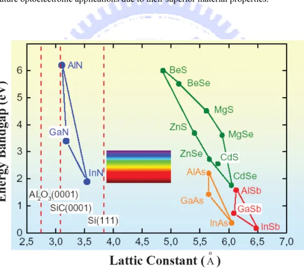
Wide-bandgap nitride materials have attracted great attention over past decade due to their promising potential for the applications of optoelectronic devices such as flat panel display, competing storage technologies, automobiles, general lighting, and biotechnology, and so on [1-4]. The III-N materials are synthesized mainly using the
four kinds of atoms, gallium (Ga), nitride (N), aluminum (Al), and indium (In), to form the binary and ternary compounds such as GaN, InN, AlN, InxGa1-xN, and AlxGa1-xN etc. The bandgap of these materials cover a very wide range from 0.9eV to 6.1eV (figure 1.1), which implies the large band off-set in hetero-structure could be achieved in this material system. The large band off-set is very useful to confine carrier for the high-speed and high power electronic devices and light emitting devices [5]. Their wide-range bandgap also provide possibility of full-color emission
because they cover red, green, and blue emission regions. This property further makes nitride materials important and important for the applications of full-color display or solid-state lighting. Furthermore, nitride materials still have lots of advantages such as
high bond energy (~2.3eV), high saturation velocity (~2.7 × 104 cm/s), high
breakdown field (~2 × 10⁶ V/cm), and strong excitonic energy (>50meV)[6-7].
Although wurtzite nitride compounds have some unique properties such as piezoelectric field and spontaneous polarization which is harmful to the efficiency of light emitting devices, the material system still is a very strong candidate for the future optoelectronic applications due to their superior material properties.
1.2 Nitride-based semiconductor lasers
The research of blue light emitting devices began from the development of gallium nitride light emitting diodes in the early 1970s[8-10]. Two decades later, with
several efforts devoted to the growth of nitride materials, doping concentration, efficiency of quantum wells, and so on, Nakamura et. al. [2] developed the first
prototype high-brightness (>100 times greater than previous alternatives, about 1 candela) GaN blue light emitting diodes in 1993. Then, in 1995, they also developed the first successful GaN electron-injection laser [1]. This makes nitride laser diodes
begin to step on the road toward the commercial applications of high-information-density storage, laser printer, compact projector, and etc. In these years, the performance of nitride laser diodes has been improved to emit power as high as 100mW at room temperature with a low threshold only 3 kA/cm2 [11], and the devices have been already successfully commercialized to be applied to digital versatile disc (DVD). This next-generation DVD would enlarge the storage capacity from 4.7 giga-bytes which current DVD owns to 27 giga-bytes.
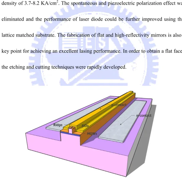
1.2.1 Edge emitting lasers
This kind of structure is currently the most mature and producible one among all nitride laser devices. It is featured by a stripe-type long cavity and a pair of cleaved facet as the mirrors as shown in figure 1.2. Typically, the cavity length of the structure is about several hundred micro-meters. The light in the cavity is resonant in the horizontal direction and emits from the cleaved mirrors. The standard epi-layer structure of EELs usually is grown on sapphire and composes of p-n junction, multiple quantum wells (active region), and some cladding layer for photons and electrons. Over this decade, several improvements and researches on the growth and optimization of its structure were reported[12-15]. One is to improve the great amounts
of defects and threading dislocations existing in the grown nitride materials on sapphire substrate due to the large lattice-mismatch between the nitride material and sapphire. The epitaxally lateral overgrowth (ELOG) is a very efficient method to reduce threading dislocation and defect density [12, 13]. It is a method using the
patterned SiOx to make GaN laterally coalesce and bend threading dislocations to reduce the dislocation density. Generally, ELOG could decrease dislocation density down to the order of 108cm-2. Other one is to raise the low confinement factor of the
optical field in the structure. Because the index difference between AlxGa1-xN and
et. al. provided a solution that using modulation doped strain superlattice layer to improve the optical confinement [12, 13]. The other is to reduce spontaneous
polarization and piezoelectric field in multiple quantum wells. Recently, M. Schmidt et. al. [14]and D. Feezell [15]et. al. demonstrated nonpolar laser diode on m-plane GaN
substrate. The laser diode emits violet light ~410nm and has the threshold current density of 3.7-8.2 KA/cm2. The spontaneous and piezoelectric polarization effect was
eliminated and the performance of laser diode could be further improved using this lattice matched substrate. The fabrication of flat and high-reflectivity mirrors is also a key point for achieving an excellent lasing performance. In order to obtain a flat facet, the etching and cutting techniques were rapidly developed.
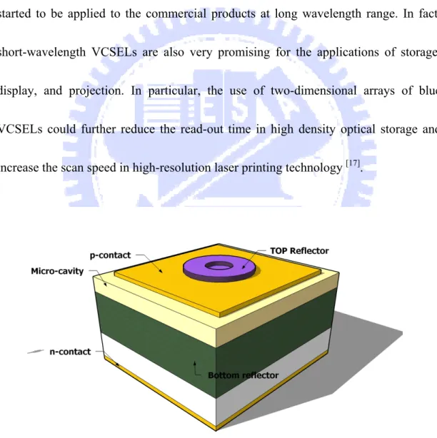
1.2.2 Vertical Surface Emitting Lasers
Although the optimization of the edge emitting laser keeps going, some properties of this kind of laser are unfavorable. One of those properties is its elliptic beam shape. On one hand, the coupling efficiency would be low as the elliptic beam is coupled into optical fiber (typically in the form of circular core). On the other hand, for the application of storage, the elliptic beam not only makes each writing pixel larger but also raises expenses for correcting light shape. Usually, this kind of laser shows slightly large divergence angle to be over ten degree. This also is disadvantageous to the projection. Furthermore, the side emitting laser devices also makes the testing of devices a tough task. The wafer should be cut into several stripes (several laser devices on one strip) before the testing. For a commercial product, the complicated testing would result in a poor producing efficiency and be disadvantageous. Therefore, in order to have a superior laser device, K. Iga [16]
demonstrated a new kind of laser diodes, vertical cavity surface emitting laser, in 1977. Vertical cavity surface emitting laser (VCSEL) is a vertical-emitting-type laser. It is formed by sandwiching a few-lambda cavity in a pair of reflectors, usually in the form of distributed Bragg reflector (DBR), with a very high reflectivity (>99.9%) (as shown in figure 1.3). In contrast to EELs, photons in the cavity of
VCSEL are vertically in resonance and emit outside perpendicularly to the surface of the structure. This laser diode can have many advantageous properties than conventional edge emitting laser, such as circular beam shape, lower divergence angle, two-dimensional laser array possible, efficient testing, low threshold, and so on. Owing to these superior performances, VCSELs had become very attractive and started to be applied to the commercial products at long wavelength range. In fact, short-wavelength VCSELs are also very promising for the applications of storage, display, and projection. In particular, the use of two-dimensional arrays of blue VCSELs could further reduce the read-out time in high density optical storage and increase the scan speed in high-resolution laser printing technology[17].
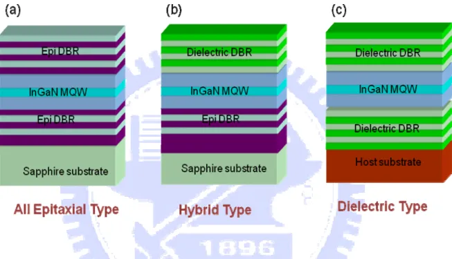
In recent years, several efforts have been devoted to the realization of nitride-based VCSELs [18-27]. Currently, three kinds of structures were reported:
I. Fully epitaxial grown VCSEL structure
In 2005, J. F. Carlin [27] and E. Feltin [28] demonstrated the wholly epitaxial and
high quality nitride-based micro-cavity (as shown in figure 1.4(a)) using metalorganic vapor phase epitaxy (MOVPE or MOCVD). They used the lattice-matched AlInN/GaN as the bottom and top reflectors to avoid cracks happened due to the accumulation of the strain after stacking large pairs of layers. The reflectivity of AlInN/GaN could be achieved as high as 99.4%. They showed the 3/2-lambda cavity emitted a very narrow emission with a linewidth of 0.52 nm, corresponding to a quality factor of ~800.
II. VCSEL structure with two dielectric mirrors
Compared to epitaxial grown reflectors, the fabrication of dielectric mirrors is relatively simple. Furthermore, the large index difference of dielectric mirrors makes them could easily have wide stop band (>50nm) and high reflectivity (>99%) by coating just few stacks of 1/4-lambda-thick layers. Therefore, using dielectric mirrors to accomplish nitride-based VCSELs had begun attractive. Song et al. [19],
Tawara et al. [20] and J. T. Chu et. al. [22] successively reported the structure (as
shown infigure 1.4(c)) after 2000. They employed some process techniques such as wafer bonding and laser lift-off to make dielectric mirrors be coated onto both sides of nitride-based cavity. They showed a micro-cavity could have a very high quality factor to be greater than 400 and achieve lasing action using optical pumping. In addition , Takashi Mukai et al [23] have demonstrated the CW lasing at room
temperature in a GaN-based vertical-cavity surface-emitting laser (VCSEL) by current injection in 2008. Its optical cavity consisted of a 7λ-thick GaN semiconductor layer and an indium tin oxide layer for p-contact embedded between two SiO2/Nb2O5 dielectric distributed Bragg reflectors. The threshold current of
VCSEL is 13.9kA/cm2 and the lasing wavelength is about 414nm. However, the
fabrication techniques of this kind of VCSEL is relatively complicated, and its cavity length can not be efficiently controlled due to polishing problems.
III. VCSEL structure with hybrid mirrors
The so-called hybrid mirrors are a combination of two different kinds of reflectors, for example, a dielectric mirror and an epitaxial reflector. Typically, the fabrication of this structure is to grow bottom reflector and cavity using MOCVD
and then coat dielectric mirror to complete VCSEL structure (as shown in figure 1.4(b)). The hybrid-cavity nitride-based VCSEL\formed by the dielectric mirror and the epitaxially grown high-reflectivity GaN/AlxGa1-xN DBR was reported earlier. In
1999, Someya et al. [18] used 43 pairs of Al
0.34Ga0.66N/GaN as the bottom DBR and
reported the lasing action at ~400nm. Then, Zhou et al [21] also employed a bottom
DBR of 60 pairs Al0.25Ga0.75N/GaN and observed the lasing action at 383.2nm. Both
these AlGaN/GaN DBR structures required large numbers of pairs due to the relatively low refractive index contrast between AlxGa1-xN and GaN. Therefore, recently some groups began to study the AlN/GaN for application in nitride VCSEL. The DBR structure using AlN/GaN has higher refractive index contrast (Δn/n=0.16)[29] that can achieve high reflectivity with relatively less numbers of
pairs. It has wide stop band that can easily align with the active layer emission peak to achieve lasing action. However, the AlN/GaN combination also has relatively large lattice mismatch (~2.4%) and the difference in thermal expansion coefficients between GaN (5.59x10⁻⁶/K) and AlN (4.2x10⁻⁶/K) that tends to cause cracks in the
epitaxial film during the growth of the AlN/GaN DBR structure and could result in the reduction of reflectivity and increase in scattering loss. With the mature of epitaxy techniques, the high-reflectivity AlN/GaN DBR structure with relatively
smooth surface morphology has become possible with just twenty or thirty pairs [30].
In comparison of these three VCSELs, it doesn’t require complicated process such as laser lift-off technique to complete a hybrid VCSEL device. This means the fabrication of such structure is stable and reliable comparing to other structures. Thus, the hybrid structure is more advantageous in the aspects of fabrication and commercialization In fact, the investigation of the characteristics of the GaN-based VCSELs has gradually attracted more attentions. Kako et al. [31] investigated the
coupling efficiency of spontaneous emission (β) and the polarization property of the nitride VCSEL and obtained a high β value of 1.6×10⁻² and a strong linear
polarization of 98%. Tawara et al. [20] also found a high β value of 10-2 in the nitride
VCSEL with two dielectric mirrors. Honda et al. reported the estimation of high characteristics temperature of GaN-based VCSEL [32]. These all mean the
development of nitride-based VCSEL and the understanding of the laser performance has become more and more important.
1.3 The main challenges for electrically pumped GaN-based VCSELs
The difficulty in the realization of an electrically pumped GaN-based VCSEL mainly comes from two factors. First is the requirement of high reflectivity and high quality distributed Bragg reflectors (DBRs). The reported DBR structure that is composed of AlxGa1−xN and GaN , which has the small refractive index
contrast(~6%) . 50 pairs AlxGa1−xN/GaN DBR were need to reach reflectivity of 99%
in the stop band. The large number of DBR easily cause the production of cracks within the GaN cavity. These cracks in the DBR could result in the reduction in optical reflectivity and increase in the scattering loss. Moreover, the cracks could also become a current leakage path, making the realization of an effective current injection into GaN VCSEL very difficult. The AlN/GaN DBR have larger index difference (~20%) and small number of DBR pairs to reach high reflectivity , but lager lattice mismatch than AlGaN/GaN DBR. Many research groups have studied and reported the approaches of using GaN/AlGaN or AlN/AlGaN superlattice (SL) insertion layers to reduce the biaxial tensile strain and successfully suppress crack generation while growing high Al-contained structures. Our group have reported the growth of the crack-free 20-pair GaN/AlN DBRs with insertion of three sets of 5.5 periods of GaN/AlN SL during the growth and the achievement of high reflectivity with wide
stop-band width[33]. We apply this technique to fabricate the crack-free, high
reflectivity AlN/GaN DBR for the hybrid DBR VCSEL.
The second factor is the need for a high transparency yet good conductivity contact for injection of the carriers into the multiple quantum well (MQW) active region. Since the p doping of GaN is very difficult, the carrier injection path with low resistance and optical loss is required for efficient current injection. For this issue , we deposit an ITO layer above the p-type GaN as an transparency conductive layer. Current can spread uniformly by mean of ITO layer before entering the p-type GaN. This transparency conductive layer can efficiently reduced the series resistance of electrically driven devices.
1.4 Outline of the thesis
This thesis is organized in the following manner. In chapter 2 , we first introduce the previous work of our group and simulate the reflectance spectra of different ITO thickness. The lasing characteristics of optical pumped VCSELs are showed in chapter 3. As shown in chapter 4, we observed the characteristics of four different ITO thin film. In chapter 5, we present the optical and electrical performance of electrically driven VCSELs with four different ITO layer. Finally, chapter 6 are the conclusion and future work.
Chapter 2
Motivation
2.1 Previous work of our group
2.1.1Optical pumped VCSEL[33]
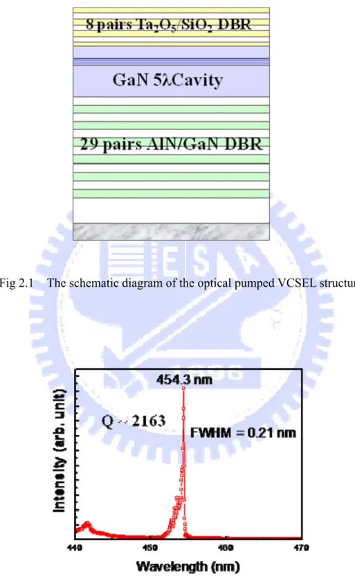
In our previous work, the characteristics of an optical pumped GaN-based VCSEL was successfully fabricated and investigated. The schematic diagram of the overall VCSEL structure are shown in the Fig 2.1 . The hybrid DBR VCSELs structure is composed of 2-inch diameter c-plane sapphire , 2um thickness GaN buffer layer , 29 pairs AlN/GaN DBR , 5λ GaN cavity and 8 pairs Ta2O5/SiO2 upper DBR. The
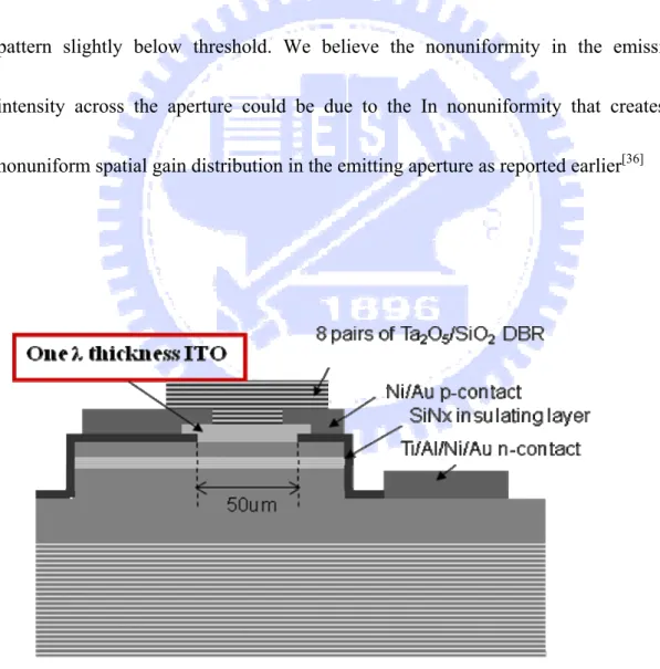
reflectivity of lower and upper DBR are all about 99%. A narrow PL emission with full width at half maximum of 0.21nm corresponds to the cavity resonant mode at 454.3nm was observed, as shown in Figure 2.2. The cavity quality factor, estimated from the emission linewidth of 0.21nm, was about 2200. Figure 2.3 shows the laser action was achieved under the optical pumping at room temperature with a threshold pumping energy (Eth) of about 55 nJ corresponding to an energy density of 7.8
mJ/cm2. A dominant laser emission line at 448.9 nm appearing above the threshold
Fig 2.1 The schematic diagram of the optical pumped VCSEL structure
Fig 2.3 The excitation energy - emission intensity curve (L-I)
2.1.2 CW lasing of current injected GaN-based VCSEL at 77k
[34]With the achievement of optically pumped GaN-based VCSEL, the realization of electrically-injected GaN-based VCSEL has become promising. Fig 2.5 is the overall current injected VCSEL structure. The resonant cavity structure has an 0ne optical wavelength thickness ITO layer deposited on the p-type GaN layer compared with optical pumped cavity. The ITO layer can be used as a transparent conduct layer(TCL) and improve the current spreading problem resulting from low conductivity of p-GaN. In addition ,One optical wavelength thickness can match the resonance phase condition of microcavity and reach high transmittance(~98%) for ITO layer. However , we can find that the quality factor of electrically pumped cavity is about 900 from PL spectrum , as shown in Fig 2.6. The value of quality factor is about half of the optical pumped result due to additional ITO absorption. We consider the loss of ITO maybe one of the main challenges for us to reach CW lasing in current injected VCSELs at room temperature.
In order to observe the lasing behavior in current injected VCSEL, we packaged our devices into TO can. The packaged VCSEL device was mounted inside a cryogenic chamber for testing under cw current injection condition using a cw current source at 77 K. Fig2.7 shows the light output power versus cw injection current
output power showed a distinct threshold characteristic at the threshold current (Ith) of about 1.4 mA and then was linearly increased with the injection current beyond the threshold. The threshold current density is estimated to be about 1.8 kA/cm2 for a
current injection aperture of 10 um in diameter, assuming the current is uniformly injected within the aperture. The lasing wavelength is 462.8nm with 0.15nm line width shown in Fig2.8. The inset of Fig3.8 is the CCD image of the spatial l emission pattern slightly below threshold. We believe the nonuniformity in the emission intensity across the aperture could be due to the In nonuniformity that creates a nonuniform spatial gain distribution in the emitting aperture as reported earlier[36]
Fig2.6 emission spectrum of the current injected VCSEL structure.
Fig 2.8 The laser emission spectrum at different injection current levels measured at 77 K.
2.2 Reflectance spectra simulation
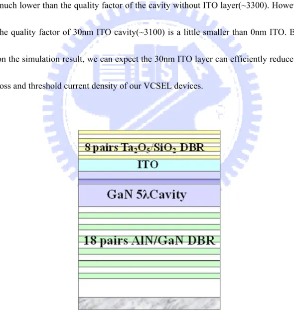
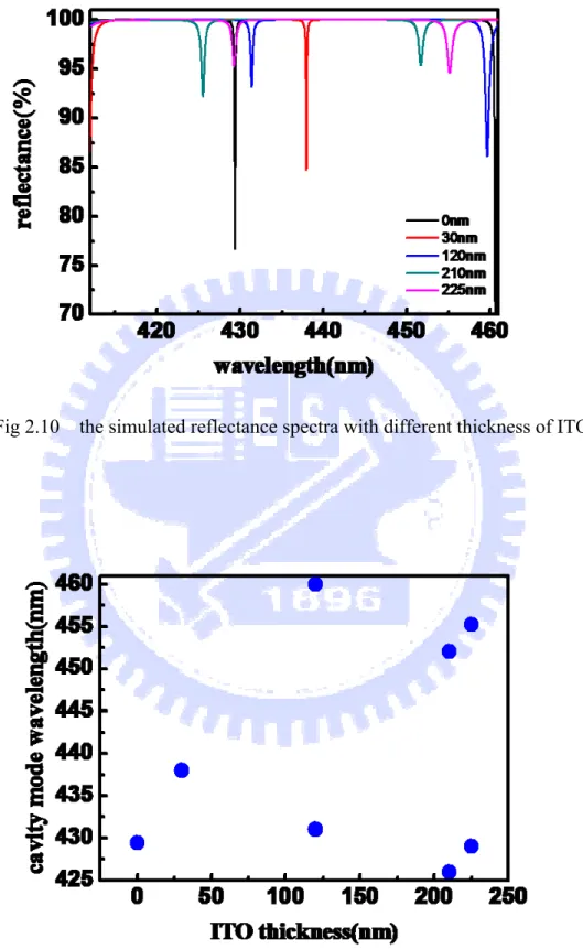
So far, our group have fabricated and demonstrated the cw operation of an electrically pumped GaN-based VCSEL at 77 K. Next step, we should work toward the cw lasing of current injected devices at room temperature. In order to reach the goal, we should try to reduce the loss of ITO so that the threshold current can also be lower at room temperature. In general, the thinner layer has the smaller absorption for the same material, so we would like to replace previous 0ne optical wavelength thickness ITO with thinner ITO layer. Before proceeding with the experiment , we first simulate the reflectance spectra with different thickness of ITO layer. Fig2.9 shows the cavity structure of simulation, and ITO layer thickness are 0nm、30nm、 120nm、210nm and 225nm (about one optical wavelength thickness for 440nm). Owing to reflectivity symmetry of DBR , the AlN/GaN DBR are chosen to 18 pairs. Fig 2.10 are the simulated reflectance spectra of different ITO thickness. The dip positions in the reflectance spectra represent the cavity mode of these cavities , and the quality factor can be estimated form the linewidth of the dip. Fig 2.11 shows the cavity mode wavelength versus different ITO thickness. The cavity mode wavelength shift to longer wavelength because of the increase of the cavity length, but the cavity mode wavelength return to shorter wavelength when the ITO thickness is thicker than
120nm. This phenomenon is due to the exceeding the stop band region of the lower DBR , so that the cavity mode jumps to the (m+1)th mode from the mth mode.
Furthermore, the cavity mode also change to multimode owing to longer cavity length and smaller mode spacing , when ITO thickness is lager than 30nm. In Fig2.12 , we can observe that the quality factor is about 700 in 225nm ITO cavity , but this value is much lower than the quality factor of the cavity without ITO layer(~3300). However, the quality factor of 30nm ITO cavity(~3100) is a little smaller than 0nm ITO. Base on the simulation result, we can expect the 30nm ITO layer can efficiently reduce the loss and threshold current density of our VCSEL devices.
Fig 2.10 the simulated reflectance spectra with different thickness of ITO
Chapter 3
Characteristics of an Optical Pumped GaN-Based VCSEL
3.1 optical measurement system
Figure 3.1 shows the optical pumping scheme for our VCSELs. As shown in Fig. 3.1 the emission spectrum of the GaN-based VCSEL structure was measured using a microscopy system (WITec, alpha snom) at room temperature. The optical pumping of the samples was performed using a frequency-tripled Nd:YVO4 355-nm pulsed laser with a pulse width of 0:5 ns at a repetition rate of 1 kHz and a He-Cd 325nm cw laser. The pumping laser beam with an about 50um spot size was incident normal to the VCSEL sample surface. The light emission from the VCSEL sample was collected using an imaging optic into a spectrometer/charged coupled device (Jobin-Yvon Triax 320 Spectrometer) with a spectral resolution of 0:1 nm for spectral output measurement.
3-2 Fabrication and characteristics of optical pumped VCSELs
The overall optical pumped GaN VCSEL structure is shown in Fig 3.2. The mirocavity and bottom DBR structure are grown in a vertical-type MOCVD system (EMCORE D75), which can hold one 2-inch sapphire wafer. The nitride-based DBR used in the experiment is the stacks of 29-pair AlN/GaN layers with insertion of the AlN/GaN super-lattice (SL). The super-lattice in structure is inserted for releasing strain during the growth of AlN/GaN DBR to further improve interface and raise reflectivity of the DBR. Fig3.3 is the reflectance spectrum of bottom DBR, and there is a high reflectivity (~99.3%) at 440nm. The stop band of bottom DBR is as wide as about 20nm.
Then, a micro-cavity formed by a p-n junction was grown following the growth of the DBR structure. The micro-cavity composed of about 860-nm-thick n-type GaN, a ten pairs In0.2Ga0.8N/GaN (2.5 nm/7.5 nm) MQW, 24nm AlGaN electron blocking
layer, a 115-nm-thick p-type GaN and 2nm InGaN layer. The cavity length is about 7-λ in optical length. The 2nm InGaN layer is used for reduction the Schottky barrier height between ITO and p type GaN layer[37], and it can also improve current
spreading when current inject. The SEM cross-section image is shown in Fig3.4 , and Fig3.5 are the PL spectrum and reflectance spectrum of VCSEL sample without upper
DBR. Obviously, the cavity mode is at about 435nm.
The final process to complete a VCSEL is the deposition of a dielectric mirror. The dielectric mirror in the experiment, an eight pairs Ta2O5/SiO2 DBR, was deposited
using the electron beam evaporation. The dielectric mirror was coated onto as-grown sample surface in an O2 ambient at the controlled temperature about 150℃. The reflectivity spectrum of the dielectric mirror was measured as shown in Fig 3.6 The Ta2O5/SiO2 DBR shows a very high reflectivity as high as 99% centered at 450 nm
with a wide stop-band of about 100 nm.
Fig3.7 is the PL spectrum of GaN-based VCSEL with bottom and upper DBR. The cavity mode wavelength is about 440nm with a 0.24nm linewidth , and the quality factor estimated from PL spectrum is as high as 1900. The lasing behavior can be observed under optical pumping at room temperature in Fig3.8 . The threshold pumping energy density is about 3.3mJ/cm2, and this lower value compared with the
previous result of our group represents the improvement of epitaxial quality, so that the internal loss and threshold energy density is reduced. Fig3.9 shows the lasing spectrum above the threshold condition, and the lasing wavelength is 438nm with a 0.15nm linewidth.
Fig 3.2 The schematic diagram of the optical pumped VCSEL structure
Fig 3.3 The reflectance spectrum of bottom DBR
380 400 420 440 460 480 500 0 20 40 60 80 100
Ref
lectance(
%
)
Wavelength(nm)
R ~99.3%Fig 3.4 The cross section SEM image of VCSEL cavity without upper DBR
Fig 3.5 the PL and reflectance spectrum of VCSEL without upper DBR
380 400 420 440 460 480 500 -0.5 0.0 0.5 1.0 1.5 2.0 2.5 3.0 3.5 4.0 re flect a nc e(% ) wavelength(nm) intensity(a.u) 0 20 40 60 80 100
Fig 3.6 The reflectance spectrum of upper DBR 430 435 440 445 450 0 1 2 3 4
Intensity(arb. unit)
Wavelength(nm)
439.9nm 0.23nm350
400
450
500
550
600
0
10
20
30
40
50
60
70
80
90
100
R
eflectance(
%)
wavelength(nm)
R~99%Fig 3.8 The pumping energy density versus normalized intensity diagram 0.0 0.5 1.0 1.5 2.0 2.5 3.0 3.5 4.0 4.5 5.0 5.5 0 2 4 6 8
Normaliz
ed intensity(a.u)
Pumping energy density (mJ/cm
2)
Threshold energy density~3.3mJ/cm2
430 435 440 445 450 1 2 3 4 5 6 7
Intens
ity(ar
b. unit)
Wavelength(nm)
438.4nm FWHM~0.15nmChapter 4
Characteristics and measurement of indium-tin-oxide
4.1 Introduction to indium-tin-oxide
4.1.1 Transparent conduct layer (TCL)
Gallium nitride (GaN) is an attractive material which has a wide direct band gap, GaN-based optoelectronic devices such as light emitting diodes (LEDs) and laser diodes (LDs) have been researched and commercially available . Most commercial GaN-based devices use an Mg-doped GaN layer as a p-type semiconductor . However, the high activation energy (~180 meV) of Mg atoms leads to only 1% of Mg atoms can be ionized, and therefore the carrier concentration of p-type GaN is quite low and the poor conductivity will limit current spreading laterally. It is necessary to deposit a conductive layer on p-GaN for current spreading. This layer should not only form good ohmic contacts to p-GaN but also be transparent to the emitted light from the active layer.
Because of the high work function of p-GaN , metal of higher work function such as Ni , Pd and Pt were used to form ohmic contact for p-GaN. In gereral, Ni/Au contact is widely applied in commercially GaN-based LED. The specific contact
resistance can reach 10-2~10-6 Ω·cm2 after annealing. However , the Ni/Au layer is a semitransparency layer , and it has been reported that the transmittance of Ni/Au is only around 60% to 85% in the 450-550 nm wavelength [38]. The absorption of contact
layer is important issue for semiconductor laser , because the optical absorption would raise the threshold gain for laser emission. To improve the transmittance of current spreading layer, it is feasible to replace the conventional Ni/Au contact by a better transparent conductive contact. Nowadays , the ITO film has been widely used as a transparent conductor due to its high transparency (~90%) in the visible spectrum and its low electrical resistivity (< 103Ω·cm).
4.1.2 Characteristics of ITO
Indium tin oxide (ITO) thin film have been studied extensively for optoelectronic device application owing to its unique transparency and conduction properties . It is a mixture of indium (III) oxide (In
2O3) and tin (IV) oxide (SnO2)(typically 90% In2O3,
10% SnO
2 by weight) and highly degenerate n-type semiconductor , which has a wide
band gap (~3.5–4.3 eV) and low electrical resistivity (2~4×10⁻⁴Ωcm). The oxygen vacancies accompanied with the Sn donor , which are responsible for high conductivity, can also lead to non-stoichiometric ITO. The optical characteristics of
ITO shows high absorption in UV region , high transmittance in visible region and high reflectance in IR region. In addition, ITO thin film is thermal stable and has better device reliability compared with Au-based contact. Due to these unique properties, ITO has been used in a wide range application, such as transparent electrode for display and solar cell , IR reflective mirror for building and transparent conduct layer for nitride-base devices.
There are many method to deposit ITO thin film including sputtering , e-gun evaporation , chemical vapor deposition , pulsed laser deposition and sol-gel process. In this study , we use e-gun evaporation and sputter deposition to deposit four different structure ITO layer(e-gun 210nm and 30nm amorphous ITO , sputter 30nm crystalline ITO and sputter 10nm amorphous + 20nm crystalline ITO ).
4.2 Measurement method and equipments
4.2.1 Scanning electron microscopy (SEM)
Scanning electron microscope (SEM) is a type of electron microscope that images the sample surface by scanning it with a high-energy beam of electrons in a raster scan pattern. The electrons interact with the atoms that make up the sample producing signals that contain information about the sample's surface topography, composition and other properties such as electrical conductivity. The signals result from interactions of the electron beam with atoms at or near the surface of the sample. In the most common or standard detection mode, secondary electron imaging or SEI, the SEM can produce very high-resolution images of a sample surface, revealing details about 1 to 5 nm in size. Due to the way these images are created, SEM micrographs have a very large depth of field yielding a characteristic three-dimensional appearance useful for understanding the surface structure of a sample. Fig 4.1 is the SEM equipment of our group.
4.2.2 Four point probe
The 4-point probe setup consists of four equally spaced tungsten metal tips with finite radius. Each tip is supported by springs on the other end to minimize sample damage during probing. The four metal tips are part of an auto-mechanical stage which travels up and down during measurements. A high impedance current source is used to supply current through the outer two probes; a voltmeter measures the voltage across the inner two probes (See Fig4.2) to determine the sample resistivity. Typical probe spacing s ~ 1 mm. Fig 4.3 is the four point probe we used to sheet resistance measurement in NCTU NFC.
Fig 4.3 four point probe in NCTU Nano Facility Center
4.2.3 Circular Transmission Line Model (CTLM) measurement
In order to realize the interfacial characteristics between ITO and p type GaN, we make use of CTLM (Circular Transmission Line Model) to measure the specific contact resistance. First, we clean the LED sample and deposit the ITO thin film on p-GaN surface. Then , we etch the ITO to form CTLM pattern after Photolithography Process. Fig 4.4 is the CTLM pattern after ITO etching and removing the photo resist. The CTLM pattern is a series of ring with the identical inner circle and different gap distance. The gap region is only p-GaN surface and the other is all ITO layer. By
and plot RT. versus gap distance, as shown in Fig5.5. If the voltage is impressed two
of these contacts , separated by d , then the equation of total resistance can be derived as follow:
2
(
2
T)
S Td
L
R
R
=
+
π
ρ
(5.1)Where ρs is the sheet resistance of semiconductor material between the contacts . LT
is the transfer length that donates the 1/e distance , which the voltage curve decay nearly exponentially with distance . After fitting the linear curve of the Fig 5.5, we can get the value of ρs and LT . Finally , take these value into the equation 5.2 , and
then we calculate the specific contact resistance( ρc ) of between ITO and p-GaN
layer.
ρ
C=
ρ
S×
(
L
T)
2 (5.2)The potential distribution under the contact can be determine by both ρs and ρc
according equation 5.3.
sinh(
/
)
]
/
cosh[
)
(
T C T C SL
L
W
L
x
L
I
x
V
=
ρ
ρ
−
(5.3)Where L is the contact length , WC the contact width , and I the current flowing into
the contact.
Fig 4.5 the schematic diagram of total resistance versus gap distance
4.3 Result and discussion
4.3.1 Specific contact resistance
In this thesis , we use four different ITO structure deposited by E-gun evaporation and sputter. The annealing parameter for sputter ITO have not yet be realized for our group , so we utilized the CTLM to measure specific contact resistance of different annealing condition. Deposited ITO thin films were annealed using a rapid thermal annealing (RTA) system in nitrogen atmosphere. The annealing temperature and time
shown in Fig4.6(a) and Fig4.6(b) . Fig4.6(a) demonstrates the specific contact resistance at fixed annealing temperature (600℃) , and Fig4.6(b) was measured for the same annealing time (10mins). As shown in these two figures , we can find that there is a minimum specific contact resistance(~0.2Ωcm2) at 600℃ with annealing time of 10mins , so we applied this parameter for ITO annealing before other measurement.
Fig 4.6 ITO specific contact resistance (a)with different annealing time and(b) with different annealing temperature
4.3.1 ITO surface morphology
In this section , we use scanning electron microscopy(SEM) to observe the surface morphology of ITO thin film. The top-view SEM image are shown from Fig 4.7(a) to Fig 4.7(d). Fig4.7(a) and Fig4.7(b) are the 30nm ITO layer deposited by sputter. The difference of them is that the former is deposited at 150℃ , and the latter is
continue residual layer. While depositing at 150℃ , ITO thin film can be crystalline compared with at room temperature. Despite the slight difference in deposition temperature , the surface morphology of them are similar , and the grain size is as small as below 10nm diameter. As shown in Fig4.7(c) and Fig4.7(d) , the 30nm and 210nm ITO deposited by E-gun have lager grain size(~30nm in Fig4.7(c)) and amorphous structure.
Fig 4.7 (a) sputter 150℃ crystalline 30nm ITO (b) sputter 10nm amorphous + 20nm crystalline ITO
4.3.3 Refractive index and extinction coefficient
To realize the material absorption characteristics of ITO , we measure the refractive index and extinction coefficient by mean of n&k analyzer 1280. The schematic diagrams of wavelength dependence of refractive index and extinction coefficient for four different ITO layer are shown from Fig 4.8 (a) to Fig 4.8 (d). Fig 4.8(a) and Fig 4.8(b) are the measurement result of sputter 30nm crystalline ITO and sputter 10nm α+ 20nm crystalline ITO. The curves of experimental data are nearly identical , and this appearance may be due to the same deposition source and thickness. The extinction coefficient has a maximum in ultraviolet region , it means the high absorption because of interband transition or atomic oscillation[39]. In visible region,
the extinction coefficient is nearly zero . It represents the most of light is transparent and this material is almost colorless. The value of absorption in transparent region gradually increases as wavelength approach infrared region. This increase is owing to the vibrational absorption associated with lattice vibration. As shown in Fig 4.8 (c), the extinction coefficient of 30nm deposited by E-gun is especially lower than other three kind of ITO layers , and absorption curve does not raise near IR region. We suppose this phenomenon is due to larger spacing between lager grain size , so this ITO thin film has lowest absorption but current would spread more difficultly. Fig
4.8(d) shows the higher absorption in longer wavelength than others during visible region . That is why the one optical wavelength thickness usually exhibit green appearance.
Fig 4.8 the refractive index and extinction coefficient versus wavelength diagram for sputter (a) 30nm crystalline ITO (b) 10nm α+ 20nm crystalline ITO
200 400 600 800 1000 1.8 1.9 2.0 2.1 2.2 2.3 2.4 n k
Ext
inction co
ef
ficient
Re
fra
ti
v
e index
wavelength(nm)
0.0 0.1 0.2 0.3 0.4 0.5 200 400 600 800 1000 1.8 1.9 2.0 2.1 2.2 2.3 2.4 n kExt
inction co
ef
ficient
Re
fra
ti
v
e index
wavelength(nm)
0.0 0.1 0.2 0.3 0.4 0.5Fig 4.8 the refractive index and extinction coefficient versus wavelength diagram for E-gun (c) 30nm ITO (d) 210nm ITO
200 400 600 800 1000 1.8 1.9 2.0 2.1 2.2 n k
Ext
inction co
ef
ficient
Re
fra
ti
v
e index
wavelength(nm)
0.0 0.1 0.2 0.3 0.4 0.5 200 400 600 800 1000 1.5 1.6 1.7 1.8 1.9 2.0 2.1 2.2 2.3 n kExt
inction co
ef
ficient
Re
fra
ti
v
e index
wavelength(nm)
0.0 0.1 0.2 0.3 0.4 0.54.3.4 Summary
Table4.1 is the summary of ITO characteristics. The 30nm ITO thin film show the larger sheet resistance and resistivity than 210nm ITO layer. The sheet resistance is associated with lateral current spreading , and it generally decreases as thin film thickness increase. The value of resistivity is affected by defects density within thin film layer. Due to thinner deposition thickness, 30nm ITO has still more defects than 210nm ITO. These defects would cause electron scattering and reduction of Hall mobility[40]. However , the specific contact resistance between ITO and p-GaN of
30nm ITO are slightly lower than 210nm ITO layer. This result reveals the specific contact resistance is related to annealing parameter , not thin film thickness. Especially , the 30 nm ITO layer deposited by E-gun has the largest sheet resistance and resistivity but the lowest absorption among four different structure ITO layer. We suppose that it may be resulted from more defect of vacancies . The deposition quality of E-gun evaporation should be promoted when deposition thickness is too thin.
Chapter 5
Fabrication and measurement of electrically driven
GaN-based VCSELs
5.1 GaN-based VCSELs process
5.1.1 Initial clean and photolithography technique
During process of GaN-based VCSELs, two basic skills will be frequently used. One is the initial clean (I.C.), and another is photolithography technique. The purpose of the I.C. is to remove the small particle, and organism on the sample surface, before we start any process procedure. The steps of I.C. are described as below :
1. Degreasing by ultrasonic baths in acetone (ACE) 5min.
2. Dipping by ultrasonic baths in isopropyl alcohol (IPA) 5min for organism removed. 3. Rinsing in de-ionized water (D.I. water) 5min for surface clean.
4. Blowing with N
2 gas for surface drying.
5. Baking by hot plate 120oC, 5min, for wafer drying.
The purpose of the photolithography is to transfer the pattern of the mask to the photoresist (PR) on the wafer. In the process of photolithography, a positive
photoresist AZ 5214E was used. Although it is positive photoresist , it is capable of image reversal (IR) resulting in the effect of negative photoresist. In fact AZ 5214E is almost exclusively used in the IR-mode which is proper to be used in the lift-off process. Both positive exposure and IR exposure photolithography technique were employed in our VCSEL process. These photolithography techniques are described as below:
Positive exposure technique
1.Spin coating by photoresist (1000rpm/10s, 3500rpm/30s). 2. Soft bake: hot plate 90oC, 90sec.
3. Alignment and exposure
4. Development: dipping in AZ-300 for 30sec. 5. check exposure PR pattern by OM.
6. Hard bake: hot plate 120oC, 4min
IR exposure technique
1.Spin coating by photoresist (1000rpm/10s, 3500rpm/30s). 2. Soft bake: hot plate 90oC, 90sec.
4.Hard bake 120℃ 110sec 5.Exposure without mask 57sec
6. Development: dipping in AZ-300 for 30sec. 7. check exposure PR pattern by OM.
8. Hard bake: hot plate 120oC, 4min
6.1.2 Process flowchart
The sample structure we use in our process is the same as Fig3.2 without depositing upper DBR. To fabricate the VCSELs device on chip , we need to experience six process steps. Fig 5.1 is the schematic diagram of overall VCSELs process flowchart. In the beginning , SiNx mesa etching mask and ICP dry etching machine were used to define the mesa region . As shown in Fig 5.2 , we check the electrically properties by probe station after mesa was finished. Then, 200nm SiNx layer was deposited by PECVD and patterned to form current confinement layer with effective current aperture varying from 15um to 40um. The four different structure ITO , which was mentioned earlier , were deposited individually by E-gun or sputter , and annealed at RTA system under nitrogen ambient. The ITO transparent conduct layer on a 40um current aperture after etching is shown in Fig 5.3. The Ti/Al/Ni/Au and Ni/Au
contacts was deposited to serve as n-type and p-type electrode, respectively.The final step is deposition of 10pairs SiO2/Ta2O5 dielectric DBR as upper mirror. The
schematic diagram of completed electrical pumped VCSEL is shown in Fig 5.4 , and Fig5.5 is the OM image of VCSEL device with 5um metal aperture when current injects.
Fig 5.2 The defined mesa of first step was measured by probe station
Fig 5.4 The schematic diagram of completed electrical pumped VCSEL
5.2 The electroluminescence (EL) measurement system
The electroluminescence (EL) characteristics of fabricated VCSELs were measured by the probe station system and evaluated by injecting different current density. The device is driven by Keithley 238 CW current source, and its light output power could be measured by optical power meter through a integrated sphere. Current-light output power (L-I) and current-voltage (I-V) measurements were performed by using the probe station, Keithley 238 CW Current Source, UV power detector, Newport 1835-C optical power meter. Figure 5.6 shows the electrical and optical measurement system. The emission signal could be received by CCD and observed on the CRT screen. The direct emission from device is collected by 40X microscope and transmitted to Jobin-Yvon Triax 320 spectrometer by optical fiber with 25μm in diameter. All the data could be directly fee-backed to the computer from these facilities, including optical meter spectrometer and Keithley 238 current source by the GPIB connector.
5.3 The characteristics of GaN-based VCSEL at Room temperature
In this thesis , we applied four different ITO thin film on our VCSEL devices , so we would introduce the optical and electrical characteristics of them , respectively.
5.3.1 VCSEL devices with 210nm ITO deposited by E-gun evaporation
The 210nm ITO layer , which has nearly one optical wavelength thickness , deposited on our VCSEL device is used as an reference compared with the devices with 30nm ITO thin film. Fig5.8(a) is the power and voltage versus current density diagram (LIV curve) . The series resistance and turn on voltage of devices are about 202Ω and 6.5V, respectively. The output power begin to roll over when current density reaches 11kA/cm2 . These electrically characteristics are better than the result
we reported earlier [34] , as shown in Fig 5.7. This improvement of electrically
performance reveals the promotion of our epitaxial quality in these years. We also observed the optical intensity distribution by mean of CCD and Beam-view program . The color on Fig 5.8(b) represents the relative optical intensity emitted from the observed device , and this figure shows the percent of optical intensity within the aperture region(circle of dotted line) is 53% . It means about 50% of emission escapes
from the edge of mesa due to poor lateral optical confinement in our devices. The reduction of emission from the aperture would promote the threshold condition for lasing. Fig 5.9 is the electroluminescence spectrum of VCSEL device with 30um metal aperture and the inset is the CCD image of current aperture. The cavity mode and quality factor estimated from this spectrum are 420nm and about 700, respectively. There are several bright spots within the current aperture , which maybe attributed to the inhomogengity of nitride DBR. These bright spots represent the high quality region on the sample surface , so we suppose the spectra of narrow linewidth are received from there .
Fig 5.8 (a) LIV curve and (b) optical intensity distribution of VCSEL with 210nm ITO
Fig 5.9 The EL spectrum of VCSEL device with 210nm ITO, and the inset figure is the CCD image of the current aperture
5.3.2 VCSEL devices with 30nm ITO deposited by E-gun evaporation
The electrically characteristics of VCSEL with 30nm ITO deposited by E-gun are shown in Fig 5.10 (a) and (b). The series resistance and turn on voltage of devices are about 182Ω and 7V, respectively. The output power reaches a maximum when the device is operated at 11.8kA/cm2. These performance can be comparable to the
highest sheet resistance mentioned at earlier chapter. The carriers do not spread uniformly before entering the p-GaN layer , so that the emission area is broader and inhomogeneous near current aperture. More emitted light can escape from cavity through neighbor edge of mesa. Although the worse current spreading observed in VCSEL device with 30nm ITO deposited by E-gun , the quality factor measured from Fig 5.11 is about two time lager than 210nm ITO . The improvement of quality is due to the lower optical absorption of thinner ITO layer , and it can confirm our expectation of using 30nm ITO to replace thicker ITO layer.
Fig 5.10 (a) LIV curve and (b) optical intensity distribution of VCSEL with 30nm ITO deposited by E-gun
Fig 5.11 The EL spectrum of VCSEL device with 30nm ITO deposited by E-gun , and the inset figure is the CCD image of the current aperture
5.3.3 VCSEL devices with 30nm crystalline ITO deposited by sputter
The electrically characteristics of VCSEL with crystalline 30nm ITO deposited by sputter are shown inFig 5.12 (a) and (b). The series resistance and turn on voltage of devices are about 164Ω and 5V, respectively. The roll over current density of devices is 13 kA/cm2 , and the percent of optical intensity within the current aperture
is 37% , slightly higher than E-gun 30nm ITO layer. The electrically characteristics of sputter ITO is better than which deposited by E-gun for the same thickness , but the total loss within resonant cavity obtained indirectly from quality factor showed in Fig 5.13 is similar . The equation , which associates the quality factor and total loss, is as follow: (5.1)
λδ
π
λ
λ
nL
Q
=
2
Δ
=
Fig 5.12 (a) LIV curve and (b) optical intensity distribution of VCSEL with crystalline 30nm ITO deposited by sputter
Fig 5.13 The EL spectrum of VCSEL device with crystalline 30nm ITO deposited by sputter, and the inset figure is the CCD image of the current aperture
5.3.4 VCSEL devices with 10nmα+20nm crystalline ITO deposited by sputter The electrically characteristics of VCSEL with 10nmα+20nm crystalline ITO deposited by sputter are shown in Fig 5.14 (a) and (b). The series resistance and turn on voltage of devices are about 165Ω and 5V, respectively. The roll over current density of devices is 14 kA/cm2 . The cavity mode and quality factor estimated from
the spectrum showed in Fig 5.15 are 415.2nm and about 1600, respectively. These electrical and optical performance are comparable to the ITO thin film deposited by the same source. However , the percent of optical intensity within current aperture is as high as 94% , and this value is the largest compared with other three kinds of ITO thin film. The reason of this unique phenomenon is under investigation. We suppose that it is possible owing to the heterojunction between amorphous and crystalline ITO layer. But , most importantly , the characteristics of this kind of ITO thin film match our demand for GaN-based VCSEL very well.
Fig 5.14 (a) LIV curve and (b) optical intensity distribution of VCSEL with 10nmα+20nm crystalline ITO deposited by sputter