利用脈衝雷射分子束磊晶之氧化鋅薄膜的成長與光學特性研究
54
0
0
全文
(2) semiconductors.4). In 1997, YF Chen et al. 5) evidenced the lasing from ZnO epilayers. grown by MBE with the threshold intensity of 240KW/cm2 . In 1998, Kawasaki et al.,6) found laser operation of ZnO thin film at room temperature grown using Laser-Molecular beam epaxity. The facets of the hexagons observed at the surface of the films contribute to the low threshold of lasing (It=40KW/cm2 ).. The lasing. mechanism is attributed to the exciton-exciton collision process. In order to obtain good quality of ZnO thin film, several growth technologies have been used such as molecular-beam epitaxy (MBE),7) metal-organic chemical vapor deposition (MOCVD),8) pulse- laser deposition (PLD),9) and laser molecular-beam epitaxy (LMBE).10). Among these methods, LMBE has the advantages of ultra-clean,. simplicity, without corrosive gas, and achieving high-quality epitaxial films at a relatively low growth temperature (500℃) due to its high kinetic energy (10eV— 100eV) of laser ablated species. Besides, the source of Zn and O can be obtained directly from the target in LMBE, i.e. no extra oxygen supply is necessary. This process is important for some devices since the oxygen atmosphere during the laser ablation leads to several problems. Firstly, the oxygen will cause the oxidation of the internal parts in the chamber, for example, the substrate holder and other components close to the high temperature-heating lamp. Secondly, the purity of the used oxygen will be changed when it reaches the growth area. Finally, oxygen may result in the degradation of the grown films such as the oxidation of the substrates and oxidation during hetero-epitaxy. Up to now, several reports have discussed the growth conditions to obtain good quality ZnO thin films by using different substrates, oxygen pressures, growth temperatures, and target-to-substrate distances by LMBE. 11). Moreover, the. introduction of thermal annealing under different atmospheres and one additional buffer laye r are also included to greatly improve the quality of ZnO films. -2-. 12,13).
(3) However, fewer studies have been done on the growth of ZnO thin films in vacuum by LMBE.. In this paper, we investigate the growth and the characteristics of ZnO. films grown on c- face sapphire under high vacuum condition (without flowing any oxygen in chamber) by Laser-MBE.. 1.3 Organization of the thesis The thesis consists of five chapters, including the present introduction.. We. introduce the background mechanisms of Laser-MBE as well as the basic theory of some characterization tools of semiconductor such as XRD, photoluminescence (PL) spectroscopies. In chapter 3, we describe the experimental details, including the sample preparation, the equipment setups and parameters of characterization. The results of the ZnO thin film are presented in chapter 4. By means of the XRD, PL, the crystalline changes in the growth conditions have been investigated and discussed. We also described the surface image of the ZnO thin film by AFM. In the final chapter, we conclude our investigations on the ZnO thin films and propose some topics for further study.. -3-.
(4) Fig.1-1. Wurtzite structure,. -4-. : :O,. :Zn. ○.
(5) Chapter 2 Theoretical background. 2.1 The Laser-MBE system and Principle of Laser-MBE deposition 14). 2.1.1. Laser-MBE system layout The system consists [Fig.2-1(a)] of a load lock chamber module and two. deposition chambers. The samples are loaded from the load lock through the UHV gate valves using magnetically coupled transfer arms. Changing the sample from one to another deposition chamber is done by using push-pull- type pick-up manipulator located in the load lock module. The deposition chambers, designed for pulsed laser ablation deposition, are equipped with gas inlet system, target manipulator, substrate manipulator and necessary parts for laser beam inlet, reflection high-energy electron diffraction (RHEED), vacuum monitoring and pumping system. The load lock chamber [Fig.2-1(b)] is a small volume spherical chamber with a Viton sealed quick access door for substrate loading. The substrates are attached on a substrate holder block. The substrate holder block can be moved from the load lock into the deposition chamber by using a magnetically coupled transfer arm. The transfer arm is equipped with adjusting bellows and support rods and a cup-type carrier transferring the sample holder to the substrate manipulator. Fig.2-1(c) shows main chamber with the major components. In addition to the components used directly for the LMBE growth process, the growth chamber may contain various in situ surface analysis equipments to monitor the surface structure and control the growth conditions. This unique feature has played a major. -5-.
(6) role in the understanding of the growth process during the initial development stages of LMBE technology.. The reflection high-energy electron diffraction (RHEED). apparatus is the most useful and important surface analysis instrument in the ordinary MBE growth chamber. It provides a very sensitive information of the outermost layers of atoms of the crystal before and during growth as a function of growth conditions.. It is possible to obtain lots of information concerning substrate. cleanliness, smoothness, and surface structure from the RHEED patterns. Fig. 2-1 shows the geometry of the RHEED apparatus. In the LMBE system, a collimated beam of high energy electrons in the range of 5-40 KeV is directed at a low angle of 1-2o toward the sample surface orthogonal to the molecular beam paths. Because the de Broglie wavelength of an electron at this energy is a fraction of atomic spacing on surface, a diffraction pattern is formed on the fluorescent screen mounted opposite to the electron source.. In this configuration, the sample surface can continuously. monitored without interrupting the growth procedure. Since the component of the incident electron momentum normal to the surface is very small, the penetratio n depth is limited to only the uppermost few atomic layers. On a smooth crystal surface with a lattice constant ao , which acts as a two-dimensional Laue diffraction condition. Using the Ewald construction the reciprocal lattice is composed of rods in reciprocal space in the direction normal to the real surface. At high energies, the de Broglie wavelength ? of the electron is small, and the radius of the Ewald sphere 2p/? is large compared to the typical reciprocal lattices, 2p/ ao . In addition, the reciprocal lattice rods have finite thickness due to lattice imperfections and thermal vibrations, and the Ewald sphere also has finite thickness due to the spread in electron energy and beam convergence. As a result, the intersection of the Ewald sphere and reciprocal lattice rods occurs almost along their length, as incident in Fig. 2-2. This results in a streaked diffraction pattern normal to the shadow edge of the sample. -6-. On the.
(7) contrary, in the presence of microscopic roughness on an otherwise flat surface, the diffraction pattern is formed mainly in transmission through the surface asperities and exhibits a spotty appearance.15) LMBE has the advantages of ultra-clean, simplicity, without corrosive gas, and achieving high-quality epitaxial films at a relatively low growth temperature (500 ℃) due to its high kinetic energy (10eV—100eV) of laser ablated species. Besides, the source of Zn and O can be obtained directly from the target in LMBE, i.e. no extra oxygen supply is necessary.. 2.1.2. Principle of L-MBE deposition To investigate the physics and theoretical nature of the laser-deposition. process, the evaporation of the target material, the formation of a high-temperature plasma by the absorption of laser energy by the evaporated material, and the expansion of the plasma resulting in deposition of thin films is considered in detail. Depending on the type of interaction of the laser beam with the target, the laser deposition process can be classified into three separate regimes: (i) interaction of the laser beam with the target material resulting in evaporation of the surface layers; (ii) interaction of the evaporated material with the incident laser beam resulting in an isothermal plasma formation and expansion, and (iii) anisotropic adiabatic expansion of the plasma leading to the characteristic nature of the laser-deposition process. The first two regimes start with the laser pulse and continue throughout the laser pulse duration. The last regime starts after the laser pulse terminates. Each of the three regimes is considered separately in detail. A. Interaction of laser beam with the target At high power densities obtained from nanosecond excimer- laser pulses,. -7-.
(8) heating and evaporation of the material will occur at the beginning of the laser pulse. The amount of evaporated flux varies linearly with the pulse energy density. B. Interaction of laser beam with evaporated material As the evaporated material is further heated by the interaction of the laser beam, it results in the formation of a high-temperature plasma of ions, atoms, molecules, electrons, etc. The temperature attained by the plasma depends on the power density, frequency, pulse duration of the laser beam, and the optical and thermophysical properties of the material. During the incidence of the laser pulse, the isothermal expanding plasma is constantly augmented at its inner surface with evaporated particle from the target. The acceleration and the expansion velocities in this regime are found to depend upon the initial velocities of the plasma. Because of the large lateral dimensions of the plasma, it expands preferentially normal to the irradiated surface. C. Adiabatic plasma expansion and deposition of thin films After the termination of the laser pulse, this plasma expands adiabatically with the expansion velocities controlled by its initial dimensions. The plasma cools rapidly during the expansion process, with the edge velocities reaching asymptotic values. The particles from the expanding plasma stride the substrate and form a thin film with characteristic spatial thickness and composition variations.. 2.2 X-ray diffraction Consider hexagonal unit cell which is characterized by lattice parameters a0 and c0 , the plane spacing equation for the hexagonal structure is. 1 4 h 2 + hk + k 2 l 2 + 2 . = d 2 3 a2 c. (2-1). -8-.
(9) Combining Bragg’s law (λ=2 d sin θ) with (2-1) yields :. 1 4 h 2 + hk + k 2 = d 2 3 a2. l 2 4 sin 2 θ + 2 = . λ2 c. (2-2). where λ is the wavelength of the x-ray source. Rearranging (2-2) gives. sin 2 θ =. λ2 4 h 2 + hk + k 2 { 4 3 a2. l2 + 2 }, c. (2-3). thus the lattice parameters can be estimated from (2-3).. 2.3 Photoluminescence Characterization Photoluminescence (PL) measurement is one of the most useful methods for the semiconductor industry, with its powerful and sensitive ability to find impurities and defects in semiconductors, which affect material quality and device performance. A given impurity produces a set of characteristic spectral features.. The fingerprint. identifies the impurity type, and often several different impurities can be seen in a single PL spectrum.. And the full width at half maximum (FWHM) of PL peaks is an. indication of sample quality and crystallinity, although such analysis has not yet become highly quantitative.16) PL is the optical radiation emitted by a physical system (in excess of the thermal. equilibrium. blackbody. radiation). nonequilibrium state by irradiation with light.. resulting. from. excitation. to. a. Three processes can be distinguished:. (i) creation of electron- hole pairs by absorption of the excited light, (ii) radiative recombination of electron-hole pairs, and (iii) escape of the recombination radiation from the sample. Since the excited light is absorbed in creating electron-pair pairs, the greatest excitation of the sample is near the surface; the resulting carrier distribution is both inhomogeneous and nonequilibrium. In attempting to regain -9-.
(10) homogeneity and equilibrium, the excess carriers will diffuse away from the illuminated surface while being depleted by both radiative and nonradiative recombination processes. Most of the excitation of the crystal is thereby restricted to a region within a diffusion length (or absorption length) of the illuminated surface. Consequently, the vast majority of photoluminescence experiments are arranged to examine the light emitted from the irradiated side of the samples. This is often called front surface photoluminescence.. Since emission requires that the system be. in a nonequilibrium condition, and some means of excitation is acting on the semiconductor to produce hole-electron pairs.. We consider the fundamental. transitions, those occurring at or near the band edges, such as the free exciton, bound exciton, donor-acceptor pairs, and transition to deep levels. Now we only consider the transitions in the ZnO material. In the typical PL spectrum of ZnO, free exciton emission, deep- level transition, and phonon replica always can be observed at room temperature. 1. Free excitons: A free hole and a free electron as a pair of opposite charges experience a coulomb attraction.. Hence the electron can orbit about the hole as if this were a. hydrogen- like atom. If the material is sufficiently pure, the electron and hole pair into excitons which then recombine and emit a narrow spectral line. In a direct band-gap semiconductor, where momentum is conserved for radiative transition in a sample, the energy of the emitted photon is simply hν=Eg – Ex Ex : free exciton binding energy 2. Bound excitons: Similar to the way that free carriers can be bound to (point-) defects, it is found that excitons can also be bound to defects showed in Fig. 2-3. - 10 -. A free hole can.
(11) combine with a neutral donor to form a positively charged excitonic ion. In this case, the electron bound to the donor still travels in a wide orbit about the donor. The associated hole, which moves in the electrostatic field of the “fixed” dipole, determined by the instantaneous position of the electron, then also travels about this donor; for this reason, this complex is called a “bound exciton”.. An electron. associated with a neutral acceptor is also a bound exciton. The binding energy of an exciton to a neutral donor (acceptor) is usually much smaller than the binding energy of an electron (hole) to the donor (acceptor).. Fig.2-3 3. Donor-Acceptor Pairs Donors and acceptors can form pairs and act as stationary molecules imbedded in the host crystal. The coulomb interaction between a donor and an acceptor results in a lowering of their binding energies. In the donor-acceptor pair case it is convenient to consider only the separation between the donor and the acceptor level: Epair =Eg – ED -EA +. q2 ε. r. ,. where r is the donor-acceptor pair separation, ED and EA are the respective ionization energies of the donor and the acceptor as isolated impurities.. - 11 -.
(12) Fig.2-4 4. Transitions to deep levels Some impurities have large ionization energies; therefore, they form deep levels in the energy gap. Raditive transitions between these states and the band edge emit at hν=Eg – Ei..17). Some defects not only have (or a few) levels close to one. band, but have several of levels partly around the middle of the gap. They give rise to the green, orange and red emission bands of wide- gap semiconductor such as ZnO and ZnS.. - 12 -.
(13) Chapter 3 3.1. Experimental details. The growth of ZnO films. 3.1.1. The Laser-MBE system. The thin films of ZnO were prepared by laser-MBE (Fig.3-1) deposition utilizing a KrF pulsed excimer laser (Lamda Physics LPX 210i whose data sheet is listed in Table 3-1).. Table 3-1 LPX210i (KrF). Pulse. Specifications. Energy. Max. Rep. Average Rate. Power. Pulse. Beam. Beam. Duration Dimensions Divergence. 5-12 x 23 25ns, 248nm. 700mJ. 100. mm2. 65W. 1 x 3 mrad. FWHM. 3.1.2. Target preparation The target was prepared by commercial ZnO target with purity of 99.999%. and the target size was 1” x 0.118”.. Before the deposition, the laser beam was. ablation on the ZnO target to remove the contamination on the target surface.. 3.1.3. The surface treatment of the substrate High quality c-face sapphire wafers were used as the substrates for the. growth of ZnO thin films. a area of 10. ╳10. Before the surface treatment, the substrates were cut into. mm2 for the epitaxial growth. After this, these substrate were - 13 -.
(14) cleaned by using the following steps: (1) Rinsed in D. I. water in 5 min. (2) Rinsed in ACE (Acetone) solutions by a supersonic oscillator in 5 min. (3) Rinsed in D.I water in 5 min. (4) Rinsed in IPA (Isotropic Alcohol) solutions by a supersonic oscillator in 5min. (5) Rinsed in D.I water in 5 min. (6) Rinsed in H2 SO4 : H2 O2 =3:1 in 10 min. (7) Rinsed in D.I water in 5 min. (8) Dried with the gas of N2. After the surface treatment, the substrates were mounted on the substrate holder and ready to grow ZnO thin films.. 3.1.4. Operating process of Laser-MBE. (1) Load the substrate holder (with the substrate) into the load lock chamber and turn on the scroll pump. (2) After the pressure of the chamber was pump down to lower than 3x10⁻² torr, then turn on the turbo-pump. (3) The pressure of the chamber could reach 10-9 torr in three hours. Warning! Only at this condition, we can open the gate valve between the load lock and main chamber. We use the magnetically coupled transfer arm to transfer the substrate holder from the load lock chamber into the main chamber. (4) After substrate transferred, close the gate valve. (5) Adjust the distance between the substrate and ZnO target to reach the appropriate position. (6) Make sure that the water cooling system was working. - 14 -.
(15) (7) Turn on the thermal controller and power supply. Set the needed thermal program. (8) Ensure the substrate temperature is arrived. Wait for a few minutes to let the chamber pressure decline to 7x10⁻⁹ torr. (9) Turn on step motor to start the mirror scanner. Turn on target manipulator and sample manipulator rotation to make the thin film uniform. (10) Turn on the laser and start to grow thin film. (11) After thin film growth was completed, open the gate valve and use the magnetically coupled transfer arm to transfer the sample from the main chamber to the load lock chamber. (12) Stop the turbo pump and the scroll pump. When the blades of the turbo pump stop, we can vent the load lock chamber by insert N2 gas. After the surface treatment, substrate was loaded in the chamber with the base pressure of 1 ×10— 9 torr (Fig.3-1) and we used a focus lens (f= 40 cm) to converge the laser beam through a window of chamber onto the target, which makes 45 degree to the normal of the target. Within the chamber, a ZnO ceramic target (99.999%) was located in front of the substrate holder at a distance of 5 cm and was ablated by a KrF excimer pulse-laser with the wavelength, pulse duration, repetition rate, and laser fluence of 248nm, 25ns, 2Hz, and 6J/cm2 , respectively.. At the same time, the laser. beam was scanning by moving reflection mirror, whic h is carried by step motor to prevent laser hitting at the same point on the target that leads to non-uniform film growth. In order to grow a uniform thin film, the target holder and sample holder rolled during thin film deposition.. The temperatures of the substrate holder were. varied from room temperature (RT) to 800℃.. The substrate is heated with a halogen. light bulb through the program temperature controller. The deposition of the ZnO thin films were carried out without flowing oxygen, which corresponds to a - 15 -.
(16) background chamber pressure of 1×10—. 9. torr.. The typical growth rate and sample. thickness were 1.2 Å/s and 0.9~1µm, respectively.. 3.2 Determination of structures, synthesis and topology of films 3.2.1 X-ray diffraction The crystal structures of the as-grown as well as post-annealed thin films were inspected by a JPN MAC Science MXP18 X-ray diffractometer at NTHU using a CuKα X-ray source (λ=1.5405 Þ). The maximum voltage of the system is 30kV with the maximum current 20mA. The scanning step is 0.020 and scanning rate is 4 degree/min.. 3.2.2 F -scan diffraction The in-plane polar angle F scan was also employed to study the symmetry of the wurtzite structure for some samples. The crystal structure was measured at NSRRC in house laboratory.. 3.2.3 Double crystal X-ray diffraction The double crystal X-ray rocking curve of the ZnO thin film was inspected by the Bede D1 diffractometer.. 3.2.4 Atomic Force Microscopy A Digital Instruments DI 5000 AFM belongs to NDL of NSC is used to analyze the surface of the thin film. The atomic force microscope is one of about two-dozen types of scanned-proximity probe microscopes. All of these microscopes work by measuring a local property - such as height, optical absorption, or magnetism - with a probe or "tip" placed very close to the sample. The small probe-sample separation. - 16 -.
(17) (on the order of the instrument's resolution) makes it possible to take measurements over a small area. To acquire an image the microscope raster-scans the probe over the sample while measuring the local property in question.. The resulting image. resembles an image on a television screen in that both consist of many rows or lines of information placed one above the other.. Unlike the traditional microscopes,. scanned-probe systems do not use lenses, so the size of the probe rather than diffraction effects generally limits their resolution. AFM can measure sample topography in two ways: by recording the feedback output Z or the cantilever deflection error. The sum of these two signals always yields the actual topography, but given a well-adjusted feedback loop, the error signal should be negligible.. 3.3 Measurements of optical properties. 3.3.1. Photoluminescence detection system. A He-Cd laser (Kimmon IK5552R-F) operating at the 325 nm UV line is commonly utilized as pumping source for PL. As shown in Fig. 3-2, the block diagram of PL detection system includes reflection mirror, focusing and collecting lens, the sample holder and the cooling system. We utilized two single- grating monochromators (TRIAX 320), one equipped with a CCD detector (CCD-3000), and the other equipped with a photo- multiplier tube (PMT-HVPS), which is equipped with a photon counter for detection. The normal applied voltage of PMT is 800 KV. Moreover, we used a standard of fluorescent lamps to calibrate our spectral response of spectrometer and detector.. The PL signals are exposed about 0.1 sec at the step of. 0.1 nm. The data are transmitted through a PCIB card and recorded by a computer. The monochromator (TRAIX 320) is a 32 cm one with three selective 600, 1200 and 1800 grooves/mm gratings. When the entrance and exit slits are both opened to - 17 -.
(18) about 50 µm, the resolution is about 0.1 nm for the monochromator with PMT.. The. low-temperature PL measurements were carried out using a closed cycle cryogenic system.. 3.3.2 Transmittance The UV-VIS spectrometer that was used in our experimental is HP-8453. That instrument belongs to Prof. C.S. Hsu of Applied Chemistry. The incident light was perpendicular to the sample and detected the transparent light behind it. The scan range is from 200 to 900 nm and increment is 1nm.. - 18 -.
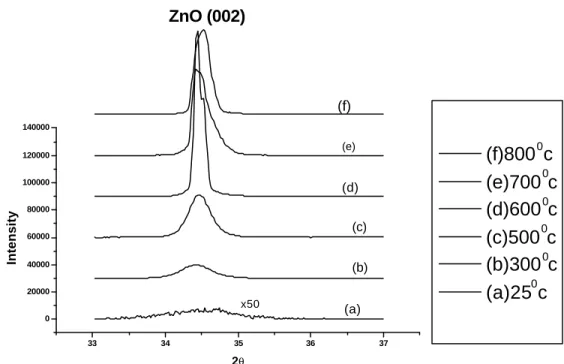
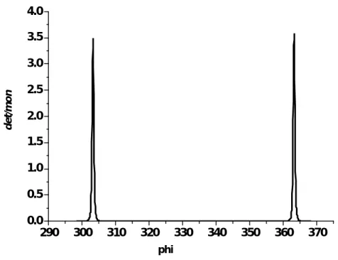
(19) Chapter 4 Results and Discussion 4.1 Results of the XRD measurement. 4.1.1 Growth temperature dependent crystallinity of the ZnO films Fig.4-1 shows XRD patterns of ZnO films deposited by L-MBE at the substrate temperatures of (a) 25, (b) 300, (c) 500, (d) 600,(e) 700, and (f) 800℃. These samples were grown at the repetition rate, laser fluence, and growth rate of 2Hz, 7J/cm2, and 1.2Ao /s, respectively. We found the X-ray θ—2θscan of the ZnO films grown at various temperature are strongly c-axis orie nted, even for the sample grown at room temperature (RT) that exhibit only the (0 0 0 2) peak at 34.4° and (0 0 0 4) peak at 72.5°.. The film grown at 600℃ was found having highest (0 0 0 2) XRD. peak intensity and the smallest full width at half maximum (FWHM). Further increase of the substrate temperature, the peak intensity decreases accompanied increase of FWHM that is possibly due to the re-evaporation of the grown ZnO film at high temperature. The in-plane polar angle F scan was also employed to study the symmetry of the wurtzite structure for some samples. Because the peaks are discrete and separate of 60o , we only scanned two of them to survey six- fold symmetry of ZnO thin film. For the sample grown at 600℃, only the six symmetry equivalent (1 0 1 1) peaks are observed, indicating the film was grown epitaxially by LMBE. Moreover, it was also found that the (1 1 0 0) plane of ZnO is parallel to the (1 2 1 0) plane of sapphire, which corresponds to a 30° rotation of unit cell between ZnO and sapphire. For obtaining the accurate FWHM of the sample, the double-crystal X-ray. - 19 -.
(20) diffraction measurement (DCXRD) was performed for the ZnO sample grown at 600 ℃ by Bede D1 diffractometer. As shown in Fig.4-3, the asymmetrical feature in this data may be related to the inhomogeneous strain in the interface region, which is caused by the large lattice mismatch between ZnO and sapphire (∼18%)11).. The. FWHM is estimated to be 299 arcsec from the data. The relatively low FWHM of the sample shows that good crystal quality of ZnO film can be obtained by L-MBE in high vacuum. It is worth mentioning that the plasma density in the plume might be expected from the Beer’s law that is given by I =Io exp(-Ps x), where Io , P, s , and x are the initial plasma density, the chamber pressure, the cross section for plasma-to-ambient molecule collisions, and the distance from the target, respectively20). The inelastic collisions between ambient molecules and the (Zn, O) plasma that is produced by the ablation of the laser beam, are greatly reduced due to the low chamber pressure.. Hence, the relative density ratio of Zn and O atoms in. the laser-induced plume may be ideally one for the epitaxy in high vacuum.. 4.1.2 Thermal annealing of ZnO films The post thermal annealing, which includes in-situ annealing and post furnance annealing were introduced to enhance the quality of ZnO thin films. The Fig. 4-4 shows the in-plane F scan data of the ZnO film grown at 600℃ and in-situ annealing temperature was 700℃ and annealed about 1hr. The intensity of these diffraction peaks are not equal possibly related to the slight mis-alignment of ZnO c-axis with the rotation axis.. Regardless the imperfection in alignment, the data elucidated that our. ZnO films were grown epitaxially at 600℃ with or without the in-situ thermal annealing. The FWHM of the ZnO (0 0 0 2) diffraction peak measured by DCXRD is estimated to be 217 arcsec. It means that the crystallinity has been greatly improved. - 20 -.
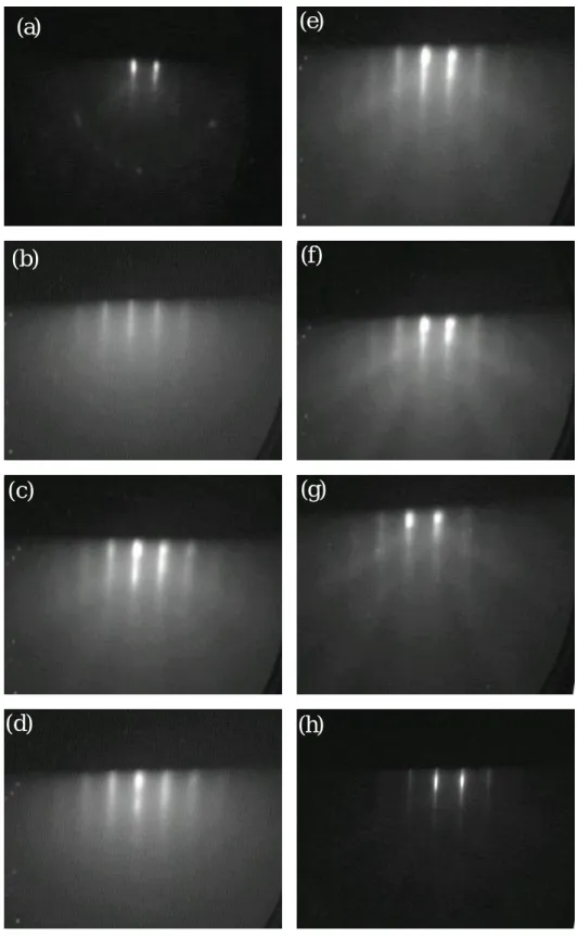
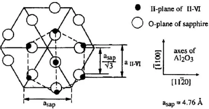
(21) after thermal annealing. The thermal annealing could reduce the defect density and restructure the crystality of the ZnO thin film. If the annealing temperature is too high O2 will re-evaporate and increase the oxygen vacancies. We also used different annealing methods, such as in-situ annealing and post furnace annealing in O2 atmosphere and found in-situ annealing method shows better effect than post annealing method because the in-situ annealing induces less deep- level emission than the post-annealing does. We will discuss this phenomenon in the next section.. 4.2 RHEED observation Fig. 4-5 shows the RHEED patterns observed during the epitaxial growth. Before the deposition, the sapphire substrate shows a sharp streaky pattern [Fig. 4-5 (a)], which indicates a clean and perfect crystalline surface.. Fig. 4-5(b) indicates an. initial incommensurate growth of ZnO on sapphire in a two dimensional (2D) nucleation mode, although the lattice mismatch is as large as 18% for this heteroepitaxial system. The epilayer and the sapphire substrate have been investigated. The [2 1 1 0] orientation of ZnO aligns with the [1 1 0 0] direction of sapphire (Fig. 4-6). This rotation of the crystal orientation of the ZnO epilayer against the substrate occurs because the ZnO lattice aligns itself with oxygen sublattice in sapphire; with this, the lattice mismatch is reduced from around 32% to 18%. However, we should note here that these streaky patterns are quite diffuse [Fig. 4-5 (b)], a feature, which corresponds to small coherent sizes of 2D ZnO islands. Considering the large lattice mismatch, this might be caused by a high density of structure defects and an inhomogeneous strain buildup in the first few monolayers of ZnO. Subsequent growth results in a gradual change of the RHEED patterns from streaky to spotty as shown in Fig. 4-5(a)-(g). This indicates a roughening of the growth surface. No further changes of the rod spacing were observed throughout the - 21 -.
(22) growth.. This morphology evolution is related to a transition of the epitaxial growth. mode from 2D nucleation to three dimensional (3D) nucleation27).. After the. beginning of the growth, the RHEED pattern maintains streaky features until lattice strain relaxation took place at 8 nm. At the onset of strain relaxation, the RHEED pattern becomes spotty, indicative of the formation of islands.. The spotty pattern. continues until the end of the growth with gradual relaxation of lattice strain as shown in Fig. 4-5.. The critical thickness for relaxation of misfit strain is estimated to be. approximately 70 A, based on the findings of Fischer et al.,28,. 29). .. It is worth. mentioning that the spotty RHEED pattern of the relaxed layer can be transformed into a streaky one by in-situ annealing at 700℃ [Fig. 4-5(h)].. 4.3. Result of AFM. 4.3.1 The AFM image for ZnO with different temperature Fig. 4-7(a) ~ (f) illustrate the surface roughness and morphology over an area of 1x1 µ m2 measured by AFM for the ZnO samples grown at different temperatures. The ragged particulates were observed for these samples. It is because that the growth mode was transformed from two-dimensional to three-dimensional growth (Stranski-Krastanov or SK growth) shown in Fig. 4-8, which presumably results from the large lattice mismatch (18%) between ZnO and sapphire as shown in Fig. 4-9. But the mechanism of the 2D nucleation to 3D nucleation transition found in ZnO growth is different form the usual SK growth mode. previous RHEED patterns.. This is further confirmed by. The surface roughness under various growth. temperatures was shown in Table 4-1.. We found the surface (root-mean-square). roughness of the sample grown at 600℃ was determined to be 1.485 nm.. - 22 -.
(23) 4.4 Photoluminescence spectra of ZnO films 4.4.1 Photoluminescence spectra of as-grown films The PL measurements of the ZnO epilayers show that the emission properties vary from sample to sample, even though they were grown under nominally similar conditions. However, the main features of the PL spectra at room temperature are similar for all samples, and can be divided into three categories: the near band edge (NBE) emission, the low energy tail extending from the near band edge emission, and the deep- level emission at room temperature as shown in Fig. 4-10. The typical thickness of ZnO films are 1 µ m. The room temperature PL shows only the near band-edge emission with a peak intensity located at 3.3 eV for the all samples grown at various temperatures (RT ~ 800℃).. The highest peak intensity of band-edge. emission was obtained for the sample grown at 600℃ that is consistent with our earlier X-ray data. The X-ray diffraction pattern shows the FWHM of 0.08o for (0 0 0 2) orientation measured by DCXRD. The FWHM of the band-edge emission for this ZnO film was estimated to be 84 meV (RT), which is relatively small compare to other reports. 21) The near band-edge emission intensity of all samples shown in Fig. 4-10 is not very strong, possibly due to the dislocations or defects caused by the lattice mismatch between ZnO and c-face sapphire.. These dislocations and defects. could act as nonradiative centers, which reduce the intensity from the band-edge emission.. We can anneal the sample of ZnO to reduce these dislocations and. nonradative centers. Fig. 4-11 displays the low-temperature (10K) PL spectra of the ZnO film grown at 600℃. The band-edge emission including the emissions from the free exciton recombination located at 3.379 eV and the dominant peak (3.362 eV), with a FWHM of 5 meV, which is attributable to a transition from an exciton bound to. - 23 -.
(24) a neutral shallow donor (I7 line). The low energy extending tail of the band edge is attributable to emission from the longitudinal phonon replicas (LO) of free exciton (EX) and donor bound exciton (Do X), as shown in the inset of Fig. 4-11. In addition, there is an additional weak broad peaks centered at 2.97 eV, which can be determined as the natural donor-acceptor pairs recombination from the of laser power-dependent PL measurement. The spectrum also included a weak broad band with a peak at 2.23 eV, known as a deep-level emission, which is related to the oxygen vacancy.. 22). We. consider that the generation of oxygen vacancy in ZnO is due to the oxygen nonstoichiometry during the ablation and it should be more serious in our sample due to the lack of oxygen supply. However, our data shows that the intensity of the deep-level emission is more than two orders of magnitude less intense than the exciton emission.. It is suggested that the oxygen deficiency in our sample is. minimized, even in high vacuum. In other words, the ratio of ablated Zn and O element in the laser- induced plume and onto the substrate may be nearly ideal in high vacuum. To further improve the performance of our ZnO films, in-situ annealing (vacuum) and post-furnace annealing (oxygen atmosphere) are suggested.. 4.4.2 Photoluminescence result of the annealed ZnO films By DCXRD, the FWHM of non-annealing ZnO film under a condition of laser energy density ~7 J/cm2 at 2Hz rep. rate and growth temperature 600℃ is 299 arcsec and after annealing it reduce down to 217 arcsec. Now we try to use different annealing method and different annealing temperature to observe the ZnO film properties. First, we used the post- furnace annealing. Fig. 4-12(a)~(d) show PL spectra measured at room temperature of the ZnO films annealed at different temperature and different annealing time in furnace in O2 ambient and the non-annealed ZnO film under a condition of laser energy density 7J/cm2 and growth - 24 -.
(25) temperature at 600℃.. We observed two emission bands from all samples in. Fig.4-12 (a)~(d). One emission band is near band-edge emission at UV range that is attributed to free-exciton recombination, and the other one is visible light emission, which is produced by transition of exc ited optical center from deep level to valence band, and such deep-band emission is usually accompanied by the presence of shallow donors (oxygen vacancies) and deep acceptors (Zn interstitial). Fig. 4-12 (a) ~(d) also show that no matter what the annealing temperature and time the PL intensity is improved after annealing. It is well known that the intensity of light emission was determined by the radiative and nonradiative transition.. The. luminescence efficiency of the light emission can be described by the following formula: ? = WR / (WR + WNR ), where ? is the luminescence efficiency, WR and WNR are radiative and nonrradiative transition probabilities, respectively. Therefore, many lattice defects and surface defects are contained in the as-grown ZnO film. nonradiative centers to reduce light emission.. These defects produce various. As long as the annealing time is too. long the deep- level emission is enhanced rapidly no mater what annealing temperature is. That the deep- level emission becomes strong is a result of increasing the oxygen vacancies or Zn interstitial.. These phenomena also occur when the. annealing temperature is too high in Fig. 4-12 (c)~(d).. Therefore, at high. temperature the defects may be formed in the film by re-evaporation of the O2 molecule, and following reactions may occur at high temperatures: ZnO → ZnZn +Vo +1/2 O2 ZnO → Znj + 1/2O2 As a result, both Znj and Vo act as donors. In addition to re-evaporation of O2 molecule, formation of the spinel layers at the interface between the sapphire - 25 -.
(26) substrate and the ZnO epitaxial layer by higher temperature annealing may also be the cause of the degradation of ZnO layers. From Fig. 4-13, we found the biggest ratio of near band edge emission (NBE) to the deep level emission at annealing temperature 800℃ in furnace with O2 ambient. 4-13.. The best ratio is about 52 in Fig.. Fig. 4-14 indicates the different annealing time at the same temperature 800℃. in furnace with O2 ambient. From Fig. 4-13 and Fig. 4-14, we found the best annealing temperature and time are 800℃ and 1hr in our experimental system. The above-mentioned method is the furnace annealing with O2 ambient. We also used the in-situ annealing to improve the structure of ZnO. Fig. 4-15 indicates the PL spectra of in-situ annealed ZnO films at 700℃ and different annealing time and the non-annealed ZnO film under a condition laser energy density 7J/cm2 at 2Hz rep. rate and growth temperature 600℃. We can easily observe the NBE intensity is strong after annealing 1hr. The intensity ratio at RT of near band edge emission to deep- level emission is 48 in Fig. 4-15. emission with FWHM is 60meV.. The near band-edge. Compared to the post-annealing method, the. in-situ annealing will induce less O vacancies even in the long annealing time. We guessed that the thermal force is a major reason because the post-annealing in furnace is quasi-rapid thermal annealing (RTA). The force may cause O molecule evaporate rapidly.. So the optimal condition for in-situ annealing is 700C for 1hr under high. vacuum P=10-9 torr.. In-situ annealing is a better choice because the less O vacancies. will be induced. Fig. 4-16 shows photoluminescence spectra from the ZnO thin film at 10K and the film grown at 600℃ and in-situ annealing at 700℃ for one hour. The inset in Fig. 4-16 shows, in a logarithmic scale, the NBE emission at 10K. The dominant peak at 3.364eV is from the exciton bound to neutral donors (Do X) transition. The FWHM of peak is around 4 meV. The low energy extending tail of the band edge is attributable to emission from the longitudinal phonon replicas (LO) - 26 -.
(27) of free exciton (EX) and donor bound exciton (Do X), as shown in the inset of Fig. 4-16. Table.4-2 shows the mechanism and the positions of spectral peak. Fig. 4-17 shows emission spectra of the ZnO film in the temperature range from 10 ~ 300 K. At low temperature, the spectra are dominated by the neutral-donor bound exciton emission at 3.364 eV. With increasing temperature, the bound exciton emission decreases rapidly, and is hardly resolved above 140 K. At around 70 K the acceptor bound exciton vanishes. At the onset of bound exciton decay, a feature at 3.378 eV becomes stronger and finally dominates the spectra even up to room temperature.. The feature is assigned to free exciton emission due to its narrow line. width and the temperature dependence of its intensity. Fig. 4-18 plots the positions of the exciton emission up to 295 K. Similar plots have been reproduced from D. M. Bagnall et al. 23). We performed numerical. analyses of the energy position of the free exciton as function of temperature using a model, a modification of Varshni equation for the band gap temperature dependence: E(T) = E(0) -. αT 4 . (β + T )3. (1). A band gap value obtained from Eq (1) fitting to the Fig. 4-16(a) gives 3.37752 eV. Similar energy band gap ( E0 =3.3801 eV) been produced from Boemare et al. 25,26) In Ref. [24] the authors suggest a semi-empirical expression equivalent to the Bose-Einstein model proposed by Ref. [25] that provides us with fitting and an estimative of the Debye temperature.. Eq.(2) gives the best fitting to the data. Fig.4-16(b), with a Debye temperature of TD=3/2T=550K, where T is the effective phonon temperature. The different values of the parameters are given in the inset of Fig. 4-16(b). E (T ) = E( 0) −. αΘ exp( Θ / T ) − 1. Eq. (2). It indicates that we have determined the temperature dependence of the free exciton - 27 -.
(28) peak position in the high-textured ZnO film in good agreement with the literature.25) Within a Frank-Condon model26), the coupling of the exc iton transition to the LO phonon is expresses by the exciton-phonon coupling constant, S. The intensity distribution of the phonon replicas is determined by S. For the case of relatively strong coupling, the emission intensity of the nth phonon replica In (?) and the principle emission line (Io) is related by I n = Io. S n e−s n!. n=0, 1, 2… ... From the Fig. 4-16, we can found the S factor to be 0.213 for free exciton and 0.0136 for the donor bound exciton at n=1. From the S factor, we know the free exciton couple phonon stronger than the neutral donor bound exciton.. 4.5 Optical transmittance spectra of ZnO thin film In order to avoid scattering problem in the transmittance measurement, the ZnO thin film was grown on two-side polished sapphire substrate. As shown in Fig. 4-19, the transmittance was higher than 90% in the visible region but with a steep falloff at 380 nm, which is related to the band-gap absorption in ZnO material (3.3 eV).. 4.6 Other properties of ZnO film Room-temperature Hall measurement was also performed to study the electrical properties of the ZnO films. We use the Van der Pauw method to measure the Hall effect and use the indium (In) ball as ohm contact. The carrier concentration and the mobility for the sample grown at 600℃ are 1.8 ×1017 cm—3 and 16 cm2 /V•sec, respectively.. The carrier concentration and mobility is similar to the best result. reported for the film prepared using oxygen atmosphere and an additional buffer layer. For the ZnO sample prepared by in-situ therml annealing, the mobility increased up to - 28 -.
(29) 27 cm2 /V•sec and the concentration down to 1 ×1017 cm—3 . In other words, the structure of ZnO become improves and defects decrease after thermal annealing.. - 29 -.
(30) Chapter 5. Conclusion and perspectives. 5.1 Conclusion High quality ZnO thin films have been fabricated on c-face sapphire by laser-MBE equipped with KrF excimer laser. From the DCXRD analysis, the optimum growth conditions for the preparation of ZnO films are with growth temperature Ts=600℃ and in-situ annealing temperature T=700℃.. ZnO films of. (002) peak with a FWHM of 0.06o were obtained with laser energy density flux of 7J/cm2 at these conditions. The target-substrate distance and repetition rate of the KrF laser are 50mm and 2Hz, respectively.. The thin film thickness measured by. surface profile was around 1µm. From the room temperature PL, the free exciton emission is dominant and the FWHM is 60meV. From low-temperature PL. there are the presence of donor-bounded and free exciton which has LO-phonon replicas.. The FWHM of. dominant peak is 4meV. With increasing the temperature, the donor-bounded exciton decays and free exciton finally dominant the spectra up to room temperature. In-situ annealing is the better choice than post- thermal treatment because the less O vacancies would be induced. fitting give 3.377 eV.. A band gap value obtained from Vaeshni formula. The transmittance data was shown to be higher than 90% in. the visible region. The lowest surface roughness measured by AFM was 1.4nm. The mobility is 27 cm2 /V•sec and the concentration is 1 ×1017 cm—3 after in-situ annealing.. 5.2 perspectives In this research, our major objective is to fabricate high quality ZnO thin - 30 -.
(31) films by laser-MBE and to analyze its optical properties.. We have grown. high-quality ZnO films on sapphire without flowing oxygen. In the future, we will work on different substrate such as Si and GaN substrate. Moreover, we can deposit Er doped ZnO film using the former experience and analysis methods, for studying electro-luminescence property of Er doped ZnO material in the future.. - 31 -.
(32) References 1). Bixia Lin and Zhuxi Fu, Yunbo Jia, Appl. Phys. Lett. 79, 943, 2001. 2). Gregory J. Exarhos, Shiv K. Sharma, Thin Solis Film 270 (1995) P. 27-32. 3). Jpn. J. Appl. Phys. 38, (1999) 5192. 4). Yefan Chen, D. M. Bahnall, Hang-jun Koh, Ki-tae Park, Kenji Hiraga, Ziqiang Zhu, and Takafumi Yao, J. APP. PHY. Volume 84, number 7, 1 october 1998. 5). Bagnall DM, Chen YF, Zhu Z, et al. APPL PHYS LETT 70 (17): 2230-2232 APR 28 1997 6). M. Kawasaki, Y. Segawa et al. Phys. Stat. Sol (b) 202, 669 (1997) 7). J. Alloys & Comp. 219 (1995) 93. 8). K. Ogata, T. Kawanishi, K. Maejima, K. Sakurai, Shizuo Fujita and Shigeo Fujita: Jpn. J. Appl. Phys. 40 (2001) L657. 9). V. Cracium, J. Elders, J. G. E. Gardeniers and lan W. Boyd: Appl. Phys. Lett. 65 (1994) 2963. 10). I. Yamauchi, S. Ueyama and I. Ohnaka: Mater. Sci. Eng. A 208 (1996) 108. 11). I. Yamauchi, S. Ueyama, and I. Ohnaka: Mater. Sci. Eng. A 208 (1996) 101. 12). I. Yamauchi, A. Suganuma, T. Okamoto and I. Ohnaka: J. Mater. Sci. 32 (1997) 4603 13). H. Shibata, Y. Makita, H. Kakemoto, Y. Tsai, S. Sakuragi, H. Katsumata, A. Obara, N. Kobayashi, S. Uekusa, T. Tsukamoto, T. Tsunoda and Y. Imai: Proc. 15th Int. Conf. Thermoelectrics, 1996 (IEEE, Piscataway, NJ, 1996) p.62 14).Rajiv K, Singh and J. Narayan, Phys. Review. B, 41, 8843, 1990. 15).K.Y. Cheng, Proceedings of the IEEE, (85),NO.11,1997. - 32 -.
(33) 16).Optical characterization of semiconductors: infrared, Raman, and Photoluminescence spectroscopy (Sidney Perlpwotz, USA, 1993) p.61 17).Optical Processes in Semiconductors , Jacques I. Pankove, Nw York, 1971, P.107. 18).Semiconductor Optics C.F. Klingshirn P.281 19). D. H. Tassis, C. A. Dimitriadis and O. Valassiades: J. Appl. Phys.84 (1998) 2960. 20.) G. R. Lin, W. C. Chen, C. S. Chang and C. L. Pan: Appl. Phys. Lett. 65 (1994) 3272. 21). H. Kakemoto, Y. Makita, H. Katsumata, T. Iida, C. Stauter, A. Obara, H. Shibata, Y.S. Tsai, S. Sakuragi, N. Kobayashi, M. Hasegawa, S.I. Uekusa and T. Tsukamoto: Proc. SPIE 2888 (1996) 32. 22). Thermoelectricity ed. P. H. Egli (John Wiley & Sons, Inc., New York & London, 1960). 23). D. M. Bagnall, Y. F. Chen, M. Y. Shen, Z. Zhu, T. Goto, and T. Yao, J. Crys.Growth, 184/185, P.605-609, 1998 24). R.Passler, E. riebl, H. Rielp, G. Lautner, S. Bauer. H. Preis, W. Gabhardt, J. Appl. Phys. 86 (1999) 4403 25). L.Vina, Logothetidis, M.Cardona, Phys. Rev. B 30 (1984) 1979 26). C. Boemare, T. Monteiro, M.J. Soares, J.G. Guilherme, E. Alves, Physica B 308-310 (2001) 985-988 27). Yefan Chen, D.M. Bagnall, Hang-jun Koh, Ki-tea Park, Kenji Hiraga, Journal of App. Physics Vol. 84, 7,1998. 28). Hang-Ju Ko, Soon-Ku Hong, Yefen Chen, Takafumi Yao, Thin Solid Films 409 (2002) 153-160 29). A.Fischer, H Kulme, H. Richter, Phys. Rev. Lett.73 (1994) 2721.. - 33 -.
(34) Fig.2-1 (a) System layout and (b) the load lock chamber and (c) main chamber. - 34 -.
(35) Fig.2-2 Schematic diagram of the RHEED geometry. This shows a glancing incidence beam of electrons at an incident angle ? and an azimuthal angle f upon a surface plane.. - 35 -.
(36) KrF excimer laser 248nm. Laser beam. Mirror scanner Focus lens f=40cm RHEED Screen. Mass Sample exchange chamber. Gate. spectrometer Viewport. Heater. valve. Target Substrate Main RHEED. chamber. Gun. Fig.3-1 Laser-MBE system. - 36 -. Pressure ion gauge.
(37) ZnO (002). (f) 140000. 100000. Intensity. 0. (e). 120000. (f)800 c 0 (e)700 c 0 (d)600 c 0 (c)500 c 0 (b)300 c 0 (a)25 c. (d). 80000. (c). 60000 40000. (b). 20000. x50. (a). 0 33. 34. 35. 36. 37. 2θ. Fig. 4-1(a) XRD of ZnO films grown at different temperature at 2pulses/sec. The diffraction Bragg peak at 34.4o is the ZnO (002) peak.. 0.45 120000 100000. 0.35. 80000. 0.30. 60000. 0.25 0.20. 40000. 0.15. 20000. 0.10. 0 300. 400. 500. 600. 700. 800. Temperature(o C). Fig. 4-1(b) The ZnO (002) peak and intensity vs. growth temperature.. - 37 -. (002) peak int.(a.u). FWHM (delta degree). 0.40.
(38) 4.0 3.5. det/mon. 3.0 2.5 2.0 1.5 1.0 0.5 0.0 290. 300. 310. 320. 330. 340. 350. 360. 370. phi. Fig.4-2 F scan of the ZnO thin film growth at 600℃. The Bargg. Intensity(a.u.). diffraction peak is ZnO (1 0 1 1) peak.. 10. 4. 10. 3. 10. 2. 10. 1. FWHM=299arcsec. -4000. -2000. DCXRD. 0. 2000. 4000. th(arcsec) Figure 4-3. The double-crystal X-ray diffraction pattern of ZnO film grown directly on c-face sapphire at 600℃. The Bargg diffraction peak is ZnO (002) peak.. - 38 -.
(39) 7 6. det/mon. 5 4 3 2 1 0 -1 0. 50. 100. 150. 200. 250. 300. 350. phi Fig. 4-4 F scan of the ZnO thin film growth on temperature 600℃ and in-situ annealing at 700℃ for 1hr.. The Bargg diffraction peak is ZnO (1 0 1 1) peak.. - 39 -.
(40) (a). (e). (b). (f). (c). (g). (d). (h). Fig. 4-5 RHEED patterns of (a) the sapphire substrate after thermal treatments and ZnO epilayer after the deposition of about (b) 2, (c)8, (d)40, (e)100, (f)300, (g)1000 nm. The growth temperature for this sample is 600℃. (h) The pattern is under in-situ annealing 700℃ for 1hr. - 40 -.
(41) Fig.4-6 Schematic diagram showing the epitaxial relationship of ZnO(0001) grown on Al2 O3 (0001).. - 41 -.
(42) Ts=25℃ RMS~3.4nm. Ts=300℃ RMS~1.8nm. Ts=500℃ RMS~1.8nm. - 42 -.
(43) Ts=600℃ RMS~1.4nm. Ts=700℃ RMS~1.7nm. Ts=800℃ RMS~2.7nm. Fig. 4-7. The morphology of ZnO films at different growth temperature. - 43 -.
(44) Fig. 4-8. Stranski-Krastanov growth. Fig. 4-9 Diagram of the lattice mismatch between ZnO and sapphire. - 44 -.
(45) Table4-1 Growth temperature (o C). 25. 300. 500. 600. 700. 800. surface roughness (root-mean-square)(nm). 3.4. 1.8. 1.8. 1.4. 1.7. 2.7. Substrate:sapphire. Intehsity. o T=800 C o T=700 C. 1400 1300 1200 1100 1000 900 800 700 600 500 400 300 200 100 0 -100 350. o T=600 C o T=500 C o C. T=300. o. T=25 C 400. 450. 500. 550. 600. Wavelength(nm). Fig. 4-10 PL spectra of ZnO films grown at different growth temperatures, freq. rate of 2Hz, the deposition time for 2hr.. - 45 -.
(46) PL Intensity (a. u.). PL Intensity (a. u.). 10K 10. DoX. o FWHM=5 meV D X 10K. 4. EX 103. 10. DoX- 1LO D0 X- 2LO EX- 1LO. 2. EX- 2LO 3.2. 3.3. 3.4. Photon Energy (eV). X10. 1.6 1.8 2.0 2.2 2.4 2.6 2.8 3.0 3.2 3.4 3.6 Photon Energy (eV). Fig. 4-11 photoluminescence spectra at 10 K showing near band-edge (NBE), grew at the temperature 600℃, freq. rate 2Hz in deposition time 2 hr under high vacuum 10-9 torr. Inset shows detailed view of NBE emission.. - 46 -.
(47) (a). @RT. PL Intensity(a.u.). 2000. o. 700 C annealing unannealed 30min 60min 120min. 1500. 1000. 500. 0 350. 400. 450. 500. 550. 600. 650. 700. Wavelength(nm). (b). @RT. 25000 o. 800 C annealing 5min 10min 30min 60min 120min 180min unannealed. PL Intensity(a.u.). 20000 15000 10000 5000 0 350. 400. 450. 500. 550. Wavelength(nm). - 47 -. 600. 650. 700.
(48) (c). @RT. PL Intensity(a.u.). 25000. o. 900 C annealing unannealed 60min 120min. 20000 15000 10000 5000 0 350. 400. 450. 500. 550. 600. 650. 700. Wavelength(nm). (d) 40000. @RT. PL Intensity(a.u.). 35000 30000 25000 20000. o. 1000 C annealing unannealed 60min 120min. 15000 10000 5000 0 350. 400. 450. 500. 550. 600. 650. 700. Wavelength(nm). Fig. 4-12 The PL spectra of annealed ZnO films at different temperature and different annealing time by furnace. The non-anneal ZnO film under a condition laser energy density 7J/cm2 at 2Hz rep. rate and growth temperature 600℃. - 48 -.
(49) 60 50. Ratio. 40 30 20 10 0 700. 800. 900. 1000. temperature(oC). Fig. 4-13 The emission intensity ratio (near band-edge emission to deep-level emission) of the ZnO annealed at different temperature for 1hr and measured at room temperature.. 30000 NBE Intensity Deep-Level intensity. 1hr. 25000. intensity. 20000 15000 10000 5000 0. 0. 20. 40. 60. 80. 100 120 140 160 180 200. anneal min. Fig. 4-14 PL spectra of ZnO films for different annealing time at the same temperature 800℃ by furnace in O2 ambient.. - 49 -.
(50) unannealed o in-situ annealing 700 C 1hr o in-situ annealing 700 C 3hr. 20000 18000 16000. Intensity. 14000 12000 10000 8000 6000 4000 2000 0 350. 400. 450. 500. 550. 600. 650. 700. 750. Wavelength(nm). Fig. 4-15 shows the PL spectra of in-situ annealed ZnO films at 700℃ for different annealing time. The non-anneal ZnO film under a condition laser energy density 7J/cm2 at 2Hz rep. rate and growth temperature 600℃.. - 50 -.
(51) DoX. 4meV o D X-LO DoX-2LO o D X-3LO 72meV o A X 72meV 71meV. EoX. 65meV o E X-LO 72meV Eo X-2LO 72meV o E X-3LO. 3.0. 3.1. 3.2. 3.3. 3.4. eV. 1.6. 1.8. 2.0 2.2. 2.4. 2.6. 2.8. 3.0. 3.2 3.4. 3.6. eV Table 4-2 Spectrum Mechanism. Free EX. Do X. Ao X. Free EX-LO. Do X-LO. Position(eV) Spectrum Mechanism. 3.378 Free EX-2LO. 3.364 Do X-2LO. 3.33414 Free EX-3LO. 3.3124 Do X-3LO. 3.2916. Position(eV). 3.24. 3.219. 3.167. 3.149. Fig. 4-16 photoluminescence spectra at 10 K showing near band-edge (NBE), grew at 600℃ with in-situ annealing 700℃ for 1hr under high vacuum 10-9 torr. Inset shows detailed view of NBE emission. The table 4-2 lists the mechanism and position of spectrum.. - 51 -.
(52) 300K. 200K. 180K. Log sacale(a.u). 100000. 10000. 100K. 1000. 50K. 10K. 100 3.2. 3.3. 3.4. 3.5. Energy(eV). Fig. 4-17 Emission spectra of the ZnO thin film in the temperature range 10-300 K.. - 52 -.
(53) (a) 3.38 3.37 3.36. Eg(eV). 3.35 3.34. Varahni equation 4 3 E(T)=E(0)-αΤ /(β+Τ). 3.33 3.32. Ε(0)=3.37752 eV α=0.007 meV/K β =118 K. 3.31 3.30 0. 50. 100. 150. 200. 250. 300. 250. 300. Temperature(K). (b). 3.38. Eg(eV). 3.36. 3.34. 3.32. E(T)=E(0)-αθ/(exp(θ /T)−1) E(0)=3.37629eV α=0.49 meV/K θ =366.94 K. 3.30 0. 50. 100. 150. 200. Temperature(K) Fig. 4-18(a) Evolution of the energy position of the free exciton as function of temperature ( ) data, (-) the fittings using the Eqs.(1) and (b) use the Eqs.(2). - 53 -.
(54) 100 90. Transmittance(%). 80 70 60 50 40 30 20 10 0 200. 300. 400. 500. 600. 700. 800. 900. Wavelength(nm). Fig. 4-19 The transmittance spectra of ZnO. The ZnO growth condition was at 600℃ with in-situ annealing at temperature 700℃ for 1hr.. - 54 -.
(55)
數據

+4


相關文件
The resulting color at a spot reveals the relative levels of expression of a particular gene in the two samples, which may be from different tissues or the same tissue under
identify different types of tourist attractions and examine the factors affecting the development of tourism in these places;.4. recognize factors affecting tourist flows and the
Akira Hirakawa, A History of Indian Buddhism: From Śākyamuni to Early Mahāyāna, translated by Paul Groner, Honolulu: University of Hawaii Press, 1990. Dhivan Jones, “The Five
Proceedings of IEEE Conference on Computer Vision and Pattern Recognition, pp... Annealed
To decide the correspondence between different sets of fea- ture points and to consider the binary relationships of point pairs at the same time, we construct a graph for each set
This study, analysis of numerical simulation software Flovent within five transient flow field,explore the different design of large high-temperature thermostat room
4: Damage (in Bytes) caused by 200-second large flows at different average flow rate R atk (in Byte/s) and duty cycle θ = 1.0 (flat large flows) under de- tection of different
在慢速乾燥填補了 ZnO 奈米柱和 Polymer 的間距,因為延長了乾燥 時間,溼膜有很長時間有效滲入 ZnO
