Interfacial Reactions of Liquid Sn and
Sn-3.5Ag Solders With Ag Thick Films
T.L. Su, L.C. Tsao, S.Y. Chang, and T.H. Chuang (Submitted 28 March 2002)
The interfacial reactions of liquid Sn and Sn-3.5Ag solders with Ag thick films are investigated in the temperature range from 250-325 °C, and the morphology of intermetallic compounds formed after such soldering reactions is observed. In kinetics analysis of the growths of intermetallic compounds, it was found that both Sn/Ag and Sn-3.5Ag/Ag reactions were interfacial-controlled, and the growth rates for both cases were similar. The rate of Ag dissolution into liquid solder attendant on the formation of interfacial intermetallic compounds after Sn/Ag reaction was about four times higher than that after Sn-3.5Ag/Ag reaction, as evidenced by experimental results.
Keywords Ag dissolution, Ag3Sn intermetallic compound, Ag
thick film, Sn/Ag, Sn-3.5Ag/Ag, soldering reactions
1. Introduction
In a previous work by the authors, the intermetallic com-pounds and their growth kinetics during the soldering reactions between liquid Sn and Ag plates were studied.[1] The results
showed that, along with the formation of Ag3Sn intermetallic
compounds at Sn/Ag interface, the Ag substrate dissolved se-verely into the molten solder. Typically, such an erosion phe-nomenon on the Ag substrate can be alleviated by the addition of the Ag element into the Sn solder, in which case the growth kinetics of interfacial intermetallic compounds will also be affected. Because Ag thick films have been widely used for the manufacturing of hybrid integrated circuits (HIC), resistors, ceramic capacitors, and multilayer chip inductors, it makes sense to conduct a further investigation of Sn and Sn-Ag sol-ders reacted with Ag thick films. For the present experimental investigation, a eutectic Sn-3.5Ag alloy was used, which has been recognized as one of the promising candidates for Pb-free solders in the electronics industry. This study compared the growth kinetics of interfacial intermetallic compounds and dis-solutions of Ag thick films between Sn/Ag and Sn-3.5Ag/Ag soldering reactions.
2. Experimental
For the preparation of the Ag thick film, the surface of an alumina substrate was coated with silver paste (composition: Ag 75-80 wt.%, glass 1-5 wt.%, resin 1-5wt.%, Terpineol 5-10 wt.% and Diethyl Phthalate 5-10 wt.%) using a screen printer. Specimens were first heated at 150 °C for 10 min and then sintered at 850 °C for 10 min in an air furnace. After the specimens were sintered, they were cooled to room
tempera-ture. The sintered Ag thick film on the alumina substrate pos-sessed a thickness of 10m and low porosity. The Sn-3.5Ag solder was prepared by vacuum melting into an ingot and ho-mogenized at 100 °C for 50 h. Afterward, both the Sn and Sn-3.5Ag solders were rolled into 0.2 mm thick foils. For the study of interfacial reactions, the solder foil was cut to the same size as the Ag/Al2O3substrate, placed on the Ag/Al2O3 sub-strate, and then heated in an IR furnace under a vacuum of 10−3 torr. To eliminate the oxidation factor in soldering, a flux of SMQ TACFLUX 005 (Indium Co., Utica, NY) was applied before testing.
Soldering reactions took place at temperature ranging from 250-325 °C for various periods of time. After the reaction, the soldered specimens were cut along the cross section, ground with SiC paper, polished with 1 and 0.3m Al2O3powders,
and observed by scanning electron microscopy (SEM). For kinetics analysis, the thicknesses of intermetallic compounds were calculated by dividing the total areas of interfacial inter-metallics by the widths of the interinter-metallics on the micro-graphs. The dissolved thickness (XD) of the Ag thick film was estimated as follows: XD ⳱ XI − XR − X
Ag
IM ⳱ XI − XR −
(3/4)XIM, where XIis the initial thickness of the Ag thick film,
XR is the residual thickness of the Ag thick film, XIMis the
thickness of the interfacial intermetallic compound, and XAg IM
signifies the partial thickness of Ag in the intermetallic com-pound. The intermetallic compound in this study was Ag3Sn as
analyzed by electron probe microanalysis (EPMA). The differ-ence in atomic size between Ag and Sn notwithstanding, the partial thickness (XAg
IM) of the Ag thick film contained in the
Ag3Sn intermetallic compound was about (3/4)XIM.
3. Results and Discussion
The typical micrographs of intermetallic compounds formed during interfacial reactions between liquid Sn and Ag thick films are shown in Fig. 1. It can be seen that the intermetallic compounds at the Sn/Ag interface have a scallop-type mor-phology. EPMA analyses indicate that these interfacial inter-metallic compounds are in the Ag3Sn phase. Through selective
etching out of the Sn solder from the reacted Sn/Ag specimens,
T.L. Su, L.C. Tsao, S.Y. Chang,and T.H. Chuang, Department of Materials Science and Engineering, National Taiwan University, Tai-pei 106, Taiwan, China. Contact e-mail: [email protected].
the Ag3Sn phase is further confirmed by x-ray diffractometry (XRD) to be present in the remaining intermetallic compounds, as shown in Fig. 2. The intermetallic compounds formed during the interfacial reactions of Sn thin film, and Sn-Pb and Sn-Ag solders with Ag substrates, have been reported in the literature to be in the Ag3Sn phase,
[2-8]
which is consistent with the results of the current study.
Figure 1 illustrates that the Ag thick film dissolves into the pure Sn matrix for a distance of about 13m after soldering reaction at 250 °C for 20 min. The dissolved Ag atoms result in the formation of needle-like precipitates near the Ag/Sn interface, which are also shown to be in the Ag3Sn phase as analyzed by EPMA. No Ag3Sn precipitates appear in the Sn
matrix aside from this region. After the soldering reaction at
Fig. 1 Micrographs of the interfacial intermetallic compounds and matrix precipitates formed during soldering reaction between liquid Sn and the Ag thick film. (a) 250 °C, 20 min. (b) 250 °C, 25 min. (c) 250 °C, 30 min. (d) 300 °C, 7 min. (e) 300 °C, 15 min. (f) 300 °C, 18 min
250 °C for 25 min or more, or as the reaction temperature is raised to above 275 °C for various time periods, the Ag3Sn precipitates are seen to distribute fully in the Sn matrix. In this case, the needle-like Ag3Sn precipitates are broken into par-ticles located preferentially at grain boundaries of the Sn ma-trix. Figure 1 also shows that the residual Ag thick film has become porous after the soldering reaction. Such a porous structure of the remaining Ag thick film may be correlated to the severe dissolving of Ag Atoms through the grain bound-aries of the sintered Ag thick film.
The micrographs in Fig. 1 also show that the scallop-shaped Ag3Sn intermetallic compounds at the Sn/Ag interface grow
with increasing reaction temperature and time. As the Sn/Ag soldering reaction approaches the end, a number of large in-termetallic bands appear in the Sn matrix, as shown in Fig. 1(e) and (f). EPMA analyses indicate that their compositions are the same as those of the interfacial Ag3Sn intermetallic com-pounds. From the Ag-Sn phase diagram, it can be seen that these large Ag3Sn intermetallic bands result from the decom-position of liquid solder bearing excessively dissolved Ag at-oms into the Ag3Sn phase (intermetallic bands) and the eutectic phase (Ag3Sn fine particles embedded in the Sn matrix) during
the solidification process. However, a certain amount of inter-metallic bands are found to settle along the Sn/Al2O3interface where the Ag thick film has been consumed (Fig. 1f). It seems that the Ag3Sn intermetallic bands have been preferentially formed ahead of the Sn/Al2O3interface prior to the conclusion
of the Sn/Ag soldering reaction. At that moment, the previously created scallop-shaped Ag3Sn intermetallic compounds are
split away from the remainder of the thin Ag layer, which has been prone to dissolve exhaustively into the liquid Sn solder. The drastically increased Ag concentration in the liquid Sn solder ahead of the Sn/Al2O3interface results in the
preferen-tial decomposition of solder during the solidification process to form the intermetallic bands. These intermetallic bands will float away from the Sn/Al2O3interface into the liquid solder
matrix because of their poor bonding with the Al2O3 ceramic substrate.
The morphology of the interfacial intermetallic compounds formed during the soldering reaction between liquid Sn-3.5Ag
and Ag thick films (shown in Fig. 3) is similar to that during the Sn/Ag soldering reaction. In both cases, there are also simi-lar appearances of precipitates in the solder matrix. However, the precipitate-free region at the early stage of Sn/Ag soldering reaction (Fig. 1a) cannot be found with the Sn-3.5Ag/Ag re-action (Fig. 3a), which indicates that most of the precipitates formed in the latter case have originated from the Ag alloying element contained in the Sn-3.5Ag solder. It also results in a thicker residual Ag thick film after Sn-3.5Ag/Ag soldering re-action at 250 °C for 20 min (Fig. 3a) as compared with the Sn/Ag reaction (Fig. 1a). In addition, the structural porosity of the remaining Ag thick film after Sn/Ag soldering reaction can obviously be alleviated for the Sn-3.5Ag/Ag reaction (Fig. 3). At the final stage of the Sn-3.5Ag/Ag soldering reaction, the floating of large intermetallic bands can also be observed (Fig. 3e, f). Figure 3(e) gives a strong indication that such floating intermetallic bands have been stripped from the solder/Al2O3 substrate interface.
The thicknesses of the interfacial intermetallic compounds (XIM) formed during the soldering reactions of liquid Sn and
Sn-3.5Ag with Ag thick films under various conditions are summarized in Tables 1 and 2. The data are plotted against the
Table 1 Thicknesses of Interfacial Intermetallic Compounds Under Various Conditions (a) T, °C t, min XIM, µm XR, µm X Ag IM, µm XD, µm 250 20 2.2 4.8 1.7 3.5 250 25 4.8 4.1 3.6 2.3 250 30 6.6 3.2 5.0 1.8 275 9 2.3 3.2 1.7 5.0 275 15 5.4 2.8 4.0 3.2 275 20 7.0 1.0 5.2 3.4 300 7 1.6 3.2 1.2 5.6 325 5 2.8 1.6 2.1 6.4
(a) The thicknesses of residual Ag thick Films (XR), created intermetallic compounds (XIM), dissolved Ag thick films (XD), and the partial thickness of Ag in the created intermetallic compounds (XAg
IM) after soldering
reac-tions between liquid Sn and Ag thick films at various temperatures (T) for various times (t)
Table 2 Thicknesses of Interfacial Intermetallic Compounds Under Various Conditions
T, °C t, min XIM, µm XR, µm X Ag IM, µm XD, µm 250 20 2.4 7.9 1.3 0.2 250 28 4.6 5.7 3.4 0.8 250 32 5.6 5.6 4.2 0.3 275 20 2.5 6.3 1.9 1.8 275 24 4.7 5.7 3.5 0.8 275 28 5.5 5.3 4.2 0.6 300 12 4.8 5.7 3.6 0.7
(a) The thicknesses of residual Ag thick films (XR), created intermetallic
compounds (XIM), dissolved Ag thick films (XD), and the partial thickness
of Ag in the created intermetallic compounds (XAg
IM) after soldering
reac-tions between liquid Sn-3.5 Ag and Ag thick films at various temperatures (T) for various times (t)
Fig. 2 Typical x-ray diffraction patterns of the intermetallic com-pounds formed at the interface between liquid Sn and Ag thick film after selectively etching out the Sn unreacted solder
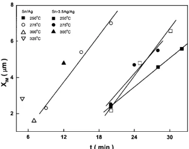
reaction time as shown in Fig. 4. For each soldering tempera-ture in this study, there were fewer than three reliable mea-surements obtained because the as-sintered Ag thick film pos-sesses only a thickness of 10m. Despite insufficient data for kinetics analysis, the plots in Fig. 4 are approximately linear, which implies that the growths of interfacial intermetallic com-pounds during both reactions of Sn and Sn-3.5Ag solders with Ag thick films are interface-controlled. However, in our
pre-vious study on the interfacial reaction between liquid Sn solder and Ag plates, the growth kinetics of Ag3Sn intermetallic com-pounds was shown to be diffusion-controlled.[1] Such a dis-crepancy also appeared in our previous studies on the interfa-cial reactions of In49Sn solder with Ag plates[9]and Ag thick
films.[10]This type of linear growth kinetics of the intermetallic compounds should be attributed to the penetration of liquid solder through the interfacial glass phase between the sintered
Fig. 3 Micrographs of the interfacial intermetallic compounds and matrix precipitates formed during soldering reaction between liquid Sn-3.5Ag and the Ag thick film. (a) 250 °C, 20 min. (b) 250 °C, 28 min. (c) 250 °C, 32 min. (d) 300 °C, 12 min. (e) 300 °C, 16 min. (f) 300 °C, 20 min
Ag grains. The penetrated liquid solder reacts with the Ag grains at their interfaces, which results in an interfacial con-trolled growth of the intermetallic compounds. From Fig. 4, it can also be seen that the growth rates of interfacial interme-tallic compounds during the Sn/Ag and Sn-3.5Ag/Ag soldering reactions are similar.
From Fig. 1 and 3, it can be observed that accompanying the formation of interfacial intermetallic compounds, a large amount of precipitates appear in the solder matrix. For the Sn/Ag reaction, such precipitates in the Sn matrix should result from the dissolution of Ag atoms from Ag thick films into liquid Sn solder. In fact, the dissolution of the Ag substrate during the Sn/Ag soldering reaction has been evidenced
through marking the original Sn/Ag interface with a Ta thin film.[1]Even for the Sn-3.5Ag solder reacted with the Ag thick film, further dissolutions of Ag atoms into the liquid solder are inevitable, though basically the situation can be mitigated to a certain degree. To compare the dissolution of the Ag thick film during the Sn/Ag soldering reaction with that during the Sn-3.5Ag/Ag reaction, the residual thicknesses of Ag thick films (XR) in both cases are measured and listed in Tables 1 and 2.
The difference between the initial thickness (XI) and the
re-sidual thickness (XR) of Ag thick films gives the thickness (XC) of Ag thick films consumed after the soldering reactions. Con-sistent with the growth rate analysis in Fig. 4, the plots for the consumed thickness of Ag thick films as shown in Fig. 5 are also governed by a linear relation.
Because the consumed Ag thick films are used in part to form the interfacial intermetallic compounds and in part to dissolve into the liquid solder, the dissolution amounts of Ag thick films (XD) can be obtained by subtracting the residual Ag thickness (XR) and the partial Ag thickness in the created
Ag3Sn intermetallic compounds (X
Ag
IM) from the initial Ag
thick-ness (XI). It has been known that the lattice size of Ag (a⳱
4.086 Å) is near that of Sn (a⳱ 5.831 Å, c ⳱ 3.181 Å). The partial Ag thickness in the Ag3Sn intermetallic compounds (XAg
IM) can thus be roughly estimated as (3/4)XIM.In Tables 1
and 2, the XDvalues are also shown for Sn/Ag and Sn-3.5Ag/
Ag soldering reactions. It is obvious that the dissolution amounts of Ag thick films during the Sn/Ag reaction are about four-fold larger than those during the Sn-3.5Ag/Ag reaction. In principle, the decrease of the residual Ag thickness (⌬XR) ac-companied by a sequential increase in time (⌬t) for the solder-ing at a definite reaction temperature cannot be lower than the increase of the partial Ag thickness in the intermetallic com-pounds (XAg
IM) if all of the Ag atoms in the newly grown
inter-metallic compounds have originated from the consumed Ag thick films. To the contrary, Tables 1 and 2 show evidence that
XAgIMis often greater than⌬XR,which implies that part of the Ag
atoms dissolved into the solder might have turned back to join in the growth of the interfacial intermetallic compounds.
4. Conclusions
During the soldering reactions of Sn and Sn-3.5Ag with Ag thick films, scallop-shaped Ag3Sn intermetallic compounds ap-pear at their interfaces. Attendant on the growth of such inter-facial intermetallic compounds, needle-like precipitates are formed in the solder matrix and then transformed into fine particles to be distributed along the grain boundaries of the solders. At the final stage of soldering reactions, a number of large Ag3Sn intermetallic bands can be observed in the solder
matrix. Kinetic analyses show that the growth of interfacial intermetallic compounds during the Sn/Ag and Sn-3.5Ag/Ag soldering reactions are interface-controlled and the growth rates for both cases are similar. The appearance of precipitates in the Sn matrix during Sn/Ag soldering reaction gives evi-dence of the Ag dissolution in the Sn solder, which also occurs to the Sn-3.5Ag/Ag reaction. However, the dissolution rate of Ag during Sn/Ag reaction is about four times higher than that during the Sn-3.5Ag/Ag reaction.
Fig. 4 The thickness of interfacial intermetallic compounds (XIM)
formed during soldering reactions of liquid Sn and Sn-3.5Ag with Ag thick films as a function of reaction time (t)
Fig. 5 The thickness of consumed Ag thick films (Xc⳱ XI− XR)
after soldering reactions of liquid Sn and Sn-3.5Ag with Ag thick films as function of reaction time. (XIand XR, respectively, signify the Ag
References
1. T.L. Su, L.C. Tsao, S.Y. Chang, and T.H. Chuang: “Morphology and Growth Kinetics of Ag3Sn During Soldering Reaction Between Liquid Sn and an Ag Substrate,” J. Mater. Eng. Perform., 2002, 11(4), pp. 365-68. 2. V. Simic and Z. Marinkovic: “Room Temperature Interactions in Ag-Metals Thin Film Couples,” Thin Solid Films, 1979, 61(2), pp. 149-60. 3. Z. Marinkovic and V. Simic: “Kinetics of Reaction at Room-Temperature in Thin Silver Metal Couples,” Thin Solid Films, 1991, 195(1-2), pp. 127-35.
4. V. Simic and Z. Marinkovic: “Stability of Compounds in Thin-Film Metal Couples in the Course of Long Aging at Room Temperature,” Thin Solid Films, 1992, 209(2) pp. 181-97.
5. X.H. Wang and H. Conrad: “Effect of Sn Content of Pb-Sn Solder Alloys on Wetting Dynamics,” Scr. Metal. Mater., 1994, 31(4), pp. 375-80.
6. C.J. Thwaites and M. Woodall: “Silver-Palladium Metallisation Inter-actions With Reflowed Solder Pastes,” Brazing Soldering, 1987, 12, pp. 57-60.
7. Y. Moriya, Y. Yamade, and R. Shinya: “Interface Reaction Between Ag-Pd Conductor and Pd-Sn Solder,” IEEE Trans. CPMT B, 1998, 21(4), pp. 394-97.
8. G.Y. Li and Y.C. Chan: “Interactions Between Silver-Palladium Met-allization Tin-Lead-Silver Solder,” Phys. Stat. Sol., 1998, 166(2), pp. R13-R14.
9. Y.T. Huang and T.H. Chuang: “Interfacial Reactions Between Liquid In-49Sn Solders and Ag Substrates,” Z. Metallkd., 2000, 91, pp. 1002-05.
10. M.D. Cheng, S.S. Wang, and T.H. Chuang: “Soldering Reactions Be-tween In49Sn and Ag Thick Films,” J. Electron. Mater., 2002, 31(3), pp. 171-77.