氟化非晶質碳膜之性質
120
0
0
全文
(2) 氟化非晶質碳膜之性質 The Properties of Fluorinated Amorphous Carbon Films. 研 究 生:黃昆平. Student:Kun-Ping Huang. 指導教授:林. Advisor:Pang Lin. 鵬. 國 立 交 通 大 學 材 料 科 學 與 工 程 學 系 博 士 論 文. A Thesis Submitted to Department of Materials Science and Engineering College of Engineering National Chiao Tung University in partial Fulfillment of the Requirements for the Degree of Doctor of Philosophy in Materials Science and Engineering June 2004 Hsinchu, Taiwan, Republic of China. 中華民國九十三年六月.
(3) 氟化非晶質碳膜之性質. 學生:黃昆平. 指導教授:林. 鵬. 國立交通大學材料科學與工程學系博士班. 摘. 要. 本研究是用四氟化碳(CF4)及乙炔(C2H2)為前驅物,以射頻輔助電 子迴旋共振化學氣相蒸鍍法來沉鍍非晶質氟化碳(a-C:F)膜。鍍膜時所 使用的氣體流量比 R 從 0.90 至 0.98,其中 R = CF4/( CF4+C2H2);而成 膜後的退火是在 300℃純氮氣氣氛下進行。霍氏紅外線光譜儀(FTIR) 及 X 光光電子光譜儀(XPS)被用來鑑定非晶質氟化碳膜的化學健結及 氟含量;而高解析電子能量損失光譜儀(HREELS)被用來檢測電子的結 構。較高的四氟化碳氣體流量比會產生較多的線性 sp3 結構,因而使得 非晶質氟化碳膜更平滑及更柔軟。 本研究製作出 R = 0.98 成膜及退火後介電常數能達 1.5 及介電強度 超過 35 MV/cm 的非晶質氟化碳膜。而奈米孔(nanovoid)及 sp2/sp3 鍵結 比例可被用來討論及闡述關於電性量測時觀察到膜的巨大電流跳躍及 電傳導現象。 成膜及退火過後的氟化非晶質碳膜的光學性質與類鑽石膜 (a-C:H) 性質相仿,其中 R = 0.98 非晶質氟化碳膜擁有較類鑽石膜(0.07 奈秒) 長的 0.34 微秒的螢光壽命及較類鑽石膜(~2.5 eV)寬的 2.75 eV 的光能 隙。同時,非晶質氟化碳膜的短載子壽命會使得螢光光譜產生藍偏的 現象,此現象與非晶質矽(a-Si:H)的性質相似。 退火會改變非晶質氟化碳膜的結構及組成,非晶質氟化碳膜的機械及 3 物理性質是隨著氟化碳的鍵結及電子結構的改變而變化。sp 鍵結的含 i.
(4) 3. 量隨著氟化非晶質碳膜的氣體流量比 ( R )氟含量增加而增加,sp 鍵 結的增加會使得膜的漏電流減小、介電常數下降、能帶變寬………等 3 等,然而這些 sp 鍵結經鑑定結果絕大份是以練狀型態出現,故會使得 氟化非晶質碳膜質地更平滑而且柔軟。此外,氟化非晶質膜氟含量的 增加則有助於懸空鍵結(dangling bond)密度的降低。. ii.
(5) The Properties of Fluorinated Amorphous Carbon Films student:Kun-Ping Huang. Advisors:Dr. Pang Lin. Department of Materials Science and Engineering National Chiao Tung University. ABSTRAC Fluorinated amorphous carbon (a-C:F) films were deposited by RF bias assisted microwave plasma electron cyclotron resonance chemical vapor deposition (ECR-CVD), using tetrafluoromethane (CF4) and acetylene (C2H2) as precursors. The deposition process was performed at flow ratios from R = 0.90 to R = 0.98, where R = CF4/( CF4+C2H2). The samples were annealed at 300℃ for 30 min. in a N2 atmosphere. Both Fourier transform infrared absorption spectrophotometer (FTIR) and X-ray photoelectron spectroscopy (XPS) were used to observe the a-C:F film chemical bond and fluorine concentration respectively, and a high resolution electron energy loss spectrometer (HREELS) was applied to detect the electronic structure. The higher CF4 flow ratio generated more sp3 linear structures, and it made the a-C:F film smoother and softer. A low dielectric constant of around 1.5 and high dielectric strength beyond 35 MV/cm were obtained in the as-deposited and after annealing. iii.
(6) conditions, respectively. The huge current surge and electrical conductivity of the films were discussed on the basis of the nano-voids and sp2/sp3 bonding fractions as derived from the above observations. The optical properties of a-C:F films are similar to those of a-C:H films.. The 0.34 µsec photoluminescence lifetime of R = 0.98 a-C:F film. is longer than that of diamond-like carbon films.. The ~ 2.75 eV optical. band gap of the R = 0.98 a-C:F film is wider than diamond-like carbon films. The short carrier lifetime in the a-C:F film made the PL peak blue-shift. Such condition is similar to a-Si:H films. The annealing changed both the structure and composition of the a-C:F film. The type of fluorocarbon bond and electronic structure characterized the a-C:F film mechanical and physical properties. The density of sp3 bonds is positively proportional to the gas flow ratio in ECR-CVD and fluorinate concentration of a-C:F films. The increase of sp3 bonds lowers the leakage current as well as the dielectric constant of the a-C:F films. At the same time the increase of sp3 bonds helps to generate the optical band gap. However, as most of the sp3 bonds are consisted in chain structure, they make the a-C:F films smoother and softer. The sp3 bonds help to decrease the density of the dangling bonds in a-C:F films.. iv.
(7) 誌. 謝. 博士班的生涯裏,首先要感謝我的指導教授--林鵬,施漢章(清 大)及 Dr. S. Roth(司徒加特—馬克思普朗克研究所)教授在研究期間 的各項指導。感謝曾俊元及謝宗壅老師於口試時的各項指教。感謝李 正中、朱聰明、郭行健及蔡增光學長在實驗上的指導;蔡尚華、劉元 文、邱紹裕、方照詒、王怡凱、溫子稷及同學在學業上的切磋;交大 電子陶瓷實驗室的陳重安、蔡明典、黃加星、陳光中、盧俊安、李思 毅、蘇愷農、賴柏文、李仁豪、謝文斌、林志豪、黃雅君、范瑋寒、 劉奎府及陳良湘……等學弟妹在各項實驗上的協助,清大微波電漿氣 鍍室的賴識翔、鐘武均、陳雁鈴及潘易民……等學弟妹於各項實驗上 的幫助。特別感謝張德富及邱博文學弟在 HRTEM 及電性量測上的協助。 此外感謝交大田徑隊所有一起練過的隊員讓我在交大校園生活多采多 姿;司徒加特華僑分會曹增東會長,晏水平、蔣昱、廖海濤、Martti Kaempgen 和 Mirko Sonntag……等等豐富了我在德國司徒加特大學的 留學生涯,國科會駐德國辦事處所有同仁在留德期間生活上無為不至 的照顧。最後,感謝我最親愛家人的全力支持,讓我平安順利讀完交 大博士班。. v.
(8) Contents Abstract (in Chinese)………………………………...........i Abstract (in English)…………………………………….iii Acknowledgment (in Chinese)…………………………...v Contents………………………………………………….vi Tables Caption……………………..……………….........xi Figures Caption……………………….…….…………..xii. Chapter 1 Overview………………………………….1~17 1-1 General Background………………………….….......1 1-2 Polarization………………………………………......5 1-2-1 Electrostatic Equation with Dielectrics……….…….….…..5 1-2-2 Mechanisms of Polarization………………………………..7. 1-3 Plasma-Chemical Vapor Deposition…………..….......11 1-3-1 High Density Plasma Source……………………………...11 1-3-2 Electron Cyclotron Resonance CVD…………………..….13. Reference………………………………………………....16. Chapter 2 Literature Review……………………......18~29 2-1 Low Dielectric Constant Materials……………..........18 2-2 Fluorinated Amorphous Carbon………………..........24. vi.
(9) Reference……………………………………………........27. Chapter 3 Characterization Techniques for Amorphous Carbons Films……………………...…...30~35 3-1Introduction…………………………………………....30 3-2 Analyses and Measurements Techniques……….…....31 3-2-1 Optical Emission Spectroscope (OES)…………………....31 3-2-2 Thermal Desorption Analyze (TDA)……………………...31 3-2-3 Atomic Force Microscope (AFM)…………………….......31 3-2-4 Nano-indentor……………………………………………..32 3-2-5 Field-Emission Scanning Electron Microscope (FESEM)………………………………………………….32 3-2-6 Glow Discharge Spectrometer (GDS)………………….....32 3-2-7 Fourier-Transform Infrared Spectrometer (FTIR)……...…33 3-2-8 X-ray Photoelectron Spectroscope (XPS)………………...33 3-2-9 High-Resolution Transmission Electron Microscope (HRTEM)…………………………………………...…….34 3-2-10 High-Resolution Electron Energy Loss Spectroscope (HREELS)………………………………………………...34 3-2-11 Electron Paramagnetic resonance (EPR)………………...34 3-2-12 Capacitance-Voltage (C-V) Curve…………………........34 3-2-13 Current-Voltage (I-V) Curve…………………………….35 3-2-14 n&k Analyzer…………………………………………….35 3-2-15 UV-Visible Spectrophotometer (UV/VI)……………......35 3-2-16 Photoluminescence (PL)………………………………....35 3-2-17 Pulse Laser…………………………………………….....35. Chapter 4 Synthesis of a-C:F Film………………….36~41 4-1 Introduction……………………………………………36. vii.
(10) 4-2 Experiment.………………………………………...….36 4-3 Sample Preparation……………………………………38 4-3-1 Substrate Cleaning………………………………………...38 4-3-2 Low k Film Deposition…………………………………....38 4-3-3 Annealing……………………………………………….....39. 4-4 Physical Analysis……………………………………...40 4-5 Chemical Analysis………………………………….....40 Reference……...….………………………………………...41. Chapter 5 Physical Properties…...…..……………...42~51 4-1 Introduction………………………………………........42 4-2 Results and Discussion……………………………......42 4-3 Summary……………………………………………....50 Reference……………………………………………..…....51. Chapter 6 Chemical Properties..................................52~74 6-1 Introduction……………………………………..….….52 6-3 Results and Discussion……………………………..…53 6-4 Summary………………………………………..…..…71 Reference……………………………………………..…...72. viii.
(11) Chapter 7 Electric Properties…………………...…..75~84 7-1 Introduction……………………………………..….…75 7-2 Experiment………………………………………..…..75 7-2-1 Insulator deposition…………………………………....….77 7-2-2 Metal Thin Film Deposition………………………………77. 7-3 Results and Discussion……………………………......77 7-4 Summary…………………………………………...….83 Reference……………………………………………...…...83. Chapter 8 Optical Properties…………………..…....85~93 8-1 Introduction………………………………………..…..85 8-2 Experiment………………………………………….....85 8-3 Results and Discussion……………………………......87 8-4 Summary…………………………………………..…..92 Reference………………………………….…………….....92. Chapter 9 Conclusions and Suggestion for Future Work……………………………….…..94~95 9-1 Conclusions……………………………………………94 9-2 Suggestion for Future Work………………...………...95. ix.
(12) Resume (in Chinese).………………………………………...…96 Publication List…………………………………………………98. x.
(13) Tables Caption Table 2-1. Low dielectric constant materials for ULSI interconnects........22 Table 2-2. Basic requirements for low dielectric constant materials…......23 Table 5-1. Primary electron collisions……………………..……………..44 Table 5-2. The hardness of a-C:F films at as-deposited and after annealed……………………………………………………….49 Table 6-1. Summary of FT-IR absorption peaks………………………….56 Table 6-2. ESCA chemical composition (at. %) of the a-C:F films as-deposited and after being annealed at 300oC……………....62. xi.
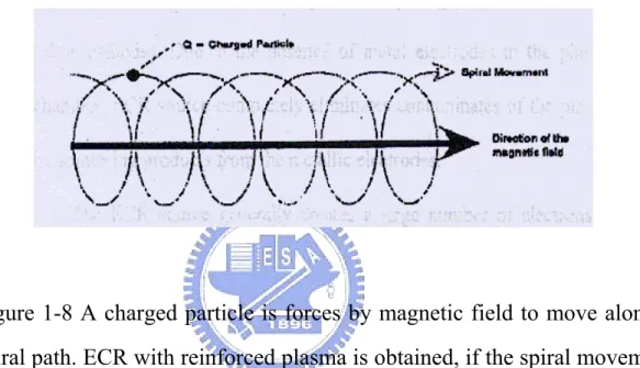
(14) Figures Caption Figure 1-1 The architecture of multilevel interconnect metallization……4. Figure 1-2 Decrease in interconnect delay and improved performance are achieved using copper and low-k dielectrics…….……….4. Figure 1-3 The cross-section of interconnect system with parasitic capacitance……………………………………………...…….5. Figure 1-4 shows the schema of polarization mechanism………………10. Figure 1-5 Frequency dependence of real part of the dielectric function……………………………………………………...10. Figure 1-6 shows high-density sources. They are (a) ECR source (b) Helicon source (c) Helical resonator and (d) Inductive source…….………………………………………………….13. Figure 1-7 The schematic illustration of the ECR microwave plasma CVD system………………………………………………..14. Figure 1-8 A charged particle is forces by magnetic field to move along a spiral path. ECR with reinforced plasma is obtained, if the spiral movement and the microwave field are synthesized....15. xii.
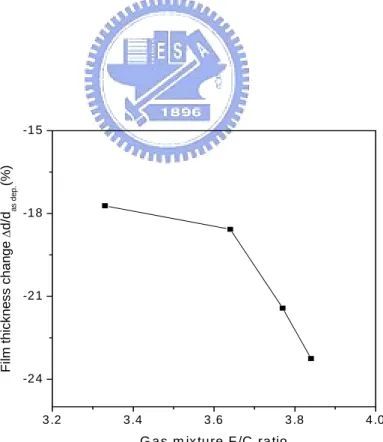
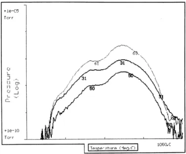
(15) Figure 2-1 Summary timeline of the materials anticipated in future generation multilevel interconnect structures………..……...19. Figure 4-1 shows the measurement methods of chemical and physical Properties……………………………………….…………...37. Figure 4-2 shows the illustration of the ECR microwave plasma CVD system………………………………………………..…….39. Figure 5-1 Optical emission spectra obtained in C2H2 and CF4 mixed gas discharge at 600W source power -200V rf bias, and 20 m Torr in the ECR-CVD…………………….……………....45. Figure 5-2 Comparisons of the plasma optical emission spectra for R = 0.97 and R = 0.90………………………………….…..….45. Figure 5-3 shows the deposition rate of a-C:F films……………………47. Figure 5-4. The Film’s thickness change after annealing as a function of flow ratio R………………………………….......................47. Figure 5-5 shows the TDA result of R = 0.90 a-C:F film. 31, 50 and 69 mean the molecule weight of CF, CF2 and CF3…………......48. Figure 5-6 shows the AFM images of R = 0.90 a-C:F films. (a) is xiii.
(16) as-deposited, and (b) is after annealed…………….………...49. Figure 5-7 shows the hardness of a-C:F films at as-deposited and after annealing…………..…………………………….……….....50. Figure 6-1 Comparing the FTIR spectrums of as-deposited a-C:F films………………………………………………………..55. Figure 6-2 FTIR spectroscopy of the a-C:F film, (a) as-deposited at R = 0.97, (b)after being annealed at R = 0.97, (c) as-deposited at R = 0.90, (d) after being annealed at R = 0.90………… ..55. Figure 6-3 Deconvoluted C 1s spectrum of a-C:F film at R = 0.97 as-deposited obtained by XPS analysis………….………...58. Figure 6-4 Fluorine concentration in the film as functions of flow ratio R…..……………………………………………………….59. Figure 6-5 C(1s) spectra change of the as-deposited a-C:F films as functions of the flow ratio R. The integrated intensities of the C(1s) spectra are normalized………………………………..60. Figure 6-6 Deconvolution result of the a-C:F film C 1s spectrum for R = 0.97 and R = 0.90 at as-deposited and after being annealed obtained by ESCA analysis…………………………….…...62. xiv.
(17) Figure 6-7 Comparisons of the HREELS spectra in the carbon K-edge region………………………………………………………..64. Figure 6-8 Carbon K-ionization edge spectra obtained from R = 0.97 as-deposited. The fit obtained when using three Gaussian peaks centered at 285, 287, and 293 eV…………………….67. Figure 6-9 shows the sp3% of as-deposited and after annealing a-C:F films………………………………………………….……...67. Figure 6-10 (a) is the R = 0.98 as-deposited HRTEM image, and (b) is after annealed one………………………………..………...69. Figure 6-11 (a) is the HRTEM image of R = 0.95 a-C:F film after annealing , and (b) is the HREELS image by carbon element mapping. of. same. film…………………………………………………………69. Figure 6-12. Dangling bond density of the a-C:F films at R = 0.97 and R = 0.90 as deposited…………………………..………......71. Figure 7-1 shows the schematic structure of MIM (Pt/a-C:F/Pt)……….76. Figure 7-2 shows the measurement methods of electronic properties…..76. Figure 7-3 Dielectric constant of the films as function of the CF4 flow xv.
(18) ratio R……………………….…………….………………..78. Figure 7-4 Leakage current of the a-C:F films of (a) R = 0.98, (b) R = 0.97, (c) R = 0.95, (d) R = 0.90…………………………….80. Figure 7-5 Electrical conductivity of the annealed films as a function of the CF4 flow ratio R………………………………………....82. Figure 7-6 sp2 bonding fraction of the annealed films as a function of the CF4 flow ratio R…………………………………….…...82. Figure 8-1 The Experiment flowchart for optical measurement………..86. Figure 8-2 PL spectra produced at R=0.97 and at R=0.90 of a-C:F films for both as-deposited and after-annealed at 300oC…….........88. Figure 8-3 shows the photoluminescence lifetime of as-deposited and 300℃ annealing a-C:F films……………………….…........89. Figure 8-4 UV/VI spectra of both R=0.97 and 0.90 of the a-C:F films as-deposited and after-annealed at 300oC……………..91. Figure 8-5 shows the energy gap of as-deposited and 300℃ annealing a-C:F films…………………………………………….…….91. xvi.
(19) Chapter 1 Overview Dielectric and optical materials have been playing an important role in the evolution of today’s electrical engineering, electronics, and information technology. The materials involved are typically crystalline, amorphous oxides, organic compounds and polymers. They are employed as bulk materials and, most often, as thin films. Dielectrics are used as insulating materials due to their property of polarization to modify the dielectric function of the vacuum, e.g. enhancing the capacity (i.e. the ability to store charges) of capacitors. They do not conduct electricity due to the very low density of free charge carriers. Here, the electrons are bound to microscopic regions within the material, i.e. the atoms, molecules, or clusters, instead of being freely movable in and out of a macroscopic system.. 1-3 General Background In the past 40 years, the electronics industry owes its phenomenal growth to the development of faster, cheaper, lighter, and smaller semiconductor products. So far the minimum scaling size has reached the maximum of transistor density. It is recognized, however, that device physics is not the first limiting factor to the continued performance improvement for systems. The challenge will be how to carry electric power and how to distribute the clock signals that control the timing and synchronize the operation. The challenge extends beyond the materials 1.
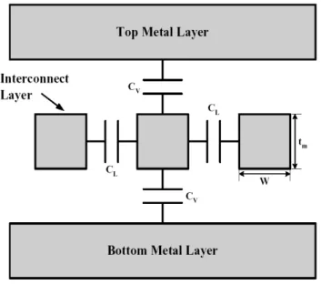
(20) properties, technologies and as well as the system architecture. On the other hand, the semiconductor industry is in progress. It accelerates the progress of Moore’s law. The dimensional scaling of back-ended interconnection (Fig. 1-1) results in the fact that not only the line-width and spaces between metal interconnections are decreased, but also the length of the interconnection lines will increase. This process will increase the RC time delay due to the higher wire resistance (R) of the narrower metal leads and the higher intra/inter-level. capacitance. (C). between. the. tightly. spaced. interconnections. While the interconnecting circuits in the cross-sectional area are reduced, the density of conducting current will rise and cause electromigration. to. worse1.. be. Furthermore,. the. length. of. the. interconnected lines will increase, owing to the larger chip size and the multilevel metallization, required for increased functional complexity and packing density of the integrated circuits. As a result, it is the characteristics of the interconnections that dominate the total circuit propagation (RC) delay, not the scaling of the active devices (Fig. 1-2)2. According to Fig. 1-3, we assume that the minimum metal pitch is equal to the twice of the metal width plus the dielectric thickness. This assumption is the same for the metal lines in between. Therefore, we consider the first-order approximation of the time delay τ and the power consumption P as follows. ⎛ L2m L2m ⎞ + 2 ⎟⎟ 2 tm ⎠ ⎝W. τ = RC = 2 ρε ⎜⎜ p = αCfV 2. (1) (2). 2.
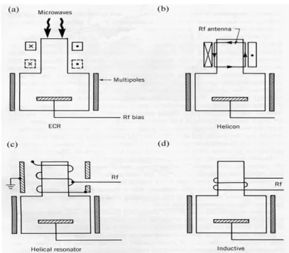
(21) , with R=ρ. Lm Wtm. (3). C = Coutput + C wire + Cinput ⎛L t LW ≈ (C L + CV ) = 2ε ⎜⎜ m m + m tm ⎝ W. ⎞ ⎟⎟ ⎠. (4). where ρ and ε are the resistivity and the permittivity, respectively. Lm, W and tm are the length of interconnected line, and thickness of the metal, respectively. α, f and V are the wire activity (i.e., when the wire is transferring a signal), frequency, and applied voltage. According to these equations, factors affecting the RC time delay can be divided into two groups: the material property (ρ and ε) and the geometric structure (Lm, W and tm). Since it is not easy to reduce the time constant by changing the geometric structure, such as the height and pitch of wire, there are two approaches to minimize the resistance × capacitance (RC) delay. One is to reduce the resistivity of the RC delay by using copper as the conductor for multi-interconnections. Copper has resistivity of 1.694 µΩ-cm which is much lower than the 2.69 µΩ-cm of aluminum. The other is to reduce the coupling capacitance between the metal lines.. This method requires low. dielectric constant (low k) materials, which can lower line to line capacitance to reduce the signal propagation delay, minimize cross-talk noise in interconnections, and alleviate power dissipation issue3, 4.. 3.
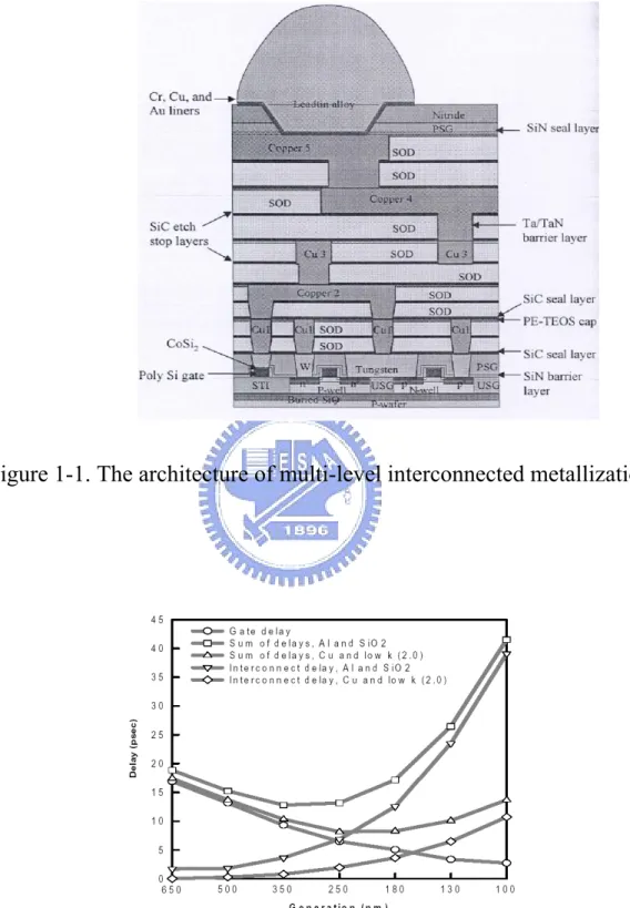
(22) Figure 1-1. The architecture of multi-level interconnected metallization.. Figure 1-2. Decrease in interconnected delay and improved performance are achieved by using copper and low-k dielectrics. (Source: Semiconductor International 2001). 4.
(23) Figure 1-3. The cross-section of interconnected system with parasitic capacitance.. 1-2 Polarization Polarization is the separation of positive and negative charge barycentres of bound charges. If this separation is induced by an applied electric field, it is called dielectric polarization. Such property of the material -- measurement of its own polarization ability -- is called the dielectric constant (or: permittivity) εr. There are several mechanisms for the dielectric polarization determined by the polarizable unit (atom, cation-anion pair, orientable permanent dipole, etc.).. 1-2-1 Electrostatic Equation with Dielectrics According to the Poisson equation, each free charge acts as a source. 5.
(24) for the dielectric displacement D: divD = ρ free. (5). where ρfree denotes the density of free (conduction) charges. Based on this relation, the overall charge neutrality of matter in an external field is described by: D = ε0E + P. (6). The term ε0E describes the vacuum contribution to the displacement D caused by an externally applied electric field E, and P represents the electrical polarization of the matter in the system. This relation is independent of the cause of the polarization. The polarization may exist spontaneously (pyroelectric polarization), it may be generated by mechanical stress (piezoelectric polarization), or, induced by an external electric field (dielectric polarization). In our case of a dielectric polarization, the polarization of the matter is related to the electric field by P = ε 0Χe E. (7). Which leads to D = ε 0 (1 + Χ e ) E = ε 0ε r E. (8). Xe : electrical susceptibility εr : relative permittivity ( or: dielectric constant). If χe or εr themselves are field-dependent, e.g. being reduced for high electric fields, tunable dielectrics are achieved.. 6.
(25) 1-2-2 Mechanisms of Polarization In general, one can distinguish between four different types of polarization5, 6: z Electronic polarization describes the displacement of the negatively charged electron shell against the positively charged nucleus. Since all matter is built from atoms, this is true for dielectrics in general. The electronic polarisability αel is approximately proportional to the volume of the electron shell. Thus, large atoms have a large electronic polarisability. Since the atomic radius is temperature-independent, generally the temperature dependence of αel can be neglected. z Ionic polarization is observed in materials with ionic bonds (i.e. ionic crystals) and described as the mutual displacement of the positive and negative sublattices under the influence of an applied electric field. In general the temperature dependence of the ionic polarisability αion is weakly positive because of the thermal expansion of the lattice. z Orientation polarization describes the alignment dipoles. In many substances there are molecules – either regular constituents or impurities – which carry a (permanent) electric dipole moment. If these dipoles are mobile or, at least able to reorient themselves by rotation, they do contribute to the dielectric polarization by the so-called orientation polarization. At ambient temperature, usually all dipole moments are mutually compensated because of the orientational disorder, i.e. the statistical distribution of their directions. An electric field, on the other hand, generates a preferred direction for the dipoles, while the thermal movement of the atoms perturbs the temperature. The solution is given by the so-called Langevin function7. For all 7.
(26) technically applied cases, the polarisability originating from permanent dipole moments p is given by α or =. p2 3k B T. (9). where kB denotes the Boltzmann constant and T the absolute temperature measured in Kevin. The strong temperature dependence is one of the main characteristics of the orientation polarization. z Space charge polarization describes a polarization effect in a dielectric material which shows spatial inhomogeneities of charge carrier densities. Space charge polarization effects are not only of importance in semiconductor field-effect devices8, they also occur in ceramics with electrically conducting grains and insulating grain boundaries9 as well as in composite material systems in which metallic particles are isolated in polymer or glass matrices. Figure 1-4 shows the schema of these four kinds of polarization mechanism. The total polarizability (i.e. αtotal = αe + αi + αo + αs ) of dielectric material results from the four contributions discussed above. The space charge only can happen in poly crystallize materials. For amorphous materials the total polarization is αtotal = αe + αi + αo. The polarization depends on the frequency of applied field. The polarizability of materials appears to decrease with increasing frequency. Each contribution stems from a short range movement of charges that respond to an electric field on. 8.
(27) different time scales and, hence, through a Fourier transform, in different frequency regimes. The dispersion of the real part of the polarizability function is shown in Figure 1-5, converting the entire frequency spectrum. At optical frequencies (1014 Hz), only the lowest species, electrons, can contribute polarization in the materials. At lower frequency, ionic polarization of induced dipoles such as a carbonyl group can occur in the infrared (1012 Hz) or lower frequency regimes. Orientation polarization is the redistribution of charge when a group of atoms with a permanent dipole align in response to the electric field. In the solid state, alignment of permanent dipoles requires considerably more time than electronic or atomic polarization, occurring at microwave (109 Hz) or lower frequencies10. The space charge polarization is caused by a drift of mobile ions or electrons which are confined to outer or inner interfaces. Depending on the local conductivity, the space charge polarization may occur over a wide frequency range from mHz up to MHz6.. 9.
(28) Figure 1-4 shows the schema of polarization mechanism.. Figure 1-5 Frequency dependence of real part of the dielectric function. 10.
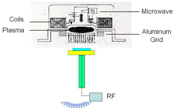
(29) 1-3 Plasma-Chemical Vapor Deposition At the end of World War II, chemical vapor deposition (CVD) expanded rapidly as researchers realized its advantages for the production of coatings and freestanding shapes. Unfortunately, with the introduction of polymer and low melting point metal films, the CVD was severely degraded by the presence of defects such as dislocations, stacking faults, vacancies, and interstitial species. These considerations often preclude the use of high (>300℃) temperatures during film formation. Furthermore, even if elevated temperatures can be tolerated, film morphology and phase structure often tied directly to deposition rate should be controlled separately. The above limitations can generally be circumvented if the energy necessary for bond cleavage is supplied by the high energy electrons in glow discharge or plasmas11, 12.. 1-3-1 High Density Plasma Source A few examples are shown schematically in Figure 1-6. They have the common features of power transfer across dielectric windows and separate bias supply at the wafer electrode. Figure 1-6 a is an electron cyclotron resonance (ECR) source. Electromagnet coils surrounding the cylindrical source chamber generate an axially varying dc magnetic field. Microwave power is injected axially through dielectric windows into the source plasma, where it excites a right-hand circularly polarized wave that propagates to a resonance zone, for cold electrons at ω = ωce, where the wave is absorbed. Here ω = 2πf is applied radian frequency and ωce = eB/m. 11.
(30) is the electron gyration frequency at resonance. For the typical microwave frequency used, f = 2450 MHz, the resonance magnetic field is B ≈ 875 G. The plasma streams out of the source into the process chamber in which the wafer is located. A helicon source is shown in Fig. 1-6 b. A weak (50-200G) dc axial magnetic field together with an rf-driven antenna placed around the dielectric cylinder that forms the source chamber allows excitation of a helicon wave within the source plasma. For the helical resonator source is shown in Fig. 1-6 c, the external helix and conducting cylinder surrounding the dielectric discharge chamber form a slow wave structure, i.e., supporting an electromagnetic wave with phase velocity much less than the velocity of light. Efficient coupling of the rf power to the plasma is achieved by excitation of a resonant axial mode. An inductive (or transformer) coupled source is shown in Fig. 1-6 d. Here the plasma acts as a single-turn conductor that is coupled to a multi-turn non-resonant rf coil across the dielectric discharge chamber; rf power is inductively coupled to the plasma by transformer action. In contrast to ECR and helicon sources, a dc magnetic field is not required for efficient power coupling in helical resonator or inductive sources13.. 12.
(31) Figure 1-6 shows high-density sources. They are (a) ECR source (b) Helicon source (c) Helical resonator and (d) Inductive source.. 1-3-2 Electron Cyclotron Resonance CVD The electron cyclotron resonance (ECR) CVD system is a high density plasma system. It can be used as CVD or dry etching functions. The ECR CVD was used to synthesize the fluorinated amorphous carbon films in the paper. Microwave power 2,45 GHz frequency is supplied to a plasma chamber through a quartz entrance window and waveguide. The magnetic field of 875 Guass for the ECR plasma excitation is generated by the coils surrounding the resonance volume and is applied perpendicularly to the surface of the substrate. A radio frequency (RF) (13.56 MHz) bias is also applied to the substrate. In order to avoid the interaction of electromagnetic fields which are between microwave and RF. The aluminum grid was used 13.
(32) to separate the electromagnetic field (Figure 1-7). The plasma stream is introduced into the deposition chamber, which is pumped down to the base pressure of 5 x 10⁻⁶ torr with a turbomolecular pump, back by a rotary mechanical pump.. Figure 1-7 The schematic illustration of the ECR microwave plasma CVD system.. ECR plasma is generated by the microwave excitation of a 2.45 GHz frequency by a magnetron through a waveguide in a resonator volume. Through the Lorentzian force acting upon the electrons, the magnetic field causes the electrons to move along circular or spiral-shaped paths, as shown in figure 1-8. The anagular frequency of the electrons is proportional to the field intensity applied by the magnets. Microwave frequency and electron movement can be synchronized by setting the 14.
(33) suitable angular frequency. This results in maximum power absorption by the electrons from the alternating electric field of the microwaves, when the collision frequency of the electrons with neutral particles is lower than the excitation frequency. This means that the ECR effect can only be used at pressures below 10-1 to 10-2 mbar.. Figure 1-8 A charged particle is forces by magnetic field to move along a spiral path. ECR with reinforced plasma is obtained, if the spiral movement and the microwave field are synthesized.. The ECR source generally creates a large number of electrons to generate a high density of plasma. Hence, the total pressure for the ECR-CVD is much less than that for PECVD (Plasma-enhanced CVD). The required power is also much lower than that for PECVD. ECR-CVD thus provides a drastic reduction in the heat load transferred from the ion source to the substrate. Consequently, the induced plasma possesses lower ion energy, and the resulting film will achieve a higher quality due to low defect density. Because of the advantages of microwave ECR-CVD method 15.
(34) such. as. lower. temperature,. large. area,. lower. ion. damage,. contamination-free and high deposition rate are good for chemical vapor deposition. Therefore we have prepared unbroken, large area, and flat fluorinated amorphous carbon films at room temperature in a short time. Moreover, the k-value can be controlled by the various flow ratios.. Reference 1 R. H. Havemann, M. K. Jain, R. S. List, A. R. Ralston, W-Y. Shih, C. Jin, M. C. Chang, E. M. Zielinski, G. A. Dixit, A. Singh, S. W. Russell, J. F. Gaynor, A. J. McKerrow, and W. W. Lee, Res. Soc. Symp. Proc., 511, 1988, p3-14. 2 L. Peters, Semiconductor International, Sep. 1998, p84. 3 M. Rossnegal and D. Mikalsen, J. Vac. Sci. Technol. A, 9, 261 (1991). 4 T. Sakurai, IEEE trans. Elec. Devices, 40, 118 (1993). 5 I. Bunget and M. Popescu, Physics of Solid Dielectrics, Elsevier, 1984, p.207. 6 R. Waser, Nanoelectronics and Information Technology, Wiley-VCH, 2003. 7 R.P. Feynman, The Feynmann Lectures on physics “Mainly Electromagnetism and Matter”, Calif. Addison-Wesley, Redwood City, 1989. 8 S.M. Sze, Physics of Semiconductor Devices, John Weily and Sons, New York, 1981. 9 R.C. Buchanan, Ceramic materials for electronics: processing, 16.
(35) properties, and applications, M. Dekker, New York, 1991. 10 J. O. Simpson and A. K. St Clair, Thin Solid Films 308, 480 (1997). 11 H.O. Pierson, Handbook of Chemical Vapor Deposition 2nd ed., Noyes, 1999. 12 M.L. Hitchman and K. F. Jensen, Chemical Vapor Deposition, Academic Press, 1993. 13 M.A. Lieberman and A. J. Lichtenberg, Principles of Plasma Discharge and Materials Processing, John Wiely & Sons, 1994.. 17.
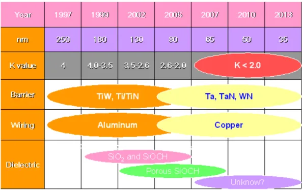
(36) Chapter 2 Literature Review 2-1 Low Dielectric Constant Materials As integrated circuit dimensions continue to shrink, interconnected RC (resistance × capacitance) delay becomes an increasingly serious problem. In order to overcome the RC time delay, incorporating new materials of low resistivity and low permittivity into interconnected structure is one solution to replace the traditional Al and SiO2. Copper is a substitute for aluminum in the future interconnection fabrication1. However, we do not know what kind of low dielectric constant (low k) material will replace the traditional SiO2 or SiOF2, 3, when a dielectric film requires a dielectric constant k < 3.0. The future low dielectric constant materials which support the semiconductor are illustrated by SIA roadmap (Fig. 2-1).. 18.
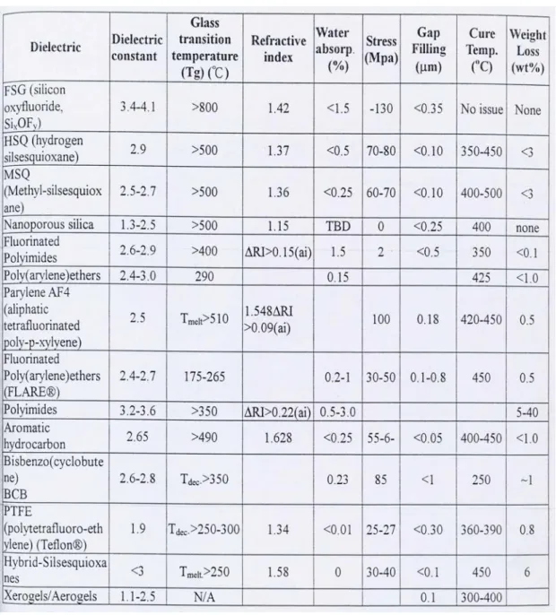
(37) Figure 2-1 summarizes the timeline of the materials anticipated in future generation multi-level interconnected structures. (Source: The International Technology Roadmap for Semiconductors: Update 2001). Table 2-1 describes the low dielectric constant materials for ULSI interconnection, and the basic requirements for low k materials are summarized in Table 2-2. The hydrogen silsesquioxane (HSQ) film and Methyl-silsesquioxane (MSQ) film which belong to SiOF base films were used in current 130 nm generation of semiconductor industry. So far maybe the k = 2.7 of black diamond film which belongs to SiOCH base film will be used in 90 nm generation of semiconductor industry. Future semiconductor devices in integrated circuits will soon be developed into a size as small as 45 nm generation, and maybe the porous SiOCH base film4 will be applied in semiconductor industry. The basic mechanical properties of the Young’s Modulus and hardness which are for semiconductor industry are about 12 GPa and 1.5 Gpa, respectively. The ultra low 19.
(38) dielectric constant materials must be lower than 2.0 for the next ULSI generation. Both porous silica (Xerogels/Aerogels) and PTFE polymer (Teflon) materials conform to the ultra low k requirement. The porous silica has high hardness and hydrophilic characteristic. These properties are disadvantageous for IC process integration of low k materials. The PTFE polymer has hydrophobic characteristic.. PTFE films can be deposited by. sputtering, but the sputtering yield is very low. The mixing of fluorocarbon and hydrocarbon gases produces fluorinated amorphous carbon (a-C:F) film by CVD methods. The a-C:F film properties are similar to PTFE. It accelerates the deposition rate and decreases the dielectric constant as well. With its lower dipole moment3 and lower electronic polarizability5 properties, the C-F bonds have a large electronegativity, therefore considered ideal to construct low dielectric material. Savage et al. were the first one to deposit a-C:F film by plasma CVD in 19756, and Endo et al. were the first one who suggested fluorinated amorphous carbon thin film as a low dielectric constant material in 19957. The permanent dipole moment of fluorinated carbon molecule is as low as 0.53, while the electronic polarizability of fluorocarbon bond is as low as 0.565. Thus, the a-C:F film is an excellent low dielectric constant material. Endo et al. used helicon plasma enhanced CVD to deposit a-C:F film8. This particular CVD brings up the deposition rate (0.15 ~ 0.3 µm/min), and accelerates the structural cross-linking in the film. Such network structure improves the thermal stability. All of the sp3 bounds of PTFE polymer are linear CF2 bonds, and the thermal stability temperature of PTFE polymer is as high as 200℃. However, some of network structure. 20.
(39) is in the a-C:F film, and its thermal stability temperature can be over 300℃. Unfortunately the highly network structure of a-C:F film will cause the dielectric constant to grow. Endo et al.9 and Yokomichi et al.10 found that nitrogen atom can help to form the cross-linking in the a-C:F:N film, of which dielectric constant is ~ 2.4 until 400℃. If we increases the fluorinate concentration in a-C:F films, we can get ultra low dielectric constant (~1.5) in a-C:F films. And then we can use hydrogen or nitrogen plasma treatment to enhance the thermal stability. In addition, a-C:F film is an ultra low k film, the a-C:F film is also an excellent field emission material11. The work function of a-C:F film is ~0.012 eV. The a-C:F film has a lot of advantages. For example, the a-C:F film has high break-down voltage, hydrophobic property, and is easy for etching.. 21.
(40) Table 2-1. Low dielectric constant materials for ULSI interconnection.. 22.
(41) Table 2-2. Basic requirements for low dielectric constant materials.. 23.
(42) 2-2 Fluorinated Amorphous Carbon Fluorocarbon film was used as a surface coating in early stage because fluorocarbon film has lower frication and hydrophobic characteristics12. Even though the fluorocarbon films are always produced after chamber cleaning or silicon dioxide etching in semiconductor industry13-16, but the fluorocarbon did not serve as low dielectric materials in integrated circuits, since the dielectric constant of silicon dioxide material was low enough for very large scale integrated (VLSI) device at that moment. However, when the semiconductor was promoted to the 180 nm ultra large scale integrate (ULSI) devices, the dielectric constant of low dielectric constant (low k) material must be lower than 3.017. Therefore, there was a demand for new interlayer insulators to improve the switching performance of ultra-large-scale integrated (ULSI) devices.. The need has led to intensive studies on several low-dielectric. materials. Among them, fluorinated amorphous-carbon (a-C:F) films have received most attention due to their thermal stability and low dielectric constant7,. 18-24. . The relationship between these properties and the film. compositions has been discussed in several studies21-25. The stability and dielectric properties could be manipulated by adjusting the F content of the films via control of the flow rate ratio of the source gases or by other techniques. A higher F concentration in the films normally reduces the thermal stability and the dielectric constant because it leads to weaker C-C cross linking, lower density and reduced polarization26-28. However, the films with high excess F, despite their thermal instability, have low leakage current and extremely high breakdown resistance. In a low. 24.
(43) temperature environment, they could be applied as excellent insulating layers. In this thesis, we report on the structural and electrical properties of the. high-F-content. a-C:F. films. prepared. by. electron. cyclotron. resonance/chemical-vapor deposition (ECR-CVD). In fluorocarbon plasma, it is well known that low F/C ratios of the precursor gases usually facilitate film growth, while high ratios induce erosion processes29. Previous studies on plasma CVD using CH4 and CF4 gases18-24 showed that the deposition rate of a-C:F films first increases with the ratio of F/C, then declines rapidly from the maxima to zero, where the ratio was calculated in consideration of the total number of F atoms divided by the total number of C atoms in the inlet gas flux per unit time. Apparently, the growth rate of a-C:F films of high F content using the source gases of very high F/C ratio was limited by the etching effect of concentrated F radicals. On the other hand, a much higher deposition rate of a-C:H films by PECVD can be achieved by using C2H2 as a precursor rather than CH430. Therefore, CF4 and C2H2 were employed as the source gases in this study to ensure a reasonable film growth rate. The microwave plasma ECR-CVD system described in this thesis was used to produce reactive chemical species, and the RF bias assisted the precursor to impinge on the substrate, resulting in the deposition of the film. Both C2H2 and CF4 were the precursors used for the synthesis of the a-C:F films. The C2H2 gas has a high C/H ratio, and could contribute enough carbon source to support a film network to increase the deposition rate31. The CF4 gas has a high F/C ratio enough to supply sufficient fluorocarbons to raise the concentration of fluorine in the a-C:F film. The CF4 plasma contains mainly CF3+ ions, F neutrals, CFn radicals and negative ion species. 25.
(44) Fluorine atoms control not only the concentration of CFn radicals through the gas-phase reactions but also the surface reactions32-36. In this thesis, we report on the chemical and physical properties of the fluorinated amorphous carbon film prepared by ECR-CVD, at CF4 flow ratios from R = 0.90 to R = 0.98, where R is CF4/[CF4+C2H2]. This is to compare the difference between the as-deposited film and the film after annealing at 300oC for 30 min. For this purpose we used the analytical instruments. as. follows:. Fourier. transform. infrared. absorption. spectrophotometer (FTIR), electron spectroscopy for chemical analyzer (ESCA), high resolution electron energy loss spectrometer (HREELS), electron. spin. resonance. spectrometer. (EPR),. photoluminescence. spectrometer (PL), ultraviolet / visible spectrophotometer (UV/VI), field emission scanning electron microscope (FESEM), pulse laser spectrometer and atomic force microscope (AFM). Current-voltage (I-V) measurements were performed with the HP4156, and the capacitance (C-V) characteristic was measured at a frequency of 1MHz using the HP4280. The sp2 content and the fluorine concentration would affect the photoluminescence lifetime, as well as energy band gap of the a-C:F films. With the rise of the temperature, the dangling bond density increases, resulting from the growing numbers of unpaired spins in the defects in the films.. 26.
(45) Reference 1 C. R. Savage, R. B. Timmons and J. W. Lin, Adv. Chem. Ser., 236, 745 (1993). 2 Kazuhiko Endo, Toru Tatsumi, J. Appl. Phys., 78, 1370 (1995). 3 CRC Handbook of Chemistry and Physics. 77th Ed., CRC Press, Boca Raton (1996). 4 A. Grill and V. Patel, J. ElCh. Soc., 151, F133 (2004). 5 K. J. Miller, J. Am. Chem. Soc., 112, 8533 (1990). 6 K. G. Budinski, J. Vac. Sic. Technol. 12, 786 (1975). 7 K. Endo, T. Tatsumi, J. Appl. Phys., 78, 1370 (1995). 8 K. Endo and T. Tatsumi, Appl. Phys. Lett., 68, 2864 (1996). 9 K. Endo and T. Tatsumi, Appl. Phys. Lett., 68, 3656 (1996). 10 H. Yokomichi, and A. Masuda, J. Non-Cryst. Solids 271, 147 (2000) 641. 11 S. H. Lai, K. P. Huang, Y. M. Pan, Y. L. Chen, L. H. Chan, P. Lin, and H. C. Shih, Chem. Phys. Let. 382, 567 (2003). 12 C. R. Savage, R. B. Timmons and J. W. Lin, Adv. Chem. Ser., 236, 745 (1993). 13 R. d’Agostino, R. Lamendola, P. Favia, and A. Giqel, J. Vac. Sci. Technol. A 12, 308 (1994). 14 G. S. Oehrlein, Y. Zhang, D. Vender, and M. Haveriag, J. Vac. Sci. Technol. A 12, 323 (1994). 15 M. J. Sowa, M. E. Littau, V. Pohray, and J. L. Cecchi, J. Vac. Sci. Technol. A 18, 2112 (2000). 16 E. A. Joseph, B. Zhou, S. P. Sant, L. J. Overzet, and M. J. Goeckner, J.. 27.
(46) Vac. Sci. Technol. A 22, 689 (2004). 17. “The. National. Technology. Roadmap. for. Semiconductors”,. Semiconductor Industry Association, San Jose, CA, 1997. 18 H. Yokomichi, T. Hayashi, T. Amano and A. Masuda: J. Non-Cryst. Solids 227, 641 (1998). 19 Y. Ma, H. Yang, J. Guo, C. Sathe, A. Agui and J. Nordgren: Appl. Phys. Lett. 72, 3353 (1998). 20 H. Yang, D. J. Tweet, Y. Ma and T. Nguyen: Appl. Phys. Lett. 73, 1541 (1998). 21 J. A. Theil: J. Vac. Sci. & Technol. B 17, 2397 (1999). 22 K. Endo and T. Tatsumi: Jpn. J. Appl. Phys. 36, L1531 (1997). 23 H. Yokomichi and A. Masuda: J. Appl. Phys. 86, 2468 (1999). 24 L. G. Jacobsohn, D. F. Franceschini, M. E. H. Maia da Costa and F. L. Freire, Jr. : J. Vac. Sci. & Technol. A 18, 2230 (2000). 25 T. W. Mountsier and J. A. Samuels: Thin Solid Films 332, 362 (1998). 26 H. Yokomichi, T. Hayashi and A. Masuda: Appl. Phys. Lett. 72, 2704 (1998). 27 K. Endo and T. Tatsumi: J. Appl. Phys. 86, 2739 (1999). 28 J. P. Chang, H. W. Krautter, W. Zhu, R. L. Opila and C. S. Pai: J. Vac. Sci. & Technol. A. 17, 2969 (1999). 29 J.W. Coburn and H. F. Winters: J. Vac. Sci. & Technol. 16, 391 (1979). 30 P.S. Andry, P.W. Pastel and W. J. Varhue: J. Mater. Res. 11, No.1. 28.
(47) (1996) 221. 31 P. S. Andry, P. W. Pastel, and W. J Varhue, J. Mater. Res. 11, 221 (1996). 32 G. Chuge and J. P. Booth, J. Appl. Phys. 85, 3952 (1999). 33 W. Schwarzenbach, G. Cunge, and J. P. Booth, J. Appl. Phys. 85, 7562 (1999). 34 K. Teii, M. Hori, M. Ito, T. Goto, and N. Ishii, J. Vac. Sci. Technol. A 18, 1 (2000) 35 L. G. Jacobsohn, D. F. Franceschini, M. E. H. Maia da Costa, and F. L. Freire, Jr, J. Vac. Sci. Technol. A 18, 2230 (2000). 36 K. Sasaki, H. Furukawa, K. Kadota, and C. Suzuki, J. Appl. Phys. 88, 5585 (2000).. 29.
(48) Chapter 3 Characterization Techniques for Fluorinated Amorphous Carbons Films. 3-1 Introduction For evaluating mechanical, electronic, chemical and physical properties of the a-C:F films, seventeen metrology tools were used to analyze them. The OES was used to detect the radicals of deposition plasma. The TDS was used to test the thermal stability of a-C:F films from 25℃ to 1050℃. The AFM and nano-indentor were used to detect the morphology and hardness of a-C:F films, respectively. The field emission scanning electron microscope (FESEM) was used to measure the thickness of a-C:F films. The composition and chemical states of the a-C:F films were analyzed by Glow Discharge Spectrometer (GDS), Fourier-Transform infrared (FTIR) Spectrometer and X-ray photoelectron spectroscopy (XPS). The microstructure was evaluated by High-Resolution Transmission Electron Microscope (HRTEM). The sp2/sp3 bond ratio was obtained through high-resolution electron energy-loss spectroscopy (HREELS, Gatan, GIF 2000). The Electron Paramagnetic resonance (EPR) equipment was used to observe the dangling bound density in a-C:F films. Current-voltage (I-V) measurements were obtained by the HP4156, and the capacitance (C-V) characteristic was measured at a frequency of 1MHz using the HP4280. The n&k Analyzer, UV-Visible Spectrophotometer 30.
(49) (UV/VI), Photoluminescence (PL), Photoluminescence (PL), and Pulse Laser were used to evaluate the optic properties of a-C:F films.. 3-2 Analyses and Measurements Techniques 3-2-1 Optical Emission Spectroscope (OES) The OES was applied to characterize the composition of the plasma. The plasma precursor is diagnosed by using OES in the visible light range (200 ~ 800 nm) and Princetron Instrument Inc. Model ST121. Optical emission in the vicinity of sample surface in the microwave discharge was collected by an optical fiber and guided into the slit (10 µm) of a 0.5-m monochrometer (Acton Research Corporation Model Spectropro-500). Spectral scans from 200 to 800 nm were recorded as synthesis conditions varied. The OES is compatibly linked to a computer, programmed to obtain qualitative information on the radicals present and their dependence on the experimental conditions.. 3-2-2 Thermal Desorption Analyze (TDA) The TDA apparatus was employed to analyze the released gas from the sample during the thermal heating. Thermal stability was tested by TDA gas analysis system (MTM Engineering, WT268) with a quadrupole mass spectrometer which characterized the released gas of fluorinated carbon bonds from 25℃ to 1050℃, and the maxima measurement range of quadrupole mass were 200 amu... 3-2-3 Atomic Force Microscope (AFM) 31.
(50) AFM uses the interaction force between the probe and surface structure feature to measure the surface topography. The AFM tip diameter of Si3N4 cantilever (Microprobes, from Digital Instruments) was measured in a scanning electron microscope around 30-40 nm. To minimize any tip-induced damages, a contact force as small as possible, a set point of -20 (ca. 25-50 nN), was employed. The scan rate was 1.5 Hz. Calibration for the in-plane length measurements was carried out with a diffraction grating whereas the height was calibrated using a series of VLSI standards. The surface topography and roughness of a-C:F films were examined by atomic force microscope (Digital instrument NS3a controller with D3100 stage).. 3-2-4 Nano-Indentor The nano-indentor (Hysitron, Hysitron 35) was used to measure hardness of the fluorinated amorphous carbon films. The Berkovich diamond tip was used to test a-C:F films’ hardness. In order to avoid the substrate effect, the thickness of a-C:F films were deposited as thick as 1.5 µm.. 3-2-5 Field-Emission Scanning Electron Microscope (FESEM) The thickness of the a-C:F films were measured by field-emission scanning electron microscope (FESEM, Hitachi S-5000, Japan) with a resolution 2nm. Comparing FESEM with α-step and n&k , the FESEM thickness data of a-C:F films are more accurate.. 3-2-6 Glow Discharge Spectrometer (GDS) The GDS apparatus has ppm level resolution. GDS (GDS750A, ECO, 32.
(51) U.S.A.) was used to characterize whether the hydrogen element exists in a-C:F films or not.. 3-2-7 Fourier-Transform Infrared Spectrometer (FTIR) FTIR is the most widely used analytic method for the molecular structure characterization of organic and inorganic compounds. The types of fluorinated carbon bonds were measured by FTIR. All samples were qualitatively analyzed by FTIR (BOMEN Model DA8.3 SNV), and the scan ranged from 500 to 4000 cm-1 with a 2cm-1 resolution. The infrared light transmitted through the sample at normal incidence and then through a KBr grating into the MCT detector. The absorption spectrums of a blanket Si is used as the background signals.. 3-2-8 X-ray Photoelectron Spectroscope (XPS) Of all the contemporary surface characterization methods, XPS is most widely used. XPS is also called electron spectroscopy for chemical analysis (ESCA). Surface analysis by XPS is accomplished by irradiating a sample with monoenergetic soft X-ray and analyzing the energy of the detected electrons. The XPS measurements were carried on Perkin Elmer model PHI 1600 by using a single Mg Kα X-ray operating at 250 W. The X-ray source is at an angle of 54.7o with respect to the analyzer. Peak energy positions were corrected by using Pt peak. Based on the result from the high-resolution spherical capacitor analyzer (SCA), the energy resolution is 1.0 eV as survey scan spectrum and 0.1 eV as core-level spectrum, respectively. We used XPS chemical shift to make the C-C, CF, CF2, and CF3 bonds certain quantities. 33.
(52) 3-2-9 High-Resolution Transmission Electron Microscope (HRTEM) HRTEM is the most powerful equipment for material microstructure analysis. The nanostructures were investigated by high-resolution transmission electron microscopy (HRTEM, JEOL, JEM-2010F and ).. 3-2-10 High-Resolution Electron Energy Loss Spectroscope (HREELS) The electronic structures of fluorinated amorphous carbon film were investigated by high-resolution energy loss spectroscope. HREELS (Gatan, GIF 2000, U.S.A.) was used to characterize sp2% in the a-C:F films. The energy resolution is 0.1 eV to characterize 1s Æ π* transition in a-C:F films.. 3-2-11 Electron Paramagnetic resonance (EPR) The dangling bonds of a-C:F films were measured by EPR. We used EPR (Bruker, EMX-10, Germany) to observe the dangling bond density from 4K to 423K. The central magnetic field is ~3400 Gauss, and the microwave is ~9.5 GHz.. 3-2-12 Capacitance-Voltage (C-V) Curve The dielectric constants of all the films were estimated according to the capacitance-voltage (C-V). The capacitance (C-V) of a-C:F films was measured at 1 MHz by HP4280 apparatus. The mask with a diameter of 250 µm was covered on a-C:F films. For the C-V measuring, the top and bottom electrodes of Pt layer were coated with the mask by the MIM structure (Pt/a-C:F/Pt). 34.
(53) 3-2-13 Current-Voltage (I-V) Curve The current-voltage characteristic of a-C:F films was observed by HP4156 at a voltage from 0 to 100V. The sample structure is MIM structure, too.. 3-2-14 n&k Analyzer The refractive index of a-C:F films were measured by n&k analyzer (n&k Technology, n&k analyzer 1200, U.S.A.), with the wavelength ranging from 190 to 1000 nm.. 3-2-15 UV-Visible Spectrophotometer (UV/VI) The optical transparence of a-C:F films was examined by HP8453 UV/VI (U.S.A.) spectrophotometer, with the wavelength ranging from 190 to 1100 nm.. 3-2-16 Photoluminescence (PL) The fluorescence was observed by a fluorescence photoluminescence (PL) apparatus with helium-cadmium (He-Cd) laser (λ= 325 nm) as an excitation source.. 3-2-17 Pulse Laser Excimer pulse laser (Lamda Physik, Mode LPX 150P,λ=193 nm) was applied to measure photoluminescence lifetime of a-C:F films. The record time unit is 10-8 second.. 35.
(54) Chapter 4 Synthesis and Characterization for Physical and Chemical Analysis. 4-1 Introduction In this work, ECR-CVD equipped with a rf bias in the chamber mixing acetylene (C2H2) and tetrafluoromethane (CF4) gases was used to prepare a-C:F film on the silicon or 7059 glass substrate. Electron cyclotron resonance chemical vapor deposition (ECR-CVD) could provide many advantages, like high density plasma, high planarity, deposition on large area, and low temperature process. Unlike SOG process, there is no moisture generated during the preparation. The acetylane (C2H2) plasma has high C/H ratio which helps to grow a-C:H film structure rapidly1,2. The tetrafluoromethane plasmas present mainly CF3+ ions, F neutrals, CFn radicals and negative species. F atoms control not only the concentrations of CFn radicals through gas-phase but also surface reactions3-7 in the plasma. In this thesis, we report on the physical and chemical properties of the fluorinated amorphous carbon film prepared by ECR-CVD at various flow ratio R, where R is [CF4]/{[CF4+C2H2]}. The relationships between the properties of the films and the mixing ratio R are as follows.. 4-2 Experiment The flowchart figure 4-2 shows the measurement methods of chemical and physical properties. 36.
(55) 3 In c h e s N -ty p e S i. S p e c im e n ts C le a n in g. E C R -C V D a -C :F. OES. A n n e a lin g 3 0 0 oC. G D S. F T I R. X P S. H R E E L S. H R T E M. F E S E M. E P R. C h e m ic a l P ro p e rtie s. T. A. D. F. A. M. P h y sic a l P ro p e rtie s. Figure 4-2 shows the measurement methods of chemical and physical Properties. 37. H A R D N E S S.
(56) 38.
(57) 4-3 Sample Preparation 4-3-1 Substrate Cleaning The n-type (100) 3-inch-diameter silicon wafers were used as the substrate material in this study. The silicon wafers were cleaned with standard RCA cleaning process in a wet bench (SCP, Santa Clara Plastics, U. S. A.). The RCA cleaning procedure has three major steps: I. Organic Cleaning: Removal of insoluble organic contaminants with a 5:1:1 H2O:H2O2:NH4OH solution. II. Oxide Strip: Removal of a thin silicon dioxide layer where metallic contaminants may accumulate as a result of (I), using a diluted 50:1 H2 O:HF solution. III. Ionic Cleaning: Removal of ionic and heavy metal atomic contaminants with a solution of 6:1:1 H2O:H2O2: HCl. The RCA cleaning technique does not attack silicon, and only a very thin layer of silicon dioxide is removed (in II) in the process. The procedure was also designed to prevent the metal contaminants from coming back to the wafer's surface. When finished, the polished side should be like speculum without any residue.. 4-3-2 Low k Film Deposition We used RF bias assisted ECR-CVD to deposit the low k a-C:F films in this study. The RF (13.56 MHz) bias was fixed at -200V, and the microwave (2.45 GHz) power was fixed at 600W. Figure 4-3 illustrates a schematic configuration of the microwave ECR microwave plasma CVD system. The C2H2 and CF4 were used as the plasma precursor. The CF4 flow rate was fixed at 100 sccm, and the C2H2 flow rate was varied from 2 39.
(58) to 10 sccm. We controlled the base pressure below 5 x 10⁻⁶ torr, and then we deposited the a-C:F films at 2 x 10⁻² torr working pressure. The temperature of the samples is the direct plasma temperature.. Figure 4-3 illustrates of the ECR microwave plasma CVD system.. Figure 4-3 shows the illustration of the ECR microwave plasma CVD system.. 40.
(59) 4-3-3 Annealing The a-C:F films were annealed at 300℃ in pure nitrogen atmosphere (Carbolite Furnace CTF 12/05/550) for 30 minutes. The velocity for increasing and decreasing temperature is +/- 3 ℃/min.. 4-4 Physical Analysis The plasma composition states were examined, using optical emission spectroscopy (OES), with the visible light range of 200-800 nm. The film thickness was measured by FESEM in the as-deposited and after annealing condition, respectively. The TDS was used to evaluate the thermal stability of a-C:F films, and the test temperature is from 25℃ to 1050℃. We monitored the gas released from thermal decomposition, and the monitoring molecular weight is from 1 amu. to 200 amu.. The film morphology was observed with a Digital Instrument NS3a Controller at a D3100 stage AFM while the hardness was measured by a Nano Scope E Hysitron 35 from Digital Instruments.. 4-5 Chemical Analysis The a-C:F films were deposited directly on Si wafers. GDS and FTIR instruments were used to examine the quality of chemical compositions and bonds. XPS, HRHEELS and EPR instruments were used to examine the quantity of compositions, electronic structures and dangling bonds of a-C:F films. HRTEM was used to observe the a-C:F film nano-structure.. 41.
(60) Reference 1 P. S. Andry, P. W. Pastel, and W. J Varhue, J. Mater. Res. 11, 221 (1996). 2 Kyu Chang Park, Jong Hyun Moon, Jin Jang, and Myung Hwan Oh, Appl. Phys. Lett., 68, 3594 (1996). 3 G. Chuge and J. P. Booth, J. Appl. Phys. 85, 3952 (1999). 4 W. Schwarzenbach, G. Cunge, and J. P. Booth, J. Appl. Phys. 85, 7562 (1999). 5 Kungen Teii, Masaru Hori, Masafumi Ito, Toshio Goto, and Nobuo Ishii, J. Vac. Sci. Technol. A 18, 1 (2000) 6 L. G. Jacobsohn, D. F. Francesschini, M. E. H. Maia da Costa, F. L. Freir, and Jr, J. Vac. Sci. Technol. A 18, 2230 (2000). 7 K. Sasaki, H. Furukawa, K. and Kadota, C. Suzuki, J. Appl. Phys. 88, 5585 (2000).. 42.
(61) Chapter 5 Physical Properties. 5-1 Introduction Fluorinated amorphous carbon (a-C:F) films were deposited by RF bias assisted microwave plasma electron cyclotron resonance chemical vapor deposition ( ECR-CVD ) with tetrafluoromethane (CF4) and acetylene (C2H2) as precursors. The deposition process was performed at flow ratios from R = 0.90 and R = 0.98, where R = CF4/( CF4+C2H2). The substrate temperature after finishing deposition was around 50oC, according to the thermal couple placed under the substrate. The thickness of as-deposited films ranged from ~ 400 Å (for R = 0.98) to ~ 700 Å (for R = 0.90). Subsequent annealing treatments of the deposited a-C:F films were carried out at 300oC for 30 min in pure nitrogen atmosphere. The higher flow ratio R led to lower deposition rate, and the hardness of a-C:F films decreased with uprising flow ratio R. The radicals of plasma were detected by OES equipment. AFM, nano-indenator and TDS were used to observe the morphology and thermal stability of a-C:F films, and FESEM was used to measure the film thickness in as-deposited condition and after annealing.. 5-2 Result and Discussion The plasma composition depends on various chemical pathways in the plasma, which again depends on the plasma parameters such as microwave power, RF power, electron temperature, electron density, gas. 42.
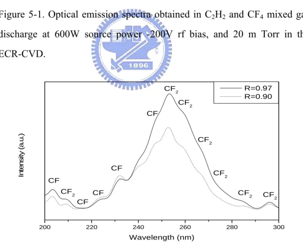
(62) flow rate, and degree of ionization. To illustrate how these collisions could result in the radical production, Table 5-1 shows a set of reactions which is the possible sheath radical production in the C2H2 and CF4 plasma1-5. The flow rate of the source gases were kept at flow ratio R (R = CF4/[(CF4+C2H2)]), 0.90, 0.95, 0.97 and 0.98. Figure 5-1 shows the optical emission spectra (OES) of the ECR excitation plasma at R = 0.90 and 0.97. There were C2, C3, CF2, CH, F2, H2 and HF radical species, and C2-, F2+ and HF+ ionic species in the plasma6. The C2 radicals will construct the main skeleton of the a-C:F films, and the fluorine atoms will be replaced by hydrocarbons to form fluorocarbon bonds or HF bonds. Figure 5-2 shows CF and CF2 species found in the plasma with the spectra for the wavelength range 200-300 nm. The F2, F2+, CF, CF2 and CF3 radicals are both sinks and sources7 at the same time during the deposition of the a-C:F films.. 43.
(63) Table 5-1. Primary electron collisions. Apparent Product Process. Potential (eV). ___________________________________________________________ e-+C2H2 Æ H++H+C2+2e20.8 H+ 22.8 Æ H++H+CH+C+2ee-+C2H2 Æ C++2H+C+2e24.5 C+ e-+C2H2 Æ CH++CH+2e22.2 CH+ e-+C2H2 Æ C2++2H +2e23.8 C2+ 18.2 Æ C2++H2 +2ee-+C2H2 Æ C2H++H +2e17.8 C2H+ e-+C2H2 Æ C2H2+ +2e11.2 C2H+ e-+C2H2+ Æ C2H +H -7.3 C2H2+ -3.2 e-+C2H2+ Æ C2 +2H -3.1 e-+C2H2+ Æ 2CH CH++C2H2 Æ C3H+ +H2 22.9 C3H+ CH++C2H2 Æ C3H2+ +H 21.3 C3H2+ C2++C2H2 Æ C4H+ +H 19.2/22.5 C4H2+ C2+H2++C2H2 Æ C4H2+ +H2 11.38 C4H2+ C2+H2++C2H2 Æ C4H3+ +H 11.07 C4H3+ CF3++CF4 Æ CF++2F 8.08 CF+ CF++CF4 Æ CF3++CF2 0.3 CF3+ 6.2 CF3++CF4 Æ CF4++CF3 Æ CF3++F+CF3 -1.78 C++CF4 Æ CF3++CF -6 e-+CF3+ Æ CF2+F -2.3 e-+CF3+ Æ CF+2F CF++CF4 Æ C++CF4+F 5.59 C+. 44.
(64) C2. Intensity (a.u.). F2. C3 CH. C2. C2. C2. -. C2. CF 2 H2. H2. HF. R =0.9. Hα. R =0.97 200. 300. 400. 500. 600. 700. 800. W avelength (nm ). Figure 5-1. Optical emission spectra obtained in C2H2 and CF4 mixed gas discharge at 600W source power -200V rf bias, and 20 m Torr in the ECR-CVD.. R=0.97 R=0.90. CF2 CF2. Intensity (a.u.). CF. CF2. CF. CF2. CF CF2. CF2. CF CF. 200. 220. 240. 260. 280. CF2. 300. Wavelength (nm). Figure 5-2 Comparisons of the plasma optical emission spectra for R = 0.97 and R = 0.90.. 45.
(65) HRSEM was used to measure the thickness of a-C:F films. The behavior of the deposition rate as a function of the flow ratio of the CF4/C2H2 gas mixture is presented in Figure 5-3. A steep decline in the deposition rate from 56 to about 3 nm/min was observed as the flow ratio increased from ~ 0.90 to ~0.98.. This indicates that the etching effect of F. radicals strengthens rapidly in the narrow region. The thermal desorption of the fragments in the a-C:F films is one of the major factors causing film shrinkage. The film thickness loss is proportional to the flow ratio R (Fig. 5-4) in a fashion similar to that of F concentration in the films, a result consistent with the lower thermal stability for the films of higher F content. Besides outgassing effect, the concurrent film structure relaxation during heat treatment may also induce shrinkage. The evolution of film microstructures, in particular, the voids observed in the films of high F content, would contribute to the change of thickness. Since the higher fluorine concentration a-C:F film has more sp3 bounds in the film, it results in thermal instability at high temperature. The TDA result of R=0.90 a-C:F film is shown in Figure 5-5. No hydrocarbon molecular signals were found in the TDA result.. There were only CF, CF2 and CF3 gases which. terminated the carbon skeleton in the films released from the film during heating process.. 46.
(66) 60. 50. nm/min. 40. 30. 20. 10. 0.88. 0.90. 0.92. 0.94. 0.96. 0.98. 1.00. R. Figure 5-3 shows the deposition rate of a-C:F films.. Film thickness change ∆d/das dep.(%). -15. -18. -21. -24. 3 .2. 3.4. 3 .6. 3.8. 4 .0. G as m ix ture F /C ratio. Figure 5-4.. The shrinkage of film thickness is negatively proportional to. flow ratio R. 47.
數據
+7
相關文件
Machine language ( = instruction set) can be viewed as a programmer- oriented abstraction of the hardware platform. The hardware platform can be viewed as a physical means
Machine language ( = instruction set) can be viewed as a programmer- oriented abstraction of the hardware platform. The hardware platform can be viewed as a physical means
External evidence, as discussed above, presents us with two main candidates for translatorship (or authorship 5 ) of the Ekottarik gama: Zhu Fonian, and Sa ghadeva. 6 In
A factorization method for reconstructing an impenetrable obstacle in a homogeneous medium (Helmholtz equation) using the spectral data of the far-field operator was developed
A factorization method for reconstructing an impenetrable obstacle in a homogeneous medium (Helmholtz equation) using the spectral data of the far- eld operator was developed
• To introduce the use of the LPF as a tool for planning the school English Language curriculum; and
Understanding and inferring information, ideas, feelings and opinions in a range of texts with some degree of complexity, using and integrating a small range of reading
Writing texts to convey information, ideas, personal experiences and opinions on familiar topics with elaboration. Writing texts to convey information, ideas, personal
(a) The principal of a school shall nominate such number of teachers of the school for registration as teacher manager or alternate teacher manager of the school as may be provided
