直接降頻雙頻帶接收器前端電路
81
0
0
全文
(2)
(3) Direct Conversion Dual-Band Receiver Front-End Circuit. Student. Ching-Ming Fu. Advisor Chien-Nan Kuo. A Thesis Submitted to Department of Electronics Engineering & Institute of Electronics College of Electrical Engineering and Computer Science National Chiao Tung University In Partial Fulfillment of the Requirements For the Degree of Master of Science In Electronic Engineering June 2004 Hsinchu, Taiwan, Republic of China.
(4)
(5) Direct Conversion Dual-Band Receiver Front-End Circuit Student: Ching-Ming Fu. Advisor: Prof. Chien-Nan Kuo. Department of Electronics Engineering & Institute of Electronics National Chiao-Tung University. ABSTRACT The aim in this thesis is mainly based on the design of front-end circuit in the receiver of wireless LAN systems using standard 0.18um CMOS process. Also, a concurrent dual-band LNA is designed first for wireless LAN applications. The low noise amplifier and the front-end circuit were verified through two individual chips. In the first chip, a concurrent dual-band step-gain low noise amplifier is analyzed and designed for wireless local area network (WLAN) operating at both 2.4 and 5.5-GHz bands. We employ the LC tank with L-degeneration in series to achieve dual-band input impedance matching design. Measured data show that the amplifier achieves maximum power gains (S21s) of 11 and 8.5 dB at 2.45 and 5.5-GHz, respectively. The input return losses (S11s) are about -10dB at both bands, and the noise figures are 4 and 5.4dB at the 2.45 and 5.5-GHz bands while consuming 14.6mW. In the second chip, a dual-band front-end circuit, intended for use in the receiver. i.
(6) path of the wireless LAN systems, is analyzed and designed. We revise the techniques of gain control to achieve better performance, and add additional CMOS pair mixer with high-pass load to down convert signal. The simulated data show that the amplifier achieves maximum power gain (S21) of 25 dB, input return loss (S11) better than -10 dB, and average noise figure of 7dB at both bands, while consuming only 21mW.. ii.
(7) :. :. 0.18um CMOS. (L-degeneration) 2.45 (S21) 11.5. 8dB. 3.5dB. (S11) 11mW. CMOS (S21) 25dB 7dB. (S11) 21mW. iii. -10 dB. 5.5GHz -10dB.
(8) iv.
(9) CONTENTS ABSTRCT (ENGLISH)................................................. i ABSTRCT (CHINESE)............................................... iii ACKNOWLEDGEMENT........................................... iv CONTENTS .................................................................. v TABLE CAPTIONS .................................................. viii FIGURE CAPTIONS .................................................. ix Chapter 1. INTRODUCTION ................................... 1. 1.1 Motivation .................................................................... 1 1.2 Thesis Organization..................................................... 2. Chapter 2. FRONT-END CIRCUIT. BACKGROUND........................................................... 4 2.1 Receiver Architecture .................................................. 4 2.2 Wireless Local Area Network...................................... 5 2.2.1. IEEE 802.11a.......................................................................5. 2.2.2. IEEE 802.11b.......................................................................6. 2.3 Noise Basic.................................................................... 8 2.3.1. Noise Source........................................................................9. 2.3.2. Noise Model of MOSFET..................................................10. 2.3.3. Noise Figure of Cascaded Stages .......................................13 v.
(10) 2.4 Linearity Basic ........................................................... 13 2.4.1. Harmonics..........................................................................14. 2.4.2. Gain Compression..............................................................14. 2.4.3. Inter-Modulation................................................................14. 2.4.4. Linearity of Cascaded Stages .............................................16. 2.5 LNA Basic................................................................... 16 2.5.1. Input Impedance Matching ................................................17. 2.5.2. Noise Analysis ...................................................................18. 2.6 Down-Conversion Mixer Basic ................................. 21 2.6.1. Conversion Gain ................................................................22. 2.6.2. SSB and DSB Noise Figures..............................................22. 2.6.3. Port-to-Port Isolation .........................................................23. 2.6.4. Single-Balanced and Double-Balanced Gilbert Mixer........23. Chapter 3. Concurrent Dual-Band LNA ................ 26. 3.1 Introduction ............................................................... 26 3.2 Principle of the Circuit Design.................................. 27 3.2.1. Dual-Band Input Matching ................................................28. 3.2.2. Dual-Band Gain Analysis...................................................29. 3.2.3. Noise Analysis ...................................................................30. 3.2.4. Dual-Band Output Matching..............................................31. 3.2.5. Step Gain Function ............................................................32. 3.3 Chip Implementation and Measured Result ............ 34 3.3.1. Microphotograph of Chip...................................................34. 3.3.2. Measurement and Simulation Result..................................35. Chapter 4. Dual-Band Front-End Circuit .............. 43. 4.1 Introduction ............................................................... 43 4.2 Principle of the Circuit Design.................................. 44 vi.
(11) 4.2.1. Concurrent Dual-Band LNA ..............................................44. 4.2.2. Variable Gain Stage............................................................46. 4.2.3. CMOS Pair Mixer..............................................................47. 4.2.4. High-Pass Load..................................................................48. 4.3 Chip Implementation and Measured Result ............ 51 4.3.1. Microphotograph of Chip...................................................51. 4.3.2. Measurement and Simulation Result..................................51. Chapter 5. SUMMARY AND FUTURE WORK.... 61. 5.1 Summary .................................................................... 61 5.2 Future Work............................................................... 62. REFERENCES ........................................................... 63 VITA ............................................................................ 65. vii.
(12) TABLE CAPTIONS TABLE.I.. Summary of simulation and measured result of concurrent dual-band LNA ............................................................................................. 42. TABLE.II.. Comparison of dual-band front-end circuit and previously publish work............................................................................................. 53. viii.
(13) FIGURE CAPTIONS Fig.2.1. 802.11a Channel Distribution..................................................................... 6. Fig.2.2. 802.11b Channel Distribution..................................................................... 7. Fig.2.3. (a) MOSFET Noise Model (b) Equivalent Input Referred Noise Model.... 12. Fig.2.4. (a) Input Stage of the L-Degeneration Cascode LNA (b) Equivalent Model.. ................................................................................................................ 17. Fig.2.5. Noise Model of the Cascode LNA with L-Degeneration........................... 19. Fig.2.6. (a) Single-Balanced Gilbert Mixer (b) Double-Balanced Gilbert Mixer .... 24. Fig.3.1. Schematic of the Concurrent Dual-Band LNA with 3 Step Gain............... 27. Fig.3.2. (a) The Input Stage of the Concurrent Dual-Band LNA (b) Equivalent Model 28. Fig.3.3. Equivalent Noise Model of the Concurrent Dual-Band LNA Input Stage.. 30. Fig.3.4. Output Matching Network of the Concurrent Dual-Band LNA................. 31. Fig.3.5. Resistor-Chain Gain Control Technique ................................................... 33. Fig.3.6. Microphotograph of Concurrent Dual-Band LNA with 3 Step Gain Circuit .. ................................................................................................................ 34. Fig.3.7. The Equivalent Model with path and Cgd .................................................. 36. Fig.3.8. The Effect of the Path Inductor................................................................. 36. Fig.3.9. S11 of Concurrent Dual-Band LNA at High Gain Mode........................... 38. Fig.3.10. S22 of Concurrent Dual-Band LNA at High Gain Mode....................... 38. Fig.3.11. S21 of Concurrent Dual-Band LNA at High Gain Mode....................... 39. Fig.3.12. S12 of Concurrent Dual-Band LNA at High Gain Mode....................... 39 ix.
(14) Fig.3.13. Noise Figure of Concurrent Dual-Band LNA at High Gain Mode......... 40. Fig.3.14. Linearity at 2.45GHz............................................................................ 40. Fig.3.15. Linearity at 5.5GHz.............................................................................. 41. Fig.3.16. 3 Step Gain Function............................................................................ 41. Fig.3.17. Noise Figure in 3 different Gain Modes................................................ 42. Fig.4.1. Schematic of the DCR Dual-Band Front-End Circuit with Variable Gain . 44. Fig.4.2. Modified Concurrent Dual-Band LNA ..................................................... 45. Fig.4.3. Variable Gain Stage.................................................................................. 46. Fig.4.4. CMOS Pair Mixer .................................................................................... 47. Fig.4.5. Single Transistor and the CMOS pair ....................................................... 48. Fig.4.6. High-Pass Load........................................................................................ 49. Fig.4.7. (a) Basic High-Pass Load (b) Equivalent Model....................................... 50. Fig.4.8. Miller Capacitor Amplifier ....................................................................... 50. Fig.4.9. Microphotograph of Dual-Band Front-End............................................... 51. Fig.4.10. PCB layout of (a) Front-End Circuit (b) Unit Gain Output Buffer......... 54. Fig.4.11. Input Return Loss of Dual-Band Front-End Circuit .............................. 55. Fig.4.12. Simulation Results of Conversion Gain (a) 2.45GHz (b) 5.5GHz ......... 56. Fig.4.13. Measured Results of Conversion Gain at 2.6GHz ................................. 57. Fig.4.14. Simulation Results of Noise Figure (a) 2.45GHz (b) 5.5GHz................ 58. Fig.4.15. Simulation Results of Linearity (a) 2.45GHz (b) 5.5GHz...................... 59. Fig.4.16. Measured Results of IIP3 at 2.6GHz..................................................... 60. x.
(15) Fig.4.17. Measured Results of IIP2 at 2.6GHz..................................................... 60. xi.
(16)
(17) Chapter 1. 1. Chapter 1 INTRODUCTION 1.1 Motivation Wireless communications at multi-gigahertz frequency are predicted to play a critical role in recent days. The radio-frequency (RF) transceivers are increasingly taking advantage of technology advances in CMOS that make the integration of complete communications systems and low cost possible. Standard receiver architectures, such as super-heterodyne and direct conversion, all include the stages of low noise amplifier (LNA) and mixer. The low noise amplifier (LNA) provides high gain and low noise to suppress the overall system’s noise performance. On the other hand, the mixer down converts the radio-frequency (RF) signal to base-band directly or through intermediate frequency (IF) by twice and needs high linearity to avoid some problems, such as harmonic generation, gain compression, desensitization, blocking, cross modulation and inter-modulation, etc. . There are multiple standards in the wireless local area network (LAN), such as 802.11a/b/g, which operate at 2.4-2.5 and 5.2-5.8-GHz. Therefore, the dual-band radio frequency (RF) front-end circuit is needed for the integration of the wireless LAN. How to provide suitable front-end circuit for specific wireless communication system is the main object of this thesis. Two low noise amplifiers (LNA) and one front-end circuit for wireless LAN are analyzed, designed and implemented. In the first one for wireless LAN dual-band application, dual-band impedance matching and dual-band gain are designed at 2.4 to 2.5-GHz.and 5.2 to 5.8-GHz for wireless LAN application. A step gain function is also added to enhance the dynamic range of the input signal In the second one for wireless LAN 802.11b application, popular cascode stage is.
(18) Chapter 1. 2. replaced by a common source stage for low power consumption. The supply voltage can be decreased a half of the original cascode stage. The problem of isolation is solved by a transformer to cancel the reverse signal. In the last one for wireless LAN dual-band application, a dual-band front-end circuit for direct conversion receiver (DCR) is designed. In the same, a variable gain function to enhance the dynamic range of the input signal is added. Besides, A high-pass mixer load is designed and added for the DC-offset cancellation.. 1.2 Thesis Organization In this thesis, the circuits for wireless LAN application are presented. Many functions of low noise amplifier (LNA) and front-end circuits are designed to satisfy the application of wireless LAN application. By these circuits, the radio frequency (RF) signals can be enlarged and down convert to the base-band. In Chapter2, some front-end basics are introduced. These basics provide a guidance to design a front-end. There are some basic concepts of WLAN standard, noise, linearity, LNA and mixer blocks included in this chapter. In Chapter 3, a dual-band LNA with 3 step gain for 2.4 and 5-GHz wireless LAN application is introduced. The detailed circuit analysis and design equation is presented. Circuit simulation and comparison with single band LNA are also discussed. Finally, measurement result of the LNA chip fabricated by TSMC 0.18 m CMOS technology is discussed and compared to some single band LNA, In Chapter 4, a DCR dual-band front-end circuit is discussed. The first stage is the concurrent dual-band LNA which is the same as that in Chapter 1. But the technique of variable gain function to enhance dynamic range is replaced. Also, the impedance matching is advised for better performance. In the second stage, traditional.
(19) Chapter 1. 3. Gilbert mixer is replaced by CMOS pair mixer for higher linearity. On the other hand, a high-pass load for easing DC-offset is designed and introduced. Overall front-end circuit is implemented. In the last chapter, the work is summarized and concluded. Also, there is some future work..
(20) Chapter 2. 4. Chapter 2 FRONT-END CIRCUIT BACKGROUND This chapter presents an overview of the receiver front-end architecture and key concepts. The receiver front-end amplifies the input signal from antenna and down convert the signal into base-band. These basic concepts provide a guidance to design a front-end for suitable system. The problems of noise and nonlinearity and the mainly block of receiver, such as LNA and mixer, are also introduced and discussed.. 2.1 Receiver Architecture There are many kinds of receiver architectures, such as heterodyne receivers and homodyne receivers. Each of them takes its own advantages and disadvantages. Low IF receiver architectures and direct conversion receiver (DCR) architectures have gained much interest recently. Low IF receiver architectures avoid the use of expensive (discrete) components such as image-reject (IR) filters, allowing a higher level of integration. The problems of Dc-offset and local-oscillator (LO) self-mixing in low-IF receivers are not so severe compared to those in zero-IF receivers. On the other hand, low-IF receivers do have image problems. Among different architectures of receivers, the direct conversion architecture, also known as the homodyne, is attractive when low cost and power consumption are at a premium. There are a mixer which down converts the desired channel to zero IF and a filter which removes adjacent channels at base-band in DCR architecture. If the.
(21) Chapter2. 5. IF is not at dc, an IR filter or other arrangement is required to suppress the image channel. This inevitably consumes substantial cost and power. Furthermore, an active low-pass channel select filter at zero IF always obtains a given dynamic range with lower power than a band-pass filter with the same pass-band centered at some nonzero IF. Also, RF receivers should provide variable gain and multi-band operation in the near future to increase the functionality. The function of variable gain enhances the dynamic range of input signal. Covering multi-band operation can lower the cost and power.. 2.2 Wireless Local Area Network Wireless LANs (WLANs) provide wideband wireless connectivity between PCs and other consumer electronic devices. Beside, WLANs allow accessing to core network and other equipment in corporate, public, and home environments.. 2.2.1 IEEE 802.11a The IEEE 802.11a standard, which refers to the 5 GHz, was defined in 1999. The lower and middle U-NII sub-bands accommodate eight channels in a total bandwidth of 200 MHz and the upper U-NII band accommodates four channels in a 100 MHz bandwidth. The centers of the outermost channels shall be at a distance of 30 MHz from the band' s edges for the lower and middle U-NII bands, and 20 MHz for the upper U-NII band, which is shown in Fig.2.1. The physical layer of 802.11a is based on a 52 carrier orthogonal frequency division multiplexing (OFDM) modulation scheme..
(22) Chapter 2. 6. Theoretically, the maximum data rate can be achieved up to 54 Mb/s with 64 quadrature amplitude modulation (64-QAM). The cost of increasing the spectral efficiency according to the 802.11a standard is a strict requirement on the signal-to-noise ratio (SNR). A higher SNR results in more stringent demands on noise performance and image rejection. The specification of the IEEE 802.11a standard recommends a noise figure of 10 dB, with a 5 dB implementation margin, to accommodate the worst-case situation.. Fig.2.1. 802.11a Channel Distribution. 2.2.2 IEEE 802.11b The IEEE 802.11b standard operating at 2.4 GHz was also defined in 1999..
(23) Chapter2. 7. There are maximum fourteen channels in a 100 MHz bandwidth, and the centers of the outermost channels shall be at a distance of 10 MHz from the band' s edges as shown in Fig.2.2.. Fig.2.2. 802.11b Channel Distribution. The basic access rate shall be based on 1 Mb/s DBPSK modulation and the enhanced access rate shall be based on 2 Mb/s DQPSK modulation. The extended direct sequence specification defines two additional data rates. The High Rate access rates shall be based on the CCK modulation scheme for 5.5 Mb/s and 11 Mb/s. An optional PBCC mode is also provided for potentially enhanced performance. About receiver minimum input level sensitivity, the frame error ratio (FER) shall be.
(24) Chapter 2. 8. less than 8 × 10 −2 at a PSDU length of 1024 octets for an input level of –76 dBm measured at the antenna connector. This FER shall be specified for 11 Mb/s CCK modulation. The test for the minimum input level sensitivity shall be conducted with the energy detection threshold set less than or equal to –76 dBm. The sum of the noise figure (NF) and the signal-to-noise ratio (SNR) is about 24.6 dB. Assuming SNR is 10dB for the required FER and 2 dB of IL, arriving at a noise figure of 12.6 for the receiver.. 2.3 Noise Basic Noise can be loosely defined as any random interference unrelated to the signal of interest. The noise limits the sensitivity of communication systems. In analog circuits, the signal-to-noise ratio (SNR), defined as the ratio of the signal power to the total noise power, is an important parameter. In RF design, on the other hand, even though the ultimate goal is to maximize the SNR for the received and detected signal, most of the front-end receiver blocks are characterized in terms of their “noise figure” rather than the input-referred noise. Noise figure can be expressed as Noise Figure = 10 log 10 ( noise. factor ) = 10 log 10 (. SNRin ) SNRout. (2-1). where SNRin and SNRout are the signal-to-noise ratios measured at the input and output, respectively. Noise figure is a measure of how much the SNR degrades as the signal passes through a system. If a system has no noise, then SNRout= SNRin, regardless of the gain. Therefore, the noise figure of a noiseless system is equal to unity. In reality, the finite noise of a system degrades the SNR, yielding NF > 1..
(25) Chapter2. 9. 2.3.1 Noise Source There are many kinds of noise source, such as thermal noise, shot noise, and flicker noise 0. Thermal noise is generated by resistors. In conventional resistors, it is due to the random thermal motion of the electrons and is unaffected by the presence or absence of direct current. Since typical electrons drift velocities in a conductor are much less then electron thermal velocities. Thermal noise is directly proportional to absolute temperature T. In a resistor R, thermal noise can be shown to be represented by a series voltage generator v 2 = 4 kTR∆f or by a shunt current generator i 2 = 4kT∆f R , where k is Boltzmann’s constant and ∆f is the bandwidth in hertz. Shot noise is always associated with a direct current flow and is present in diodes, MOS transistors, and bipolar transistors. The origin of shot noise can be seen by considering the diode and the carrier concentrations in the device in the forward-bias region. The passage of each carrier across the junction, which can be modeled as a random event, is dependent on the carrier with sufficient energy and a velocity directed toward the junction. Shot noise is a Gaussian white process associated with the transfer of charges across an energy barrier (e.g., a p-n junction). The effect of shot noise can be represented in the low frequency, small-signal equivalent circuit of the diode by inclusion of a current generator shunting the diode. If a current I is composed of a series of random independent pulses with average value ID, then the resulting noise current generator has a mean square value i 2 = 2 qI D ∆f ,. where q is the electronic charge and ∆f is the bandwidth in hertz. Flicker noise is a type of noise found in all active devices, as well as in some discrete passive elements such as carbon resistors. The origins of flicker noise are.
(26) 10. Chapter 2. varied, but it is caused mainly by traps associated with contamination and crystal defects. These traps capture and release carriers in a random fashion and the time constants associated with the process give rise to a noise signal with energy concentrated at low frequency. Flicker noise, which is always associated with a flow of direct current, displays a spectral density of the form i 2 = K 1 I a ∆f f b , where K1 is a process-dependant. constant, a is a constant in the range of 0.5 to 2, b is a constant of about unity and ∆f is the bandwidth in hertz.. 2.3.2 Noise Model of MOSFET The noise source of MOSFET can be categorized into drain noise and gate noise, mainly [2]. The dominate noise source in a MOSFET is the channel noise, which basically is a thermal noise originated from the voltage-controlled resistor mechanism of a MOSFET. Another source of drain noise is flicker noise. Because MOS transistors conduct current near the surface of the silicon where surface states act as traps that capture and release current carriers, their flicker noise component can be large. Therefore, the mean-square drain noise of MOSFET can be present as a shunt noise current generator. id2 = 4kTγg d 0 ∆f + where. K1 ω t A∆f f. (2-1). is a bias dependence factor, gd0 is the zero-bias drain conductance of the. device, K1 is a process-dependant constant, A is area of gate, frequency of MOSFET and ∆f is the bandwidth in hertz.. t. is the cutoff.
(27) Chapter2. 11. Another source of noise in the MOS transistor is shot noise generated by the gate leakage current. This is very small since the dc gate current IG is typically less than 10 -15 A. The noise term is all independent with i d2 .. On the other hand, there is one other component of noise that is usually insignificant at low frequencies but important in radio frequency. If the MOS transistor is biased so that channel operates in the inverted condition, fluctuations in channel charge will induce ac gate current due to the coupling of the capacitance between the gate and channel. The gate noise current is correlated with the thermal noise term of i d2 because both noise currents stem from thermal fluctuations in the channel. The magnitude of the correlation between gate and drain thermal noise can be expressed mathematically as. i g ⋅ i d*. c≡. i g2 ⋅ id2. = 0.395 j. (2-3). where the value of 0.395j is exact for long channel devices. The total mean-square gate noise in the sum of above two terms can be present as a shunt noise current generator. i g2 = 4kTδg g ∆f + 2qI G ∆f. (2-4). where is a constant which is equal to 3/4 in long channel device while 4 to 6 in short channel one and the parameter gg gg =. ω 2 C gs2. (2-5). 5g d 0. Because there is a correlation between gate and drain thermal noise, the gate noise can be re-expressed as 2. 2. 2 2 i g2 = 4kTδg g c ∆f + 4kTδg g (1 − c )∆f + 2qI G ∆f = i gc + i gu. (2-6).
(28) Chapter 2. 12. where the first term is correlated to drain noise and other terms is uncorrelated. Because of the correlation, special attention must be paid to the reference polarity of the correlated component. The value of correlation coefficient c is positive for the polarity. From previous introduction of MOS transistor noise source, a standard MOSFET noise model can be presented in Fig.2.3. (a). (b). Fig.2.3. (a) MOSFET Noise Model (b) Equivalent Input Referred Noise Model. 2 2 are the correlated and and i gu In Fig.2.3 (a), i d2 is the drain noise current, i gc. uncorrelated terms of the gate noise current and v rg2 is thermal noise of gate parasitic. resistor. The noise model can be represented as a noiseless network and two equal noise 2 and i eq2 in Fig.2.3 (b). The shot noise is too small to be neglected and sources v eq. the flicker noise can also be neglected for operating at Giga hertz. Therefore, the input referred noise sources can be expressed as.
(29) Chapter2. 2 v eq = v rg2 + i g2 ⋅ rg2 +. i d2 ⋅ (1 + ω 2 C gs2 rg2 ) g m2. = 4 kT∆f ( rg + δg r + 2 g g. i =i +i 2 eq. 2 gc. 2 gu. γg d 0 g m2. 13. (2-7). ⋅ (1 + ω C r )) 2. 2 2 gs g. i d2 γg + 2 ⋅ ω 2 C gs2 = 4 kT∆f (δg g + d2 0 ⋅ ω 2 C gs2 ) gm gm. (2-8). 2.3.3 Noise Figure of Cascaded Stages For a cascade of stages, the overall noise figure can be obtained in terms of the NF and gain of each stage [3]. For m stages, the overall noise figure of cascaded stages can be expressed as. NFtot = 1 + ( NF1 − 1) +. NF2 − 1 + A p1. +. NFm − 1 A p1 A p ( m −1). (2-9). where the NF of each stage is calculated with respect to the source impedance driving that stage. This is called the Friis equation. The Friis equation indicated that the noise contributed by each stage decreases as the gain preceding the stage increases, implying that the first few stages in a cascade are the most critical. Conversely, If a stage exhibits attenuation (loss), then the noise figure of the following circuit is amplified when referred to the input of that stage.. 2.4 Linearity Basic A system is linear if its output can be expressed as a linear combination of responses to individual inputs. In this section we discuss the important of linearity in the RF system, and introduce the effects caused by nonlinearity. For simplicity, we limit our analysis to memory-less, time-variant systems and assumed.
(30) Chapter 2. 14. y ( t ) ≈ a 1 x (t ) + a 2 x 2 ( t ) + a 3 x 3 ( t ). (2-10). 2.4.1 Harmonics If a sinusoid is applied to a nonlinear system, the output generally exhibits frequency components that are integer multiples of the input frequency. In Eq. (2-10), If x(t)=Acos( t), then. y (t ) = a1 A cos(ωt ) + a 2 A 2 cos 2 (ωt ) + a 3 A 3 cos 3 (ωt ) =. a A3 3a A 3 a 2 A2 a A2 + ( a1 A + 3 ) cos(ωt ) + 2 cos(2ωt ) + 3 cos(3ωt ) 2 4 2 4. (2-11). where the term with the input frequency is called the fundamental and the higher order terms the harmonics.. 2.4.2 Gain Compression The small-signal gain of a circuit is usually obtained with the assumption that harmonics are negligible. However, as the input signal amplitude increase, the gain begins to vary. In Eq. (2-11), gain is equal to the coefficient term of the fundamental. In most circuits of interesting, the output is a compressive or saturating function of the input, and the gain approached zero for sufficiently high input. In Eq. (2-11), this occurs if a 3<0. And the gain is a decreasing function of A. In RF circuits, this effect is quantified by the 1-dB compression point, defined as the input signal level that causes the small-signal gain to drop by 1dB.. 2.4.3 Inter-Modulation When two signals with different frequencies are applied to a nonlinear system,.
(31) Chapter2. 15. the output in general exhibits some components that are not harmonics of the input frequencies. Called inter-modulation (IM), this phenomenon arises from mixing of two signals when their sum is raised to a power greater than unity. If the input signal is x(t)=A1cos(. 1t)+A2cos(. 2t),. Then the output signal can be expressed as. y (t ) = a1 ( A1 cos(ω1t ) + A2 cos(ω 2 t )) + a 2 ( A1 cos(ω1 t ) + A2 cos(ω 2 t )) 2 + a 3 ( A1 cos(ω1t ) + A2 cos(ω 2 t )) 3. (2-12). The inter-modulation products can be obtained by expanding the left side of Eq. (2-12). The third-order IM products at 2. IM 3 =. 1-. 2. and 2. 2-. 1. is presented as. 3a 3 A12 A2 3a A 2 A cos(2ω1 − ω 2 )t + 3 2 1 cos( 2ω 2 − ω1 )t 4 4. (2-13). and the fundamental components can be expressed as. 3 3 a 3 A13 + a 3 A1 A22 ) cos(ω1t ) 4 2 3 3 + ( a1 A2 + a 3 A23 + a 3 A2 A12 ) cos(ω 2 t ) 4 2. fundamental = (a1 A1 +. The key point here is that if the difference between 2. 1-. 2. and 2. 2-. 1. appear in the vicinity of. 1. and. (2-14). 1 2,. and. 2. is small, the IM3 at. thus revealing nonlinearities.. The corruption of signal due to third-order inter-modulation of two nearby interferers is so common and so critical that performance metric has been defined to characterize this behavior. Called the third intercept point (IP3). This parameter is measured by a two-tone test in which A is chosen to be sufficiently small so that higher-order nonlinear terms are negligible and the gain is relatively constant and equal to a1. When IM3 equals to the fundamental as input signal level increases, the input signal level is called the input IP3 (IIP3) and the output signal level is called the output IP3 (OIP3). We can derive the input IP3 from Eq. (2-13) and Eq. (2-14).
(32) Chapter 2. AIP 3 =. 16. 4 a1 3 a3. (2-15). and the output IP3 is equal to a 1AIP3.. 2.4.4 Linearity of Cascaded Stages Since in RF systems, signals are processed by cascaded stages, it is important to know how the nonlinearity of each stage is referred to the input of the cascade. In particular, it is desirable to calculate an overall input third intercept point in terms of the IP3 and gain of the individual stages. For three or more stages, there is the following general expression a12 a 12 b12 1 1 ≈ + + + 2 2 AIP2 3 AIP AIP AIP2 3,3 3,1 3, 2. (2-16). where AIP3 is the IIP3 of overall system, AIP3,m is the IIP3 of the mth stage, a 1 and b1 are the coefficients of each stage. If each stage in a cascade has a gain greater than unity, the nonlinearity of the last few stages are more important because the IP3 of each stage is effectively scaled down by the total gain preceding that stage. By the way, the Eq. (2-16) is merely an approximation, more precise calculations or simulations must be performed to predict the overall IP3.. 2.5 LNA Basic LNA, whose main function is to provide enough gain and to overcome the noise of subsequent states and produce low noise, is typically the first stage of RF front-end circuit. An LNA should accommodate large signal without distortion and frequently.
(33) Chapter2. must also present at specific impedance, such as 50. 17. , to the input source while. adding as little noise as possible. There are several common goals in the design of low noise amplifier, which include minimizing the noise figure of the amplifier, providing enough gain with sufficient linearity and providing a stable 50. input impedance to terminate an. unknown length of transmission line which delivers signal from the antenna to the amplifier in the frequencies of interesting. A good input match is even more critical when a pre-select filter precedes the LNA because such filters are often sensitive to the quality of their terminating impedances. The additional constraint of low power consumption and multi-band which is imposed in portable and multi-standard systems further complicates the design process.. 2.5.1 Input Impedance Matching The first work of designing a LNA is to provide stable input impedances. The most popular method in recent days is L-degeneration, which is suggested by Thomas H. Lee and Derek K. Shaeffer in 1997 [4].. (a). Fig.2.4. (b). (a) Input Stage of the L-Degeneration Cascode LNA (b) Equivalent Model.
(34) Chapter 2. 18. The circuit of Fig.2.4 (a) is the input stage of the cascode LNA using L-degeneration. Selecting the first stage of a LNA is a very important thing for obtaining good both noise and input matching. The input Impedance of the LNA can be derived from the equivalent small signal model of Fig.2.4 (b). Z in =. gm 1 L S + s( LS + L g + 2 ) = ω t LS C gs s C gs. (ω = ω 0 =. 1 ( LS + L g )C gs. ). (2-17). where we obtain the input impedance Zin is equal to the multiplication of cutoff frequency of the device and source inductance at resonant frequency, this value will be set to 50. for input matching in the RF design. Therefore, the source inductance. Ls is chosen to provide the desired input resistance. Since the input impedance is pure resistive only at resonance, an additional degree of freedom, provided by the gate inductor Lg, is needed to guarantee this condition. The common-gate transistor of the cascode LNA, M2, plays two important roles by increasing the reverse isolation of the LNA. First, it lowers the LO leakage produced by the following mixer. Second, it improves the stability of the circuit by minimizing the feedback from the output to the input. The benefits of cascade LNA still include current reuse and Miller effect degradation.. 2.5.2 Noise Analysis Fig.2.5 is the noise model of the cascode LNA with L-degeneration. The resistor rg represents the series parasitic resistance of the inductor Lg as well as the gate resistance of the NMOS device, the noise current i d2 represents the channel thermal 2 2 are the gate noise current with correlated and and i gu noise of the device, and i gc.
(35) Chapter2. 19. uncorrelated term.. Fig.2.5. Noise Model of the Cascode LNA with L-Degeneration. Analysis here based on the circuit neglects the contribution of subsequent stages to the amplifier noise figure. This simplification is justifiable provided that the first stage possesses sufficient gain and permits us to examine in detail the salient features of this architecture. To find the output noise, we first evaluate the trans-conductance of the input stage. With the output current proportional to the voltage on Cgs and nothing that the input circuit takes the form of series-resonant network, the trans-conductance at the resonant frequency is given by Gm = g mQin =. ωT gm = ω0C gs ( Rs + ωT Ls ) 2ω0 Rs. (2-18). where Qin is the effective Q of the amplifier input circuit. From this equation, the output noise power density due to the source is. S a ,srce (ω0 ) = S src (ω0 )Gm2 ,eff =. 4kTωT2. ω02 Rs (1 +. ωT Ls Rs. )2. In a similar way, the output noise power density due to Rg can be expressed as. (2-19).
(36) Chapter 2. 20. S a , Rg (ω 0 ) =. 4kTrg ω T2. ω R (1 + 2 0. 2 s. ωT Ls Rs. (2-20) ). 2. Next, the noise power density associated with the correlated portion of the gate noise and drain noise can be expressed as. S a ,id ,ig ,c (ω0 ) =. 4kTγκg d 0 ω L (1 + T s ) 2 Rs. (2-21). where. χ = 1 + c QL QL =. α=. δα 2 5γ. 2. +. δα 2 2 c 5γ. 1 ω0 R s C gs. (2-22). gm gd0. The last noise term is the contribution of the uncorrelated portion of the gate noise. This contributor has the following power spectral density:. S a ,id ,u (ω0 ) = ξS a ,id (ω0 ) =. 4kTγξg d 0 ω L (1 + T s ) 2 Rs. (2-23). where. ξ=. δα 2 2 (1 − c )(1 + QL2 ) 5γ. (2-24). The Eq.(2-21) and Eq.(2-23) are all proportional to the power spectral density of drain current noise. Therefore, the two equations can be combined as a simplified form: S a ,M1 (ω0 ) =. where. 4 kTγχg d 0 ω L (1 + T s ) 2 Rs. (2-25).
(37) Chapter2. χ = 1 + 2 c QL. δα 2 δα 2 2 + (1 + Q L ) 5γ 5γ. 21. (2-26). According to Eq.(2-20) and Eq.(2-25), the noise figure at the resonant frequency can be written by the following equation. NF =. S a ,source (ω0 ) + S a ,Rg (ω0 ) + S a ,M1 (ω0 ) S a ,source (ω0 ). =1+. Rg Rs. +. γ χ ω0 α QL ωT. (2-27). To understand the implications of this new expression for F, we observe that includes terms which are constant, proportional to QL, and proportional to QL2. It follows that Eq.(2-27) will contain terms which are proportional to QL as well as inversely proportional to QL. Therefore, a minimum F exits for a particular QL.. 2.6 Down-Conversion Mixer Basic Mixers perform frequency translation by multiplying two signals and possibly their harmonics. Down-conversion mixers employed in the receive path have two distinctly different inputs, called the RF port and the LO port. The RF port senses the signal to be down-converted and the LO port senses the periodic waveform generated by the local oscillator. The signal amplified by the LNA is applied to the RF port of the mixer. Thus, this port must exhibit sufficiently low noise and high linearity, the latter because nearby interferers are amplified by the LNA and hence can produce stronger IM products. Mixers can be categorized into the passive mixers and the active mixers. Passive mixers do not provide any gain, but typically achieve a higher linearity and speed. On the other hand, active mixers can reduce the noise contributed by subsequent stages but take the disadvantage of linearity [3]..
(38) Chapter 2. 22. 2.6.1 Conversion Gain The gain of mixers must be carefully defined to avoid confusion. The voltage conversion gain of a mixer is defined as the ratio of the rms voltage of the IF signal and rms voltage of the RF signal. Note that these two signals are centered around two different frequencies. The power conversion gain of a mixer is defined as the IF power delivered to the load divided by the available RF power from the source. If the input impedance of the mixer are both equal to the source impedance, for example, 50. , then the voltage. conversion gain and power conversion gain of the mixer are equal when expressed in decibels. Conjugate matching at the input of the mixer is necessary in the first down-conversion stage of heterodyne receivers that employ image-reject filters. This is because the transfer function of these filters is usually characterized for only one standard termination impedance and may exhibit ripples if other impedance levels are used. The load impedance of the mixer, on the other hand, is typically not equal to 50. because most passive IF filters have an input impedance of 500 to 1000. . In. architectures such as homodyne topologies, the load seen by the mixer may be even higher to maximize the voltage gain.. 2.6.2 SSB and DSB Noise Figures The noise figure of mixers is often a source of great confusion. The single sideband noise figure (SSB NF) of the mixer is usually used for that the desired signal spectrum resides on only one side of the LO frequency, a common case in heterodyne systems. In this case, the output signal-to-noise ratio (SNR) is half the input SNR because the input frequency response of the mixer is the same for the signal band and.
(39) Chapter2. 23. the image band. The input and output SNRs are equal for the homodyne down-conversion mixer. Therefore, double sideband noise figure (DSB NF) is used for that the input signal spectrum on both sides of. LO.. In summary, the SSB NF of a mixer is 3dB higher than the DSB NF if the signal and image bands experience equal gains at the RF port of a mixer. Typical noise figure meters measure the DSB NF and predict the SSB value by simply adding 3dB.. 2.6.3 Port-to-Port Isolation The isolation between each two ports of a mixer is critical. The LO-RF feed -through results in LO leakage to the LNA and eventually the antenna, whereas the RF-LO feed-through allows strong interferers in the RF path to interact with the local oscillator driving the mixer. The LO-IF feed-through is important because if substantial LO signal exists at the IF output even after low-pass filter, then the following stage may be desensitized. Finally, the RF-IF isolation determines what fraction of the signal in the RF path directly appears in the IF, a critical issue with respect to even-order distortion problem in homodyne receivers. The required isolation levels greatly depend on the environment in which the mixer is utilized. If the isolation provided by the mixer is inadequate, the preceding or following circuits may be modified to remedy the problem.. 2.6.4 Single-Balanced and Double-Balanced Gilbert Mixer The circuit in Fig.2.6 (a) and (b), which is called Gilbert mixer, is the most popular CMOS mixer in recent days. If the mixer accommodates a differential LO signal but a single-ended RF signal, it is called single balanced, an example being the topology shown in Fig.2.6 (a). If a mixer operates with both differential LO and RF.
(40) Chapter 2. 24. inputs, then it is called double balanced.. (b). (a). Fig.2.6. (a) Single-Balanced Gilbert Mixer (b) Double-Balanced Gilbert Mixer. The single-balanced configuration exhibits less input-referred noise for a given power dissipation then the double-balanced counterpart. But the circuit is more susceptible to noise in the LO signal. The double-balanced mixer generates less even-order distortion, thus relaxing the half-IF issue in heterodyne receivers and lowering the beat components in homodyne architecture. However, since the RF signal processed by the LNA is usually single ended, one of the input terminals of the double-balanced mixer is simply connected to a bias voltage This in turn creates different propagation times for the two signal phases amplified M1 and M2 in Fig.2.6 (b), leading to finite even-order distortion. The MOS transistors M1 in Fig.2.6 (a) and M1, M2 in Fig.2.6 (b) are the trans-conductance stage of the Gilbert mixer. This stage amplifies the input signal from the RF port and delivers to the next stage. The next stage is called switch stage, which is composed of M2, M3 in Fig.2.6 (a) and M3, M4, M5 and M6 in Fig.2.6 (b)..
(41) Chapter2. 25. These MOS transistors are treated as switches, and mixing the signal from trans-conductance stage to the intermediate frequency..
(42) Chapter 3. 26. Chapter 3 Concurrent Dual-Band LNA This chapter presents a fully on-chip concurrent dual-band LNA which is fabricated by TSMC 0.18 m RF CMOS technology.. 3.1 Introduction Standard receivers accomplish high selectivity and sensitivity by narrow-band operation at a single input frequency. These modes of operation limit available bandwidth and robustness to channel variation and even functionality of the system. On the other hand, wide-band modes of operation are more sensitive to out-of-band blockers due to transistor nonlinearity. These out-of-band blockers can severely degrade the sensitivity of the receiver. The various ranges of modern wireless applications necessitate communications with more bandwidth and flexibility. More recently, dual-band even multi-band transceivers have been introduced to increase the functionality of such communication systems by switching between two or more different bands to receive on band at a time. While switching between bands improves the versatility of the receiver, it is not sufficient in the case of a multi-functionality transceiver where more than one band needs to be received simultaneously. Using conventional receiver architectures, simultaneous operation at different frequency bands can only be achieved by building multiple independent signal paths wit an inevitable increase in the cost, footprint, and power dissipation. In this work, a new concurrent dual-band LNA is designed and introduced that is.
(43) Chapter 3. 27. capable of simultaneous operation at two different frequencies without dissipating twice as much power or a significant increase in cost and footprint. This concurrent operation can be used to extend the available bandwidth and provide new functionality. This new concurrent dual-band LNA provides simultaneous narrow-band input and output matching and dual-band gain at two frequency bands, while maintain low noise.. 3.2 Principle of the Circuit Design In this section, the design principle of the concurrent dual-band LNA is introduced. Fig.3.1 is the schematic of the circuit of the concurrent dual-band LNA with 3 step gain. The principle emphasizes on the concurrent dual-band input and output impedance matching, noise analysis and variable gain function.. Fig.3.1. Schematic of the Concurrent Dual-Band LNA with 3 Step Gain.
(44) Chapter 3. 28. 3.2.1 Dual-Band Input Matching (a). (b). Fig.3.2. (a) The Input Stage of the Concurrent Dual-Band LNA (b) Equivalent Model. The input stage of the LNA is shown in Fig.3.2 (a). The method of input matching network is similar to that of the source inductance degeneration. The input impedance can be derived from Fig.3.2 (b). If the capacitance C gd is neglected, the input impedance can be expressed as in the following. Z in =. L1 gm 1 Ls + s ( Lg + Ls + − 2 ) 2 C gs 1 − ω L1C1 ω C gs. (3-1).
(45) Chapter 3. 29. where the real part of the input impedance can be re-expressed as. Re( Z in ) =. gm LS = ω t LS = R S = 50Ω C gs. (3-2). where the R S is the source impedance, which typically is 50. in the RF design.. And the image part of the input impedance can be re-expressed as. Im( Z in ) = ω ( L g + LS ) −. 1 = 0 (ω = ω1 , ω 2 ) ωC gs. (3-3). where the image part of the input impedance will be zero at the two desired resonance frequencies. Therefore, the dual-band input matching can be achieved by the method of the L-degeneration with a LC-tank in series [5].. 3.2.2 Dual-Band Gain Analysis To analyze the overall input stage’s trans-conductance G m of the concurrent dual-band LNA, we neglect the contribution of subsequent stages and the overlap capacitance Cgd. After some small signal calculation, the overall trans-conductance of the concurrent dual-band LNA at operating two frequencies can be expressed as G m = g m Qin =. gm ω = T ωC gs ( R s + ω T Ls ) 2ωR s. (ω = ω1 , ω 2 ). (3-4). where Qin is the effective Q of the amplifier input circuit. The overall trans-conductance is independent of the device trans-conductance. This result is the consequence of two competing effects that that cancel precisely. If narrowing device without changing any bias voltage, the device trans-conductance would decrease by the same factor as the width. However, the gate capacitance would also shrink by the same factor, and the inductances would have to increase to maintain.
(46) 30. Chapter 3. resonance. Since the ratio of inductance to capacitance increase, the Q of input network must increase. The increase in Q cancels precisely the reduction in device trans-conductance, so that the overall trans-conductance remains unchanged.. 3.2.3 Noise Analysis The input stage of the concurrent dual-band LNA is similar as the cascode LNA with L-degeneration. Therefore, the method of noise analysis is also similar. In a similar way, the analysis neglects the contribution of subsequent stages to the amplifier noise figure.. v L21 2 v Lg. v rg2 i gc2. Fig.3.3. 2 i gu. id2. Equivalent Noise Model of the Concurrent Dual-Band LNA Input Stage. The equivalent noise model of the input stage is shown in Fig.3.3. The noise 2 2 are the , i gu current i d2 represents the channel thermal noise of the device, and i gc. gate noise current with correlated and uncorrelated term. The noise voltage vrg2 is 2 and v L21 represent the the thermal noise of the gate resistor of NMOS, and v Lg. thermal noises of the parasitic resistor of the on-chip inductor. The noise figure of concurrent dual-band LNA at resonant frequencies can be expressed as.
(47) Chapter 3. NF == 1 +. R Lg rg R L1 γ χ ω0 1 + + + ( ) 2 2 2 R s (1 − ω L1C1 ) + (ωR L1C1 ) Rs R s α Q L ωT. 31. (3-5). where R L1 and R Lg are the parasitic resistances of the inductors L1 and L g . And. rg is the gate resistance.. 3.2.4 Dual-Band Output Matching. Fig.3.4. Output Matching Network of the Concurrent Dual-Band LNA. Fig.3.4 is the output matching network of the concurrent dual-band LNA. The output loading Z load is composed of L2, L3, C2 and C3, which can be represented as Z load = sL2 //. 1 − ω 2 L3 C 3 ωL2 1 1 //( sL3 + )= //( ) sC 2 sC 3 sC 3 1 − ω 2 L2 C 2. (3-6). The output load Z load makes the impedance’s real part of the desired two bands.
(48) Chapter 3. to the 50. 32. . Then the output capacitance C4 pulls the image part of the output. impedance to the zero.. 3.2.5 Step Gain Function The noise figure is dictated by the sensitivity specification of the receiver to provide the weakest received signal. LNA should provide enough gain to suppress the noise of the following stage. But under strong received signal conditions, LNA and the whole receiver gets saturated and degrades the linearity performance. Hence, the large amplitude range of signals requires variable gain to enhance the linearity of overall system. Variable gain function enhances the signal-to-noise ratio, in presence of minimum amplitude signals, while not saturating the last stages of the receiver, in presence of maximum amplitude signals. One of the popular methods of controlling the gain of the cascode LNA is by diverting a portion of drain current from the cascade transistor through another MOSFET. This method of gain control significantly degrades the NF and affects the input matching network. Another method controls the gate bias of the PMOS transistor in the folded cascade topology and does not sacrifice the noise figure in low gain mode. But in high gain mode, the power consumption may be large due to the low trans-conductance of the PMOS transistor. The adoptive method of control gain in the circuit is resistor-chain gain control technique [7]. This method can maintain the same power consumption and hold the input matching with less noise figure degradation in different gain modes. The circuit is shown in Fig.3.5. Resistors R1, R2 and R3 in series form a resistor chain. In the high gain mode, MOS transistor M2 turns on while M3 and M4 are disabled. Hence, M2 functions as.
(49) Chapter 3. 33. the cascode transistor. The gain of the LNA is the highest in this mode because the output current from the forward stage is injected to output without voltage dividing. The medium gain mode is realized by disabling M2 and M4, and letting M3 be the cascode transistor. Thus the output current from the forward stage is injected through M3. In low gain mode, the output current from the forward stage is injected through M4, which has the lowest resistance in the resistor chain. In this gain control scheme, gain steps depend on the ratios and values of the resistance chain.. Fig.3.5. Resistor-Chain Gain Control Technique. LNA input impedance is almost independent of the gain modes because it depends only on the input matching network. Since both signal and noise currents of.
(50) Chapter 3. 34. the forward stage is injected into the same node in the resistor chain, the output SNR and the noise figure of the LNA are degraded only slightly in low gain modes. The disadvantage of this technique is that the gain step is sensitive to parasitic impedance in the resistor chain and the impedance transformation network.. 3.3 Chip Implementation and Measured Result 3.3.1 Microphotograph of Chip. Fig.3.6. Microphotograph of Concurrent Dual-Band LNA with 3 Step Gain Circuit. A microphotograph of the LNA circuit is shown in Fig.3.6. The circuit is fabricated in the TSMC 0.18um CMOS technology. The die area including bonding pads is 1.199 mm by 0.92 mm. The RF input and output ports are placed on opposite sides of the chip to.
(51) Chapter 3. 35. enhance port-to-port isolation. Standard Ground-Signal-Ground (GSG) configuration is used at both the input and output RF ports for the on-wafer measurement. In order to minimize the effect of substrate noise on the system, a solid ground plane, constructed using a low resistive metal-1 material, is placed between the signal pads (metal-5 and metal-6) and the substrate. On the other hand, the operation of inductors involves magnetic fields, which will affect nearby signals and circuits and cause interference. Therefore, inductors are placed far apart from each other, as well as from the main circuit components, with reasonable distances. Furthermore, outer metal connects all ground pads and substrate is used to provide perfect ground.. 3.3.2 Measurement and Simulation Result Measurement is conducted by on-wafer RF probing. Measured S-parameters in high gain mode are plotted in Fig.3.9, Fig.3.10, Fig.3.11, and Fig.3.12 together with the simulation result for comparison. The triangle plot is the simulation result by using inductor measurement provided by the TSMC, and the dash line is the one by using layout analyzed by the electromagnetic simulation tool of Agilent MOMENTUM. And the solid line is the measured data. The measured power gain S21 achieves the maximum value of 11 dB at 2.45-GHz and 8.5 dB at 5.5-GHz. The measurement is lower than the simulation with momentum about 1.5dB. This may be caused by the trans-conductance of the transistor. The measured S11 is good at 2.4-Hz but worse than -10dB at 5-GHz. And S22 is only better than -8dB at 2.4 and 5-GHz. On the other hand, S12 is worse than -13dB at 5-GHz band. These are because that the unexpected parasitic inductance of the path between the first transistor and the cascoded one make the response far from 50 5-GHz band.. at.
(52) Chapter 3. 36. Fig.3.7. The Equivalent Model with path and Cgd. As shown in. Fig. 3.7, the smith chart shows the discrepancy at 5.5GHz mainly results from the real part of input impedance. As shown in Fig. 3.8, if we enlarge the inductance of the path inductor shown in Fig. 3.7, the input impedance at higher band will be close to the measured one and the input impedance at lower band maintains the same.. Fig.3.8. The Effect of the Path Inductor. Fig. 3.13 shows the noise figure, which are 3.7dB and 5.35dB at 2.45 and 5.5-GHz. Measured data agree with simulated data at low frequencies. Discrepancy at high frequencies may be due to degradation of S11 and the noise model of the transistor. Linearity analysis is conducted by the two-tone test. The two-tone test result of the.
(53) Chapter 3. 37. third-order inter-modulation distortion and the 1-dB gain compression measured at 2.45 and 5.5-GHz are plotted in Fig. 3.14 and 3.15. The IIP3 is 2 dBm at 2.45-GHz and 0 dBm at 5.5-GHz. The 1-dB gain compression point is -8 dBm and -10 dBm at 2.45 and 5.5-GHz. The gain difference among three modes is shown in Fig.3.16. The black line expresses high gain mode, the blue line expresses medium gain mode and the red line expresses low gain mode. The power gains S21 degrade 6.2 and 11.35dB in medium gain mode and 12.4 and 21dB in low gain mode at 2.45 and 5.5-GHz. The measured gain difference is lager than simulation in high gain mode. This may be caused by the variation and the parasitic effects of the resistor chain. And the Fig.3.17 shows the noise figure in 3 different gain modes. The black, blue and red lines express high, medium and low gain modes. The noise figure in medium and low gain modes at 5-GHz is pretty bad may because of the power gain S21. The total power of the LNA circuit dissipates 14.7 mW with a power supply 1.5V. The simulation and measured performance of concurrent dual-band LNA between different modes is summarized in TABLE the right black one is measurement.. . The left red one is simulation result and.
(54) Chapter 3. 38. Fig.3.9. S11 of Concurrent Dual-Band LNA at High Gain Mode. Fig.3.10. S22 of Concurrent Dual-Band LNA at High Gain Mode.
(55) Chapter 3. Fig.3.11. S21 of Concurrent Dual-Band LNA at High Gain Mode. Fig.3.12. S12 of Concurrent Dual-Band LNA at High Gain Mode. 39.
(56) Chapter 3. 40. Fig.3.13. Noise Figure of Concurrent Dual-Band LNA at High Gain Mode. Fig.3.14. Linearity at 2.45GHz.
(57) Chapter 3. Fig.3.15. Linearity at 5.5GHz. Fig.3.16. 3 Step Gain Function. 41.
(58) Chapter 3. 42. Fig.3.17. TABLE.I.. Process Vdd S21(dB) NF(dB) S11(dB) S22(dB) S12(dB) P-1dB IIP3 Pdc. Noise Figure in 3 different Gain Modes. Summary of simulation and measured result of concurrent dual-band LNA. Low Medium High 5.5 2.45 5.5 2.45 5.5 2.45 TSMC Mix Mode .18 1P6M CMOS 1.5V 15 11 9.8 8.5 8.9 4.8 2.1 -3 2 -2 -5 -13 3.2 4 3.3 5.4 3.2 4.4 3.8 7.9 3.6 5.8 5.8 14 -16 -8 -18 -6 -23 -11 -24 -21 -27 -11 -27 -41 -10 -7 -15 -10 -6 -7 -22 -19 -6 -7 -20 -16 -38 -37 -32 -14 -38 -43 -33 -17 -39 -42 -34 -18 -14 -7 -7 -10 -21 -11 -13 -11 -15 -12 -9 -9 -4 2 1 0 -7 -2 -6 -2 -19 -3 -1 -1 14.565 14.682 14.565 14.736 14.565 14.895. ps. The red data is the simulation results and the black one is the measured data.
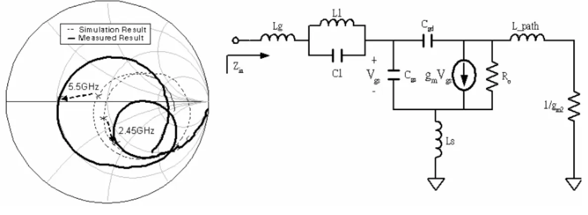
(59) Chapter 4. 43. Chapter 4 Dual-Band Front-End Circuit This chapter presents a fully on-chip dual-band front-end circuit which is fabricated by TSMC 0.18 m RF CMOS technology.. 4.1 Introduction Multi-standard or multi-band radio frequency transceivers are predicted to play a critical role in wireless communications. It is desirable to combine two or more bands and standards in one transceiver [6]. The principal challenge in this task arises from the stringent cost and form-factor requirements. Thus, both the architecture design and the frequency planning of the multi-standard or multi-band transceiver demand careful study and numerous iterations. The direct conversion receiver (DCR) has gained considerable attention recently because it reduce the need for crystal of ceramic filters and other external components, which enables a higher level of integration than traditional heterodyne architecture. However, the well known problems of local oscillator (LO) self-mixing, second-order inter-modulation (IM2), and flicker noise remain as serious obstacles to be overcome when adopting the DCR architecture. In this work, a new DCR dual-band front-end is designed and introduced. The front-end can receive signals from two bands and down convert to base band directly. The front-end circuit includes a concurrent dual-band LNA, gain control stage, high linearity mixer and the high-pass load to develop DC offset problems..
(60) Chapter 4. 44. 4.2 Principle of the Circuit Design In this section, the design principle of the DCR dual-band front-end circuit with variable gain is introduced. Fig.4.1 is the schematic of the circuit of the front-end circuit. The principle emphasizes on the features of each block, which include concurrent dual-band LNA, gain control stage, CMOS pair mixer and the high-pass load.. Fig.4.1. Schematic of the DCR Dual-Band Front-End Circuit with Variable Gain. 4.2.1 Concurrent Dual-Band LNA From previous concurrent dual-band LNA design, measured data show some deviation from simulation result. It can be observed from the S11 Smith chart that unexpected parasitic of the path between the first stage and the cascoded one occurs such that the S11 response is far from 50-Ω at 5-GHz band. The degradation of the noise figure may be due to bad input impedance matching of input stage at 5-GHz band. To solve these problems, a modified concurrent dual-band LNA circuit as shown in.
(61) Chapter 4. 45. Fig.4.2 is designed. The matching network is modified to achieve on-board measurement. The path between the first stage and the cascoded one is considered and shorten.. Modified Concurrent Dual-Band LNA. The method of input matching is similar to that of the method introduced in Chap 3.2. If the capacitance C gd is neglected the input impedance can be expressed as in the following. Z in = sLbond +. g L1 1 1 − 2 ) // m Ls + s ( Ls + 2 sC pad C gs 1 − ω L1C1 ω C gs. (4-1).
(62) Chapter 4. 46. where if Cpad is small enough to be neglected, the input impedance can be re-expressed as. Z in ≈ ω t Ls + j (ωLbond + ωLs +. ωL1 1 − 2 ) = R S = 50Ω 2 1 − ω L1C1 ω C gs. where the R S is the source impedance, typically 50. (4-2). in the RF design, and the. image part of the input impedance will be zero at the two desired resonance frequencies.. 4.2.2 Variable Gain Stage. Fig.4.2. Variable Gain Stage. Fig.4.3 is the architecture of the variable gain stage. The variable gain function is implemented by a current-stealing transistor M3. Controlled by the voltage V_Gain, the transistor affects the signal current level from RF_in to RF_out such that the overall system gain varies. As the voltage of control node V_Gain is set from low to high, the transistor M3 turns on and the impedance Z0 turns from high to low, then the signal current changes.
(63) Chapter 4. 47. to flow into the transistor M3. This method of gain control determines the same noise figure in each gain conditions and consumes no power. The capacitors C4 and C5 are used for DC block.. 4.2.3 CMOS Pair Mixer. Fig.4.3. CMOS Pair Mixer. It is critical to design a mixer of high linearity. A composite CMOS pair is implemented for this purpose, as shown in Fig.4.4 [8]. The RF signal is coupled to the source port of the switching transistors, M6 and M7, by a PMOS source follower configuration with a large aspect ratio. Driven by a differential LO signal, the mixer.
(64) Chapter 4. 48. generates different IF signal. The CMOS pair shown in Fig. 4.5 behaves like a single transistor under the condition of VG − V S > V req as following. Id =. k eq 2. (VG − VS − Vteq ) 2. (4-3). where. 1 1 1 = + k eq kn kp. (4-4). Vteq = Vtn + Vtp. (4-5). Fig.4.4. Single Transistor and the CMOS pair. The architecture of CMOS pair mixer provides higher linearity than traditional Gilbert mixer by removing the stage of trans-conductance. Also, such a CMOS pair mixer is applicable to broadband operation.. 4.2.4 High-Pass Load DC-offset is a severe issue in the DCR architecture. The sources of DC-offset.
(65) Chapter 4. 49. can be mainly categorized into three parts: (1) self-mixing due to LO leakage, (2) self-mixing due to large interferer in RF port, and (3) component mismatch. The third part can be solved by digital parts, but the first and second parts are not easily solved. Therefore, in this circuit a high-pass load as shown in Fig. 4.6 is applied to decrease the signal level near DC to reduce the DC-offset level.. Fig.4.5. High-Pass Load. The circuit shown in Fig. 4.7 (a) is the basic architecture of high-pass load and Fig. 4.7 (b) is its equivalent model. The impedance of load can be derived from Fig.4.7 (b) as in the following. ZL = (. 1 + sR f CT Ro R (1 + sC d Ro ) 1 + R1 ) //( ) )(1 + 1 ) //( R f + gm Ro 1 + sCT 1 + sC d Ro. The frequency response is analyzed in this manner. As. (4-6). is lower than 1/RfCT, the. impedance ZL can be simplified as following. ZL ≈ (. R 1 )(1 + 1 ) gm Ro. if Rf and (Ro+R1) are extremely large. As. (4-7) is higher than 1/RfCT but lower than. 1/RoCd, the impedance ZL can be approximated as Z L ≈ Ro + R1. (4-8).
(66) Chapter 4. If. 50. is higher than 1/RoCd, the impedance ZL can be further approximated as. Z L ≈ R1. (4-9). Therefore, the circuit is a high-pass load for frequency higher then 1/2 RfCT.. (a). (b). Fig.4.6. (a) Basic High-Pass Load (b) Equivalent Model. For wireless LAN applications the IF bands are available for the frequency higher than about 100 kHz. So there is an extremely large capacitor needed. The technique of Miller capacitor amplifier shown in Fig. 4.8 is applied to amplify the capacitor CM1. The capacitance looking from node X will be (1+Av) times larger than the capacitance of CM1. Fig.4.7. Miller Capacitor Amplifier.
(67) Chapter 4. 51. 4.3 Chip Implementation and Measured Result 4.3.1 Microphotograph of Chip. Fig.4.8. Microphotograph of Dual-Band Front-End. The microphotograph of the entire front-end circuit is shown in Fig.4.9. The circuit is fabricated in the TSMC 0.18um CMOS technology. The die area including bonding pads is 1.5 mm by 0.9 mm. The total die area is 1.35 mm2. The RF input is placed on the left side, the LO input is placed on the down side and the IF output is placed on the up side of the chip. The placement of pads is considered for the on-board measurement. In order to minimize the effect of substrate noise on the system, a solid ground plane, constructed using a low resistive metal-1 material, is placed between the signal pads (metal-5 and metal-6) and the substrate. On the other hand, there are many ground pads to minimize the effect of bond-wire.. 4.3.2 Measurement and Simulation Result Measurement is conducted by on-board. A unit gain output buffer is applied for the.
(68) Chapter 4. 52. measurement. Fig.4.10 (a) is the PCB layout of front-end circuit and Fig.4.10 (b) is the PCB layout of unit gain buffer. There is a resistor of 50. for matching between the. output of unit gain buffer and the spectrum analyzer. Therefore, the measured conversion gain is 6dB lower than actual one. The measured input return loss is plotted in Fig.4.11 together with the simulation result for comparison. The measured data of lower band drifts to 2.6-GHz may be due to the effects of bond-wire. As shown in Fig.4.12 (a) and (b), the simulated conversion gains achieve 25.6 dB at 2.45-GHz and 25 dB at 5.5-GHz. And the signal levels near DC degrade 19 and 15 dB at 2.45 and 5.5-GHz bands, respectively. The maximum gain variations achieve 20 and 17 dB, respectively. Fig. 4.14 shows the noise figure versus IF frequency of average 8 and 7dB, which LO operate at 2.45 and 5.5-GHz, respectively. The measured conversion gain at 2.6-GHz is shown in Fig.4.13. The conversion gain achieves 25dB at 1-MHz IF band. Because the operating DC voltage of LO port is changed from 1.2V to 0.9V to enhance the characteristic of switch, the bandwidth of conversion gain degrades. The gain of Miller capacitor amplifier degrades and the lower corner frequency drifts from 60-kHz to 250-kHz. Linearity analysis is conducted by the two-tone test. The two-tone test simulation result of the third-order inter-modulation distortion and the 1-dB gain compression at 2.45 and 5.5-GHz are plotted in Fig. 4.15 (a) and (b). The IIP3 of entire front-end circuit is -16 dBm at 2.45-GHz and -13 dBm at 5.5-GHz. The 1-dB gain compression point is -35 dBm and -33 dBm at 2.45 and 5.5-GHz. The measured results of linearity at 2.6-GHz is shown in Fig. 4.16. The signals of two tone test are at 2.6015-GHz and 2.6025-GHz. The measured 1-dB gain compression point is -29dBm and the measured IIP3 is -10dBm. Fig. 4.17 shows the measured IIP2 of front-end circuit is -11dBm. The total power of the LNA circuit dissipates 21 mW with a power supply 1.8V..
(69) Chapter 4. 53. The comparison of dual-band front-end circuit and previously publish work is summarized in TABLE. TABLE.II.. .. Comparison of dual-band front-end circuit and previously publish work. Freq [GHz] Gain [dB] Max. Gain Variation [dB] S11 [dB] NF [dB] P-1dB [dBm] IIP3 [dBm] Area [mm2] Pw [mW]. This work. 2.6 5.5 25 25 17 17 -16 -16 8 7 -29 -33 -10 -13 1.35 21. [9] 1.57 2.1 27.5 34 N/A -13 -15 4.7 4.4 N/A -28 -23 4.6 N/A. [10] 0.9 39.5 27.5 -12 2.3 -29 -19. 2.1 33 27.5 -18 4.3 -25 -14.5 3.5 22.5. [11] [12] 2.4 20.3 6 -19 7.2 N/A -9.5 20 116. ps. The red data is the simulation results and the black one is the measured data. 5.2 16.5 N/A <-10 8.5 -24 -13 3 22.4.
(70) Chapter 4. 54. Fig.4.9. PCB layout of (a) Front-End Circuit (b) Unit Gain Output Buffer.
(71) Chapter 4. Fig.4.10. Input Return Loss of Dual-Band Front-End Circuit. 55.
(72) Chapter 4. 56. Fig.4.11. Simulation Results of Conversion Gain (a) 2.45GHz (b) 5.5GHz.
(73) Chapter 4. Fig.4.12. Measured Results of Conversion Gain at 2.6GHz. 57.
(74) Chapter 4. 58. Fig.4.13. Simulation Results of Noise Figure (a) 2.45GHz (b) 5.5GHz.
(75) Chapter 4. Fig.4.14. Simulation Results of Linearity (a) 2.45GHz (b) 5.5GHz. 59.
(76) Chapter 4. 60. Fig.4.15. Measured Results of IIP3 at 2.6GHz. Fig.4.16. Measured Results of IIP2 at 2.6GHz.
(77) Chapter 5. 61. Chapter 5 SUMMARY AND FUTURE WORK 5.1 Summary In Chapter 2, the architecture of receiver and RF protocols of wireless LAN are introduced. Some theoretical MOSFET noise model and noise theory are presented. Besides the problem of noise, linearity is another critical issue to design a superior front-end circuit. Also, the blocks in the front-end such as LNA and mixer are discussed. In Chapter 3, a concurrent dual-band step-gain LNA is analyzed and implemented in a standard 0.18µm CMOS process. Although, measured result shows some discrepancies of the performance. Measured data shows that the concurrent dual-band LNA achieves maximum power gain (S21) of 11 and 8.5 dB at 2.45 and 5.5-GHz bands, respectively. Input return loss (S11) and output return loss (S22) are worse than -10dB. The LNA achieves maximum gain variation of 13 and 15 dB, and noise figure of 4 and 5.4 dB at 2.45 and 5.5-GHz, respectively. The total power dissipation is 14.6mW with a power supply 1.5V. In Chapter 4, a dual-band front-end circuit, intended for use in the receiver path of the wireless LAN systems is then designed in a standard 0.18µm CMOS process. The modified LNA achieves better input impedance matching and revises the step gain function by a current-stealing transistor. A direct conversion CMOS pair mixer with high-pass load is added to complete the front-end. The CMOS pair mixer provides higher linearity than traditional Gilbert mixer and the high-pass load minimizes the problem of DC-offset. The measured data shows the operating.
(78) Chapter 5. 62. frequency of lower band deviates from 2.45-GHz to 2.6GHz. The simulated conversion gains achieve higher than 25dB at both frequency bands and degrade more than 15dB near DC. The maximum gain variations achieve 20 and 17dB at 2.45 and 5.5GHz. The input return losses are better than 10 dB, and average noise figures are 8 and 7dB in the 2.4 and 5GHz band, respectively, while the entire circuit consumes only 21 mW with a power supply of 1.8V.. 5.2 Future Work The noise figure of the concurrent dual-band LNA is poor and far from simulation result at high frequency. The discrepancy may be due to the inaccuracy of the noise model and low trans-conductance of the input stage. Also, the measured power gain is poor than simulation result. Although dual-band front-end circuit can achieve adequate conversion gain and the function of down conversion while consuming low power and small chip area. The measured data shows the performance is a little far from the simulation result at high frequency. The discrepancy may be due to the inaccuracy of the MOSFET model and some bond-wire effects. Therefore, how to further decrease the difference between simulation and measured data become a challenge. Also, to complete the overall receiver by adding dual-band VCO is another challenge in the future..
(79) References. 63. REFERENCES [1]. Thomas H. Lee, The Design of CMOS Radio-Frequency Integrated Circuits, Cambridge, U.K.: Cambridge Univ. Press, 1998.. [2]. A. van der Ziel, Noise in Solid State Device and Circuits, New York:Wiley, 1986. [3]. Behzad Razavi, RF Microeletronics, Prentice Hall PTR, 1998. [4]. D.K. Shaeffer and T.H.Lee, ”A 1.5V, 1.5GHz CMOS Low Noise Amplifier,” IEEE Journal of Solid-State Circuit, vol. 32, no.5, pp.745-759, May.1997.. [5]. H. Hashemi and A. Hajimiri, “Concurrent Dual-Band CMOS Low Noise Amplifiers and Receiver Architectures,” VLSI Circuits Symp. Dig., pp.247-250, June. 2001.. [6]. S. Wu and B. Razavi, “A 900-MHz/1.8-GHz CMOS Receiver for Dual-Band Applications,” IEEE J. Solid-State Circuits, Dec. 1998, vol. 33, no. 12, pp. 2178-2185.. [7]. Keng Leong Fong, “Dual-Band High-Linearity Variable-Gain Low Noise Amplifiers for Wireless Applications,” IEEE International Solid-State Circuit Dig., pp.224-225, Feb. 1999. [8]. R. F. Salem, S. H. Galal, M. S. Tawfik and H. F. Ragaie, “A New Highly Linear CMOS Mixer Suitable for Deep Submicron Technologies,” Electronics, Circuits and Systems 9th International Conference, vol. 1, pp. 81-84, Sept. 2002.. [9]. M. Y. Wang, R. B. Sheen and T. C. Chen, “A Dual-Band RF Front-End for WCDMA and GPS Applications,” ISCAS Symp., vol. 4, pp. 113-116, May 2002.. [10]. J. Ryynanen, K. Kivekas, J. Jussila, A. Parssinen and Kari A.I. Halonen, “A Dual-Band RF Front-End for WCDMA and GSM Applications,” IEEE J. Solid-State Circuits, vol. 36, no. 8, pp. 1198-1204, Aug. 2001.. [11]. F. Behbahani, J. C. Leete, Y. Kishigami, A. Roithmeier, K. Hoshino and A. A. Abidi, “A 2.4-GHz Low-IF Receiver for Wideband WLAN in 0.6-µm CMOS-Architecture and Front-End,” IEEE J. Solid-State Circuits, vol. 35, no. 12, pp 1908-1916, Dec. 2000..
(80) Reference. [12]. 64. C. Y. Wu and C. Y. Chou, “A 5-GHz CMOS Double-Quadrature Receiver Front-End With Single-Stage Quadrature Generator,” IEEE J. Solid-State Circuits, vol. 39, no. 3, pp 519-521, March, 2004..
(81) VITA. 65. : : ( 84. 9. ~ 87. 6. ). ( 87. 9. ~ 91. 6. ). ( 91. 9. ~ 93. 6. ).
(82)
數據
相關文件
Move fast and try not to make the elastic band fall on the ground?. Now move with
接收器: 目前敲擊回音法所採用的接收 器為一種寬頻的位移接收器 其與物體表
Wang, Solving pseudomonotone variational inequalities and pseudocon- vex optimization problems using the projection neural network, IEEE Transactions on Neural Networks 17
Define instead the imaginary.. potential, magnetic field, lattice…) Dirac-BdG Hamiltonian:. with small, and matrix
Monopolies in synchronous distributed systems (Peleg 1998; Peleg
The economy of Macao expanded by 21.1% in real terms in the third quarter of 2011, attributable to the increase in exports of services, private consumption expenditure and
Due to a definition of noise factor (in this case) as the ratio of noise powers on the output versus on the input, when a resistor in room temperature ( T 0 =290 K) generates the
• The band-pass filter at the frontend filters out out-of-band signals and
