1
行政院國家科學委員會研究計畫成果報告
計畫題目: 深次微米射頻元件
計畫編號: NSC 90-2215-E-009-052
執行期限:90年8月1日至 91年7月31日
主持人:荊鳳德 教授 執行單位:交通大學電子工程系 學生:詹歸娣
中文摘要
為了達到高效能及極佳的高頻特性,在製作 0.5 、 0.25 以 及 0.18 微 米 之 高 頻 電 晶 體 中 , 利 用 raised source/drain的方法來實現,並且,於接點處 成長低阻值的矽化鈷,不僅減小閘極阻抗和產生 最大功率增益,進而,避免其在最高工作頻率之 不良影響,另則,使用多指的閘極結構來增大其 電流值並可有降低閘極阻抗之功用,在完成對射 頻元件之設計及製程後,即對三種不同尺寸的電 晶體分別做了直流與高頻的電性量測,並針對所 得的量測數據使用模擬工具進行分析與比較。 而數值分析之結果顯示,其高頻效能改善的 幅度也漸趨和緩而達到飽和,是隨著電晶尺寸的 微縮化。再進一步,利用簡單但有效的高頻電晶 體 等 效 電 路 模 型 加 以 分 析 , 發 現 造 成 這 趨 勢 特 性,主要之因素為其電晶體閘極與汲極間的寄生 電容Cgd 之影響以及高頻的非穩態效應(non-quasi static effect)所造成,因為這些效應並未隨著閘極 長度的微縮化而減小,而影響了深次微米射頻元 件之高頻特性。 關鍵詞: 高頻電晶體,電晶體微縮化,非穩態效應 AbstractFor achieving the optimum characteristics of RF performance, taking the methods of raised source/drain to fabricate at the Deep sub-µm RF Devices of 0.5µm 0.25µm 0.18µm Furthermore, the growth of CoSi2 can help producing the higher power
gain by lower resistance and using the technique of the multiple gate fingers due to enhance the current . After the device process, the measured numeric of DC and RF is to be compared and analyzed with simulation.
Obviously, it is found the measured RF performance of 0.5, 0.25, and 0.18 µm MOSFETs gradually saturates as scaling down, which can be explained by the derived analytical equation and simulation. It is reasonable that the overlap Cgd and
non-quasi-static effect are the main factors but scales much slower than Lg.
This paper has been submitted to IEEE MTT-S 2000.
Keywords: RF MOSFET, scaling down, RF performance
一、簡介
Although Si RF MOSFETs has the advantages of rapid technology evolution and low production cost, it is still not clear where is the limitation of MOSFETs [1], and whether Si BJT [2] or even III-V technology should be used at higher frequencies. In this paper, we have analyzed the fabricated 0.5, 0.25, and 0.18 µm MOSFETs, and discuss performance limiting factors as scaling down using our derived analytical equation and numerical device simulation. We have found that the RF performance improvement gradually saturates as scaling down, which is observed by both experimental data and our analysis. The gate-drain overlap capacitance (Cgdo) is the key factor for Gmax
and fmax; unfortunately, it is difficult to proportionally
scale down as Lg due to lateral diffusion of
source-drain implants. The non-quasi-static (NQS) effect will also reduce the H21, ft, and maximum available gain
(MAG). Our work can help to understand the performance limitation of MOSFET scaling and further choose of device operated at high frequencies.
二、實驗方法
Multiple fingered 0.5, 0.25, and 0.18 µm MOSFETs are fabricated on standard ~10 Ω-cm Si substrate with gate width of 200-250 µm and on-wafer probe layout. The multiple gate fingers with low resistivity CoSi2 [3] can achieve a reasonable power
level and reduce the extrinsic gate resistance that is important for Gmax and fmax. Then, S-parameters were
measured up to 18 GHz using a CASCADE on-wafer probe, a network analyzer, and de-embedded from dummy devices. A matrix of different size of transistors and capacitors is used to extract device
2 parameters for further analysis using modified BSIM3v3 MOSFETs model in SPICE..
三、結論與討論
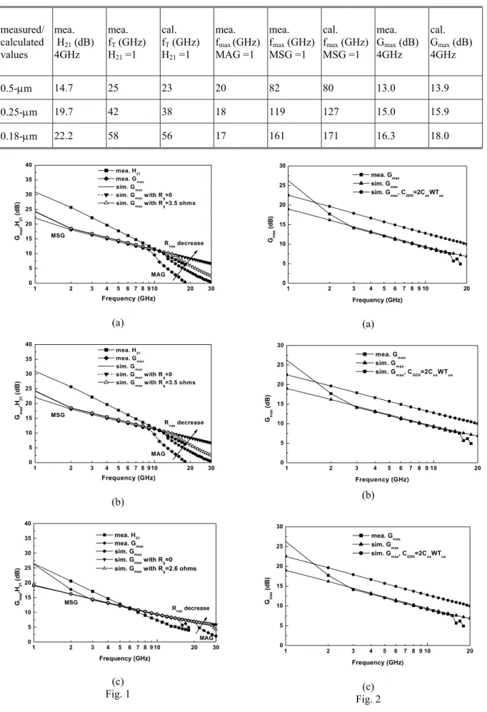
The measured frequency response of H21 and Gmax
according to the equations (1) to (4) is plottedin Fig. 1 and summarized in Table 1.
2 2 1 1 ) ( 2 1 1 ) ( 2 + − − + = + − − + = ov s ov nqs m ov g sat gd gs gd nqs m gd gs m t L L L R g L L v C C C R g C C g f π π (1) ) 1 ( )] ( 1 [ ) 1 ( 2 2 12 21 max − − + + − = − − = K K jwC C C jwR g jwC K K S S G gd gs gd nqs m gd (2) 2 1 max,
)
(
2
1
2
1
C
R
g
C
R
g
C
g
f
g m g m gd m MSG−
=
=π
(3) gd gs C C C= 1+ (4)It is important to notice that the measured H21, ft,
Gmax, and fmax gradually saturate as device scaling
down. The saturation rate is faster for Gmax and a
reducing fmax is even observed.
Furthermore, the measured H21 and ft are about
50% lower than the calculated value from conventional equation of gm/2πCgs or vsat/2π(Lg-2Lov),
where Lov is
the gate-drain overlap length. We have therefore derived a more accurate H21 and ft (at H21=1)
equations using modified BSIM3v3 equivalent circuit model and including the NQS effect.
Although the Rnqs related term in H21 is negligible at
low frequency, it becomes more important as increasing frequency near ft. Good matching between
measured and simulated ft in Table 1 can only be
obtained by considering the NQS effect. Because of the additional term, ft increases slower than 1/ Lg
scaling down.
Similar large difference of 300%-350% exists in the measured and calculated fmax using the well-known
equation of (ft/8πRgCgd)1/2. This difference is because
the above equation is derived from the unilateral gain with a constant gain roll-off while Gmax changes to
30-40dB/decade decrease in MAG
To further analyze the frequency response, we have also derived Gmax and fmax by using the equivalent
circuit modeling and including the NQS effect. From derived Gmax, Cgd related pole gives the 10dB/decade
Gmax roll-off in MSG, while the large slope of
~30-40dB/decade in MAG is due to additional poles in K or the NQS effect on gm.
Although similar method can be used to calculate fmax at Gmax=1, unfortunately, no analytical solution
can be derived for fmax. In contrast, analytical fmax at
MSG=1 can be obtained when (K− K2−1) =1,
we have therefore analyzed fmax,MSG=1 to obtain a
better understand of device design parameters on
fmax,MSG=1.
Good agreement between the measured and calculated fmax,MSG=1 is achieved and shown in Table 1.
The primirary parameter for fmax,MSG=1 increase is due
to the gm increase and Cgd decrease. In fact, Cgd is
dominated by the Cgdo that is difficult to
proportionally scale down with Lg.
W e h a v e a l s o u s e d numerical device simulation for further analysis. We have studied the NQS effect on Gmax and fmax. As shown in Fig. 1, the
MAG increases with decreasing Rnqs and eventually
gives Gmax the same 10dB/decade roll-off as MSG
when Rnqs equals 0. Therefore, the NQS effect is
responsible for the transition from MSG to MAG. Because Rnqs is inversely related to Cgs, a higher
dielectric or thinner gate thickness is required to improve the high frequency gain.
On the other hand, Gmax has a simple analytical
solution in the most useful MSG region for amplifier design. Because the Rnqs(Cgs+Cgd) related zeros are
effective only at high frequencies, Gmax in MSG can
be further simplified and expressed by gm/ωCgd or
vsat/ωLov. The numerical simulation result is shown in
Fig. 2. It is clear that the reduction of Cgdo leads to a
higher Gmax and fmax. However, the difference between
the ideal 2CoxWtox and the measured data is larger as
scaling down.
Here, a minimum Cgdo of CoxWLov (Lov=2tox) [4] is
required in order to develop a reproducible and manufacturable process, where Cox and tox are the gate
capacitance and oxide thickness, respectively. Although down scaling gives a smaller Lg and a
higher Cox, limited Gmax improvement in MSG is due
to the slower scalable Lov. The reason for Lov failing to
follow tox scaling down in deep sub-µm devices is due
to the lateral diffusion from source and drain impurities. High temperature annealing after source and drain implantation is necessary to reduce the junction leakage but largely increases the lateral diffusion. The formation of silicide junction also requires high temperature RTA. Because of the combined small Gmax and K factor improvement,
limited fmax improvement as device scaling down can
be expected.
The smaller increase of measured Gmax than
calculated value in Table 1 as down scaling may be due to the parasitic effect neglected in our device model.
四、參考文獻
[1] M. C. Ho, F. Brauchler, and J. Y. Yang, “Scalable RF Si MOSFET distributed lumped element model based on BSIM3v3,” Electronics Lett., vol. 33, no. 23, pp. 1992-1993, 1997.
[2] S. Niel, O. Rozeau, L. Ailloud, C. Hernandez, P. Llinares, M. Guillermet, J. Kirtsch , A. Monroy, J. de Pontcharra, G. Auvert, B. Blanchard, M.
3 Mouis, G. Vincent, and A. Chantre, “A 54 GHz fmax implanted base 0.35µm single-polysilicon
bipolar technology,” in IEDM Tech. Dig., 1997, pp. 807-810.
[3] Y. H. Wu, W. J. Chen, S. L. Chang, A. Chin, S. Gwo, and C. Tsai, “Improved electrical characteristics of CoSi2 using HF-vapor
pretreatment,” IEEE Electron Device Lett., vol. 20, no. 5, 200, 1999.
[4] T. Y. Chan, A. T. Wu, P. K. Ko, and C. Hu, “Effects of the gate-to-drain/source overlap on MOSFET characteristics,” IEEE Electron Device Lett., vol. 8, pp. 326-328, 1987.
[5] A. Chin, K. Lee, B. C. Lin, and S. Horng, "Picosecond photoresponse of carriers in Si ion-implanted Si," Appl. Phys. Lett. 69, 653 (1996). [6] A. Chin, W. J. Chen, F. Ganikhanov, G.-R. Lin,
J.-M. Shieh, C.-L. Pan, and K. C. Hsieh, "Microstructure and sub-ps photoresponse in GaAs grown by molecular beam epitaxy at very low temperatures," Appl. Phys. Lett. 69, 397 (1996).
[7] H. H. Wang, J. F. Whitaker, A. Chin, J. Mazurowski, and J. M. Ballingall, "Subpicosecond carrier response of unannealed low-temperature grown GaAs vs temperature," J. Electron Materials 22, 1461 (1993).
[8] A. Chin, K. Lee, W. J. Chen, Y. S. Zhang, S. Horng, and J. H. Kao, “Picosecond
photoresponse of carriers on Si,” 38th Electronic
Materials Conference (EMC) Santa Barbara, CA, June 1996.
Figure Captions:
Table I Measured and calculated RF data.
Fig.1 Gain-frequency response for measured and simulated (a) 0.18, (b) 0.25, and (c) 0.5µm MOSFETs.
Fig.2 The effect of reducing Cgdo on gain-frequency
response for (a) 0.18, (b) 0.25, and (c) 0.5 µm MOSFETs.
4
Table I. Measured and calculated RF data.
1 2 3 4 5 6 7 8 910 20 30 0 5 10 15 20 25 30 35 40 Rnqs decrease MSG MAG mea. H21 mea. Gmax sim. Gmax
sim. Gmax with Rg=0 sim. Gmax with Rg=3.5 ohms
Gma x ,H21 (dB ) Frequency (GHz) (a) 1 2 3 4 5 6 7 8 910 20 30 0 5 10 15 20 25 30 35 40 Rnqs decrease MSG MAG mea. H21 mea. Gmax sim. Gmax
sim. Gmax with Rg=0
sim. Gmax with Rg=3.5 ohms
Gma x ,H21 (dB ) Frequency (GHz) (b) 1 2 3 4 5 6 7 8 9 10 20 30 0 5 10 15 20 25 30 35 40 MAG MSG Rnqs decrease mea. H21 mea. Gmax sim. Gmax
sim. Gmax with Rg=0 sim. Gmax with Rg=2.6 ohms
Gma x ,H21 (d B ) Frequency (GHz) (c) Fig. 1 1 2 3 4 5 6 7 8 9 10 20 0 5 10 15 20 25 30 mea. Gmax sim. Gmax sim. Gmax, CGD0=2CoxWTox Gma x (dB ) Frequency (GHz) (a) 1 2 3 4 5 6 7 8 9 10 20 0 5 10 15 20 25 30 mea. Gmax sim. Gmax sim. Gmax, CGD0=2CoxWTox Gma x (d B ) Frequency (GHz) (b) 1 2 3 4 5 6 7 8 9 10 20 0 5 10 15 20 25 30 mea. Gmax sim. Gmax sim. Gmax, CGD0=2CoxWTox Gma x (dB ) Frequency (GHz) (c) Fig. 2 measured/ calculated values mea. H21 (dB) 4GHz mea. fT (GHz) H21 =1 cal. fT (GHz) H21 =1 mea. fmax (GHz) MAG =1 mea. fmax (GHz) MSG =1 cal. fmax (GHz) MSG =1 mea. Gmax (dB) 4GHz cal. Gmax (dB) 4GHz 0.5-µm 14.7 25 23 20 82 80 13.0 13.9 0.25-µm 19.7 42 38 18 119 127 15.0 15.9 0.18-µm 22.2 58 56 17 161 171 16.3 18.0