國 立 交 通 大 學
顯示科技研究所
碩士論文
液晶顯示器之奈米及尖端型電極增強型
電漿平面光源研究與開發
Development of the Nano-Tip and the Conical Electrode
Enhanced Plasma Flat Lamps for Liquid Crystal Display
研究生:蔡柏全
指導教授:金星吾 教授
液晶顯示器之奈米及尖端型電極增強型
電漿平面光源研究與開發
Development of the Nano-Tip and the Conical Electrode
Enhanced Plasma Flat Lamps for Liquid Crystal Display
研 究 生: 蔡柏全
Student:
Po-Chuan
Tsai
指導教授: 金星吾
Advisor:
Dr.
Sung-O
Kim
國立交通大學
顯示科技研究所
碩士論文
A Thesis
Submitted to Display Institute
College of Electrical Engineering and Computer Science
National Chiao-Tung University
in Partial Fulfillment of the Requirements
for the Degree of Master
in
Display Institute
August 2008
Hsinchu, Taiwan, Republic of China.
中華民國 九十七年 八月
液晶顯示器之奈米及尖端型電極增強型
電漿平面光源研究與開發
研究生:蔡柏全 指導教授:金星吾 博士
國立交通大學顯示科技研究所碩士班
摘要
隨著電腦科技與網路普及所帶來對人類生活品質的衝擊,各樣具有輕薄短 小、低耗功率等顯示器的需求越來越高,近年來更邁入大尺寸家用型電視市場。 近年來,隨著台灣廠商的開發和努力下,液晶電視已經逐漸的取代傳統映像管電 視機,成為家家戶戶必備之影音顯示設備。輕薄且省空間的懸掛式,以及高畫質 電視等特性,液晶電視的與電漿電視等大型尺寸的競爭下,也逐漸引人注目。然 而,由於液晶面板屬於非自發光的顯示器,故背光源的開發便顯得十分關鍵。冷 陰極管光源目前為最主要的背光的光源。由於各國對汞有毒物質的使用限制日趨 嚴格,故在此我們提出了針對無汞環境議題下,提出了新式的無汞平面光源。 此研究的重點在於利用惰性氣體的放電取代汞蒸氣,在細微的放電間隙下和 直流脈衝電壓的驅動下,利用尖端電極所累積電荷所產生的電場增益,提出了 14 吋的奈米尖端形增強型電漿平面光源,並且更延伸開發出進階的 14 吋增強型 尖端電極電漿平面光源。此平面光源再操作在 260 福特的驅動電壓和 50 脫爾的 且達到最大為 7780 坎得拉每平方米的亮度以及 44 流明每瓦的發光效率。此研 究不僅僅改善了驅動電壓和發光效率,也降低的成本和改善了環境保護的議題。Development of the Nano-Tip and the Conical Electrode
Enhanced Plasma Flat Lamps for Liquid Crystal Display
Student: Po-Chuan Tsai Advisor: Dr. Sung-O Kim
Department of Photonics and Display Institute, National Chiao-Tung University
Abstract
As the impacts to the life qualities of people from the high technology, varieties flat panel display which provided thin, light, and low power consumption are getting important, especially in liquid crystal display (LCD). From the mobile phone to monitor even television applications, LCD plays an important role in flat panel display today. LCD panel has successfully replaced the traditional cathode ray tube (CRT) in our daily life. Due to the non-emissive feature of LCD, the development of the backlight module is getting more important. The cold cathode fluorescent lamp (CCFL) is used commonly as the backlight units. However, the use of the mercury according to the environmental protection issue as well as the lifetime in CCFL need to advance more, several kinds of the mercury-free lamp are developed significantly.
The aiming of this study is that we proposed a fabricated 14 inch mercury-free nano-tips enhanced plasma flat lamps (NTL) using the xenon as a discharge gas instead of mercury vapor. With the properties of the needle like electrode of the nano-tip and tiny gap between both ITO electrode and rear electrode, the direct current (DC) pulse bipolar waveform is applied and the electric field is enhanced locally for the low operating voltage and high luminance and luminous efficiency. We also proposed the advanced 14 inch mercury-free conical electrode enhanced plasma flat lamp with conical electrode to replace the nano-tip and it achieved 7649 cd/m2 of luminance and 44 lm/W of luminous efficiency with 50 torr xenon gas filled at 260 V. Not only the environmental issue, driving voltage and luminance, but the cost of the CPL is improved compared the NTL and the other conventional mercury-free flat lamp.
致謝
首先,我要感謝我有這個機會能在交通大學的研究所當中學習,除了專業相 關知識上的長進,更在人生歷練中和如何做人處事往前一大步。我還要感謝金星 吾指導教授在學業、研究以及英文方面的指導,並且讓我在研究生活當中有更深 的國際觀也在團隊當中學習到團隊精神與合作的重要。 除此之外,我要感謝與我一起打拼奮鬥的好伙伴-陳逸棠。當初的兩人小組 實驗室,靠著互相的打氣和研究,讓我深深體會到同伴的重要。謝謝你們在日常 生活中的照顧與包容,更感謝你在實驗上的幫助與鼓勵,兩年的共同生活讓我從 你身上有許多深刻的學習;我還要感謝實驗室助理小姐們的細心幫忙與協助;中 華映管核心技術處的莫啟能處長,謝謝您對於研究上的提攜和研究以外的做人做 事的道理,還有吳上智、江美昭以及李宗陽等工程師等在專業上面的協助。 最後但也是最重要的,我要感謝我親愛的父母以及阿公,謝謝你們愛的包 容、鼓勵與無私心的支持;我更要感謝我的女朋友蔡孟辰,謝謝妳陪我走過這段 時光,感謝妳在低潮時的陪伴與鼓勵,感謝妳百分百的支持與愛,和不厭其煩的 傾聽,讓我能咬緊牙關完成研究所的課程與實驗;我要再一次感謝在這篇論文中 所有曾經幫助過我的人,並且讓這份喜悅與每位關心我的人分享。Table of Contents
Abstract (Chinese) ...iii
Abstract (English) ...iv
Acknowledgements ...v
Table of contents...vi
Figure captions ...viii
List of Tables ...xii
Chapter 1
INTRODUCCTION
1.1. Flat panel display (FTP)... 11.2. LCD backlight module ... 2
1.3. LCD backlight units ... 6
1.3.1 Cold Cathode Fluorescent Lamp (CCFL)………...6
1.3.2 Light emitted diode (LED)……….8
1.3.3 Flat fluorescent lamp (FFL)………10
1.4. Motivation ... 11
1.5. Organization ... 13
Chapter 2
PLASMA THEORY
2.1. Background of the Mercury-free Lamp ... 142.1.1 Planon®……….15
2.1.2 Coplanar type mercury-free lamp………..………..…….16
2.1.3 Dual coplanar type mercury-free lamp………....17
2.2. Gas reactions ... 19
2.2.1 Plasma science………...19
2.2.2 Gas breakdown and reactions………22
2.2.3 VUV generation………...24
2.3.1 Quantum tunnel effect………...26 2.3.2 Fowler-Nordheim equation………..27
Chapter 3
EXPERIMENT
3.1. Introductions ... 30 3.2. Fabrication processes... 33 3.2.1. Substrate preparation………333.2.2. ITO electrode patterning………34
3.2.3. Silver deposition……….37
3.2.4. Dielectric layer deposition………39
3.2.5. Phosphor layer deposition………...41
3.2.6. Panel assembling………42
3.2.7. Sintering process………43
3.3. Experimental setup ... 46
3.3.1. High vacuum system……….46
3.3.2. Driving mechanism………47
3.3.3. BM-7 luminance meter………..48
Chapter 4
RESULTS AND DISCUSSION
4.1. Nano-tips electrode enhanced plasma flat lamp (NTL) ... 504.1.1. Optical properties………..50
4.1.2. I-V characteristics………..52
4.1.3. Luminance and luminous efficiency……….53
4.2. Conical electrode enhanced plasma flat lamp (CPL) ... 57
4.2.1. Structure of the CPL………..57
4.2.2. Optical properties……….…..60
4.2.3. I-V characteristics………..61
4.2.4. Luminance and luminous efficiency……….62
4.3. Backlights comparison ... 63
Chapter 5
CONCLUSIONS
Conclusions...65Figure Captions
Chapter 1: INTRODUCTION
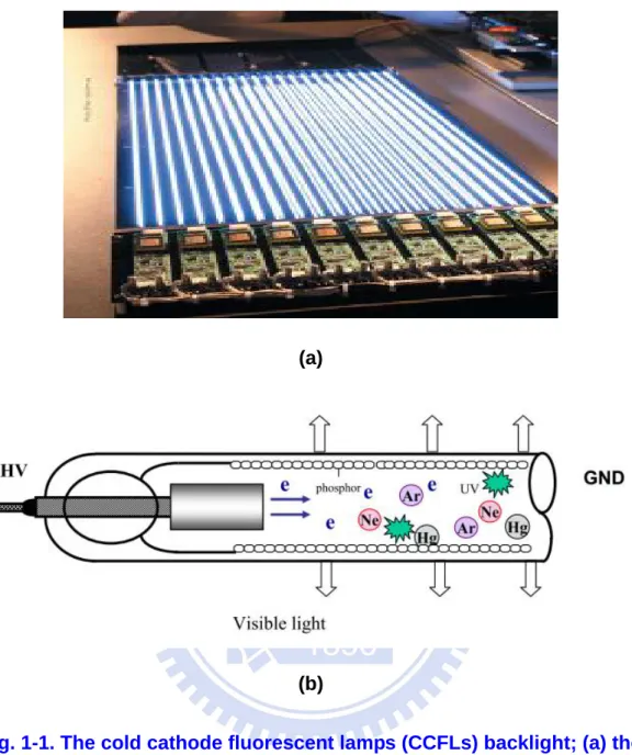
Fig. 1-1. The cold cathode fluorescent lamps (CCFLs) backlight; (a) the photograph of CCFL backlight source ; (b) the cross-sectional
schematic diagram of CCFL………..8 Fig. 1-2. The light emitted diode (LED) backlight; (a) the photograph of the
LED; (b) the cross-sectional schematic diagram of the LED…..……10 Fig. 1-3. The cross-sectional schematic diagram of the mercury-free flat
fluorescent lamp (FFL)……….11
Chapter 2: PLASMA THEORY
Fig. 2-1. (a) The photograph of Planon® mercury-free flat lamp; (b) the
specifications of the Planon® mercury-free flat lamp………..16 Fig. 2-2. (a) The cross-sectional schematic diagram of the coplanar type
mercury-free lamp; (b) the luminance and efficacy of the coplanar type mercury-free lamp as a function of the applied voltage………..17 Fig. 2-3. The cross-sectional schematic diagram of the dual coplanar
mercury-free flat lamp………..18 Fig. 2-4. Luminance and efficiency of the dual coplanar mercury-free flat lamp
as a function of the applied voltage by a 20-kHz, peak voltage 2.8 kV of AC pulse driving………..………..19 Fig. 2-5. Four kinds of matter states in the universe………...………20 Fig. 2-6. The variety applications of the plasma science……….…...………...21
Fig. 2-7. The current-voltage (I-V) characteristics of glow discharge…...……22
Fig. 2-8. (a) The diagram of energy level transition of the xenon gas discharge reactions; (b) the VUV wavelength intensity of the xenon gas
discharge…….………...25 Fig. 2-9. The diagram of energy level and energy density on the surface e of
metal in vacuum while applied field F>0 and F=0..……….27
Chapter 3: EXPERIMENT
Fig. 3-1. The cross-sectional schematic diagram of the nano-tips electrode enhanced plasma flat lamp (NTL)………...………...30 Fig. 3-2. The flowchart of fabricated NTL ..………...33 Fig. 3-3. The glass substrate cleaning before all the processes …………..…34 Fig. 3-4. The flowchart of ITO electrodes patterned on the front panel of the
NTL………..36 Fig. 3-5. The exposure instrument of the ITO electrode patterned ………...36 Fig. 3-6. The photograph of the screen thick printing machine of the silver
electrode deposition………...………...38 Fig. 3-7. Three main parameters: squeegee angle, pressure and speed, of the
screen printing method………..…………...39 Fig. 3-8. The photograph of the screen thick printing machine of the dielectric
layer deposition……….40 Fig. 3-9. The photograph of the phosphor deposition; (a) the photograph of
phosphor paste with magnet agitator; (b) the photograph of nozzle of the spraying instrument………42
Fig. 3-10. The photograph of the sealing glass………..43 Fig. 3-11. The photograph of the panels assembling; (a) the nozzle
to inject with the frit paste; (b) the panel assembled with the clips..……….43 Fig. 3-12. The schematic diagram of the hard-bake furnace (above)
and temperature profile of the hard-bake furnace………45 Fig. 3-13. The photograph of the temperature profile of the
furnace………45 Fig. 3-14. The high vacuum and gas filled system……….47 Fig. 3-15. (a) The photograph of the DC pulse bipolar waveform
generator; (b) the diagram of waveform of the DC pulse bipolar of the supply………..48 Fig. 3-16. The photograph of the BM-7 luminance meter………….49
Chapter 4: RESULTS AND DISCUSSION
Fig. 4-1. The optical appearance of NTL filled with 50 torr, pure xenon gas, under the frequency 50 kHz, current 0.26 A and voltage 260 V……52 Fig. 4-2. The I-V characteristic of NTL of the 50 torr pressure and pure xenon under the 50 kHz frequency of the DC pulse bipolar waveform……53 Fig. 4-3. The Luminance and luminous efficiency on NTL, filled with 50 torr
pure xenon as a function of the applied voltage………..56 Fig. 4-4. The cross-sectional schematic diagram of conical electrode
enhanced plasma flat lamp……….58 Fig. 4-5. The top-viewed schematic diagram of conical electrode enhanced
Fig. 4-6. The optical appearance of the CPL filled with 50 torr, pure xenon gas, under the frequency 50 kHz, current 0.13 A and voltage 260 V……60 Fig. 4-7. The current vs. voltage (I-V) characteristics of the CPL………..……61 Fig. 4-8. The luminance and luminous efficiency of the CPL, filled with 50 torr pure xenon as a function of the applied voltage………..63
List of Tables
Chapter 3: EXPERIMENT
Table 3-1. The specification of fabricated NTL………45 Table 3-2. The condition of driving mechanism………...61
Chapter 4: RESULTS AND DISCUSSION
Table 4-1. The electric results of the NTL……….67 Table 4-2. The specifications of the advanced conical electrode enhanced plasma lamp (CPL)………...72 Table 4-3. The comparisons of fabrication between NTL and CPL………..73 Table 4-4. The electric results of the CPL………...…….75 Table 4-5. The LCD backlight units comparison………..………...77
Chapter 1
INTRODUCTIONS
1.1. Plat panel display (FPD)
With the progress of display technologies from the traditional Cathode Ray Tube (CRT) display, it has successfully promoted to variety of the fantastic display panels with the excellent performance. The performances such as the lifetime, luminance, contrast ratio, view angle, power consumption and cost are still the key factors in display. The CRT display, which was provided the best performances and realized with the most mature manufactured processes, had occupied the most of the market share in the past two decades. Despite these advantages coming from the CRT display, it still had the weak points liked heavy, space-occupied and radiate pollution. To solve these problems, there are several researches which work for the thin, light and small flat panel display is getting more and more important virtually. The followings are provided several conventional flat panel displays nowadays:
1) Liquid crystal display (LCD) 2) Plasma display panel (PDP)
3) Field emission display (FED) 4) Vacuum fluorescent display (VFD) 5) Organic light emitted diodes (OLED)
Despite of the facts that there are so many kinds of the amazing flat panel display, liquid crystal display (LCD), which is progressing away, has to be used commonly used from the personal hand-carried digital devices such as mobile phones, personal digital assist (PDA), digital camera to the larger scale like monitors, personal desktop and laptop computers and, then, the latest tendency is focused on the larger scale TV applications in the world right now. Compared with the CRT display panel, LCD has provided the thin, light, space-saving, low power consumption, radiate pollution-free, long lifetime and semi-conductivity compatibility. The thin film transistors liquid crystal display (TFT-LCD), the most popular technology in LCD, is composed of the backlight modulation, TFT array, color filter array, liquid crystal layers and driving integrated circuits.
one of the components of the LCD. So far, LCD backlight module, which occupied thirty five percents, has been the top two important components in the LCD manufacture. Due to the non self-emissive characteristics the LCD was, the backlight module must attach behind and illuminate the high luminance and uniform distribution as a light source to show the normal images by controlling the liquid crystal rotation. As a result, it affects obviously the high performances including the power consumptions as well as high luminance. LCD panel have been potentially applied to the all kinds of the electronic products, therefore, it is concerned significantly about the consumptions of backlight module and relative components in LCD. Therefore, lots of the companies are going to research on the backlight module field for the better performances.
In general, according to the different functions of each part in the module, the backlight module is included with several parts such as light source for illumination, light guide plate (LGP) and diffuser sheets for uniform distribution of light source, as well as the total internal reflector (TIR) and brightness enhanced films (BEFs) for high luminance. All the components of backlight module are listed below:
2) Light Guide Plate (LGP) 3) Total Internal Reflector (TIR) 4) Diffuser sheets
5) Brightness enhanced films (BEFs)
Because of the different size applications of LCD panel, backlight module was separated into two main structures: one is edge lighting and the other is bottom lighting. The two structures will be explained below.
1) Edge lighting :
The edge lighting is namely that the light source is coming from the edge of the backlight module straight so as to minimize the thickness of the display panel. With the light guide plate (LGP) and total internal reflector (TIR), the light source, for examples, CCFL or LED will pass through these layers and generate uniform distribution of light source. It is suitable on the small to medium-size applications which are below eighteen inch diagonal size. Because of the edge lighting design, therefore, it achieved the advantages of light, thin and low power consumptions. Recently, there are some large scale
applications with edge lighting structure. However, the luminance and uniformity of the light is not accepted in LCD right now.
2) Bottom lighting :
In the backlight module of the LCD panel application, edge lighting design had a problem to predominant over weigh, power consumptions and high brightness. Therefore, some bottom lighting structures, in which the light source is put directly on the bottom side of the backlight module, were developed significantly. The light sources (CCFL, FFL and LED) are emitted from the bottom side and upward pass through sheets to disperse to the uniform flat light source. Due to the more spaces remained for installation, LCD backlight manufacturer can modify the number of the backlight units easily for high luminance according to the all kinds of the applications [1]. Therefore, it was achieved high brightness, high efficiency and simplified panel design. However, it also results the increasing of thickness as well as weight of the module. Consequently, it is suitable for the large scale applications such as monitors and televisions.
1.3. LCD backlight units
Being today’s the most prevalent advanced flat panel displays, the reduction of the power consumptions and the cost of the LCD have been concerned as the key issues, especially the consumptions in the backlight units. Now the most commonly used backlight units in LCD panel is Cold Cathode Fluorescent Lamps (CCFLs). Moreover, there are still some future backlight units such as Flat Fluorescent Lamp (FFL) and Light Emitted Diodes (LEDs) backlight units for the next generation of the illumination. Some concepts of the backlight units will be explained in the following sections.
1.3.1. Cold Cathode Fluorescent Lamp (CCFL)
In fig.1-1 (a), it shows the photograph of the cold cathode fluorescent lamps (CCFLs) backlight. CCFL, which is the gas discharge lamp liked the normal lighting lamp, is sealed in the glass tube with electrodes on the both side and it is presented in fig. 1-1 (b). The glass tube is phosphor coated inside and filled with some inert gas. Most of the CCFLs for LCD backlights use a slight mount of the mercury (smaller than 4 mg per lamp) as a discharge gas
because it provided the superb optical characteristics. Therefore, it achieved good color uniformity, excellent luminance and luminous efficiency [2]. However, the environmental problems from fluorescent lamp, in which are the use of mercury, have been aroused considerable attention to reduce the poisoned materials. In fact, there was a research concerned about a mercury-free backlight with Xe-CFL which is meant the CCFLs without mercury vapor filled [3], [4]. Consequently, there are some researches focusing on the mercury-free fluorescent lamp for LCD backlighting. Furthermore, the CCFL backlights must be operated under the high driving voltage which is more than 1~1.2 kV. The risks of the high driving voltage and the complex inverter design must be concerned.
(a)
(b)
Fig. 1-1. The cold cathode fluorescent lamps (CCFLs) backlight; (a) the
photograph of CCFL backlight source; (b) the cross-sectional schematic
diagram of CCFL.
1.3.2. Light Emitted Diodes (LED )
developed according to environment issue of the poisoned mercury. Nowadays, light emitted diode (LED), which is the well-known used light source is being developed in small to medium size LCD backlight units. LED shown in fig.1-2 is a kind of illuminant electronic component which made from semiconductor material. While applying the voltage between two different materials such as GaP or GaAs, the applied potential energy would transform into light. Namely, LED are current driven devices the additional energy would release to the light by combining the positive holes and negative electrons in the intersection. LED provided many benefits as a backlight unit for LCD. It achieved the wider color gamut (>100% of NTSC specification) in comparison with the phosphor-coated CCFL and FFL. Also, it provided the advantages of the lower power consumption and longer lifetime. For the LCD-TV backlight applications, however, the number of the LED must increase for the high luminance and uniform distribution. That is to say that the cost and integrated circuits of LED backlight for the LCD-TV must be ameliorated.
(a) (b)
Fig. 1-2. The light emitted diode (LED) backlight; (a) the photograph of
the LED; (b) the cross-sectional schematic diagram of the LED.
1.3.3. Flat Fluorescent Lamp (FFL)
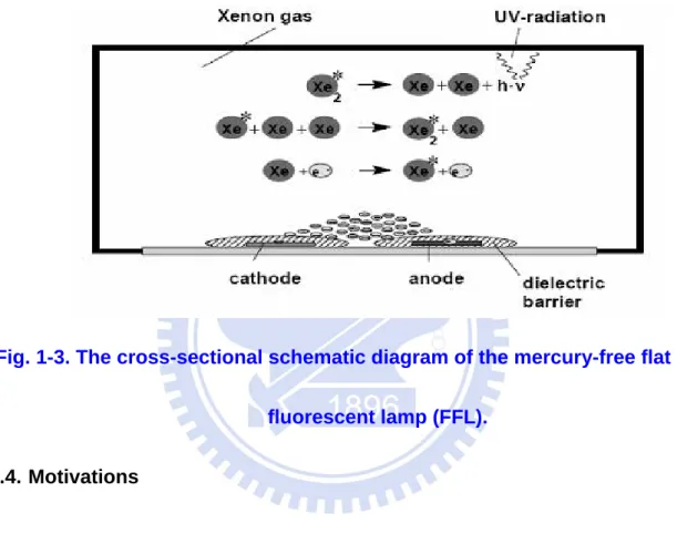
Recently, Flat Fluorescent Lamp (FFL) has provided the other alternative for backlight units using xenon as a discharge gas accompanied with neon as a buffer gas rather than mercury. Fig.1-3 shows the schematic diagram of the flat fluorescent lamp. The parallel electrodes were screen printed on the rear panel and coated with the dielectric layer and phosphor layer, respectively. While applying the voltage, glow discharge would be made and emitted the vacuum ultraviolet (VUV) radiations in the whole discharge volume. VUV
radiations would excite the phosphor layer to radiate visible white light. FFL has realized a thin and flat rectangular lamp to achieve uniform lighting source. However, the luminous efficient is still not high enough and the driving voltage is rather higher than 1~2 kV.
Fig. 1-3. The cross-sectional schematic diagram of the mercury-free flat
fluorescent lamp (FFL).
1.4. Motivations
As the high technology and green technology are progressing rapidly in the recent ten years, the power-saved and environmental protection are going to becoming more and more serious issues according to all kinds of the products in the variety fields. As illustrated above, the common backlights for liquid crystal display or just lighting lamps, for example, are usually filled with the mercury vapor which is provided excellent performance of brightness.
Some mercury-free lamps, liked flat fluorescent lamp (FFL) and light emitted diode (LED), are being developed and investigated recently. However, the driving voltage of mercury-free FFL, filled with inert gas, is further high even more than1~2 kV for the good illumination performance. The cost of LED is still high to apply to the large scale LCD backlight applications.
Based on our previous works on microplasma device [3] ~ [8], the adoption of the nano-tip as an electrode in the panel type device has been ignited the plasma with the lower driving voltage compared with the panel without the nano-tips successfully. It provides the now approaches to be a backlight for liquid crystal display.
In this thesis, we employ the needle like electrode such as the nano-tips and conical electrode to fabricate in the fourteen inch diagonal size glass substrate. With the sharper electrode, the enhanced field is improved locally. Back-filled the research grade of xenon as a discharge gas, the higher vacuum ultraviolet (VUV) is emitted with the low driving voltage due to electron field emission effect. The visible white light is emitted which is converted from VUV radiation by phosphor layer.
1.5. Organization
This thesis is going to mention about “Development of Nano-Tips Electrode Enhanced Plasma Lamp (NTL) for Liquid Crystal Display.” It is structured as follows. A brief concept of mercury-free flat lamp, plasma science, and field emission technology will be described in the Chapter 2. In Chapter 3, the fabrication processes of the proposed flat lamp are provided. Besides, the experimental setup used to operate this flat lamp is presented. In Chapter 4, the collected data including optical appearance, I-V characteristics and luminance and luminous efficiency are discussed and illustrated. We also discuss about the advanced Conical Electrode Enhanced Plasma Lamp (CPL). Finally, the conclusions of this works will be mentioned in the Chapter 5.
Chapter 2
PLASMA THEORY
2.1. Background of the Mercury-free Lamp
So far, cold cathode fluorescent lamps (CCFLs) play an important role not only a daily lighting lamp but also a backlight unit for liquid crystal display (LCD) since the high luminance and mature processes CCFLs achieved. However, the high luminance of CCFLs is coming from the filled mercury vapor inside the tube. As the environmental protection and green technology springs up, the use of mercury for the fluorescent lamp would be restricted further. In order to solve these critical issues, more and more mercury-free lamps are researched and developed as an alternative lamp for the next generation [9]~[23]. The alternative of mercury, however, must provide some properties such as chemically stable, intense vacuum ultraviolet (VUV) radiations and longer VUV radiation wavelength. From these reasons above, xenon (Xe) is the best choice of a discharge gas [9]. In addition, for lower the driving voltage, buffer gases such as helium (He), argon (Ar) and/or neon (Ne) are introduced to collocate for the Penning effect. Therefore, mercury-free plasma flat lamp has
the advantages of extremely long service life, constant luminance over wide temperature range, and mercury-free.
2.1.1 Planon®
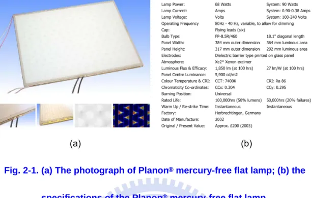
In 2002, OSRAM GmbH proposed a mercury-free flat lamp “Planon®” which is achieved on the 384 mm×317 mm panel [11], [12]. As shown in fig. 2-1 (a), the cathodes and anodes of Planon® were configured as parallel on the rear panel and the cathodes are designed a protrusion pattern toward to anodes so as to shorten the discharge gap and enhance the electric field locally by applied voltage. The inert gas, xenon and neon, is ionized and excited by electron impact reactions to generate the plasma and then emits vacuum ultraviolet (VUV). These VUV is going to stimulate the phosphor to emit the visible white light. The triangular discharge patterns were formed at each protrusion in fig. 2-1 (a). According to the fig. 2-1 (b), Planon® have achieved on 15-30 inch diagonal size panel with 100 torr xenon gas filled, by 1~10 kV driving and realized 5900 cd/m2 of luminance and 27 lm/W of luminous efficiency.
(a) (b)
Fig. 2-1. (a) The photograph of Planon® mercury-free flat lamp; (b) the
specifications of the Planon® mercury-free flat lamp.
2.1.2 Coplanar type mercury-free lamp
In Japan, Prof. Mikoshiba proposed a Xe flat discharge lamp which the coplanar electrodes is configured both sides and separated from 75 mm in fig. 2-2 (a) [13]~[17]. In fig. 2-2 (b), the maximum luminance of 9200 cd/m2 with efficacy of 20.4 lm/W were achieved for 1.3~6.7 kPa of Ar / Xe(28%) gas mixture by pulse width of 2.5 μs and interval of 40 μs on the 5.2 inch diagonal size panel. However, this panel still needed 800~1200 V for the high luminance and luminous efficiency in fig. 2-2 (b) because of long discharge gap.
(a) (b)
Fig. 2-2. (a) The cross-sectional schematic diagram of the coplanar type
mercury-free lamp; (b) the luminance and efficacy of the coplanar type
mercury-free lamp as a function of the applied voltage.
2.1.3 Dual coplanar type mercury-free flat lamp
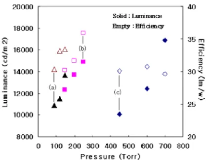
In 2006, a Korean professor Kyung-Cheol Choi from KAIST developed a mercury-free lamp with dual coplanar electrode [22], [23]. Xenon is filled as a discharge gas accompanied with neon as a buffer gas. As we can see in fig. 2-3, the anodes and cathodes are deposited as parallel on the rear panel in order to prolong the gap for gas discharge. The thin electrodes, can be passed by the visible light, is deposited on the front panel as well to enhance the luminous efficiency more. For a dual coplanar lamp, brightness and efficacy
were improved by 80% compared to a conventional coplanar lamp due to the longer gas discharge gap. According to the fig. 2-4, an efficacy of 35.9 lm/w (14900 cd/m2) was achieved for 250 torr of a Xe(30%) / Ne(70%) gas mixture, by a 20-kHz, peak voltage 2.8 kV ac pulse driving. In spite of high luminance and luminous efficiency this panel acquired, it needed to applied 2.8 kV to achieve due to the longer discharge gap. The complex inverter, cost and high risk need to be concerned with high applied voltage.
Fig. 2-3. The cross-sectional schematic diagram of the dual coplanar
Fig. 2-4. Luminance and efficiency of the dual coplanar mercury-free flat
lamp as a function of the gas pressure by a 20-kHz, peak voltage 2.8 kV
of AC pulse driving.
2.2. Gas discharge (Plasma)
2.2.1 Plasma science
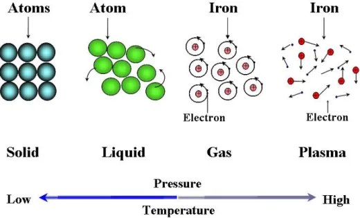
In the following pages, the basic concepts of plasma science would be introduced. The rapid growth of plasma technology is reflected in applications that are today already making our daily lives more convenient and healthier. Plasma is known as fourth state of matter in the universe besides solid, liquid
and gas as shown in the fig. 2-5.
Fig. 2-5. Four kinds of matter states in the universe.
While gas atoms, the uncharged particles were ionized as the temperature raised, the electric properties of these ionized gas were changed. Theoretically, plasma is defined as the ionized gas, made up of equal number free-flowing positively charge ions and negatively charge electrons simultaneously. Plasma would be generated by the collisions between gas atoms and electrons by applying the electric field between both electrodes in the gas environment. Substantially, the energy of plasma is further high, however, plasma is still a quasi-neutral gas of charged and neutral particles which exhibits collective behavior. Plasma would provide some features liked high electric conductivity and electromagnetic. As shown in fig. 2-6, the
in earth, sun, star and magneto in the universe of the nature plasma and display as well as joining and cutting of artificial plasma. Now the plasma is researched to work for the environmental protection of the poisoned recycle. In fig. 2-7, the current-voltage (I-V) characteristic of glow discharge is presented and classified several parts: Townsend discharge, subnormal glow, normal glow, abnormal glow and arc transition.
Fig. 2-7. The current-voltage (I-V) characteristics of glow discharge.
2.2.2 Gas breakdown and reactions
Gas glow discharge reactions are composed of variety kinds of mechanisms and mainly separated into gas volume discharge and cathode surface reaction. The reactions of gas volume discharge are involving ionization, excitation, metastable generation and Penning ionization and spontaneous emission. The reactions including ionization, excitation, three body collision and stepwise ionization will introduce here and spontaneous
emission in next section. Referenced from the gas discharge plasma display panel, the important reactions for discharge in xenon gas are provided below.
1) Ionization by electron
e - + Xe → Xe+ +2 e – (energy=12.1 e.V.) ..(Equa.2-1) 2) Excitation by electron
e - + Xe → Xer* (3P1)+ e – (energy=8.44 e.V.)...(Equa.2-2)
e - + Xe → Xem* (3P2) + e – (energy=8.32 e.V.) ..(Equa.2-3)
3) Three-body collision
Xem* (3P2) + 2 Xe → Xe2* (3Σu) + Xe ...(Equa.2-4)
Xer* (3P1) + 2 Xe → Xe2* (Ou+) + Xe...(Equa. 2-5)
4) Stepwise ionization
e - + Xem* (3P2) → Xe+ +2 e – (energy=3.8 e.V.) ...(Equa.2-6)
e - + Xer* (3P1) → Xe+ +2 e – (energy=3.68 e.V.) ...(Equa.2-7)
Above all, most of the xenon atoms are excited by the electrons impact excitation and promoted from the ground state to high level state of the resonate state of Xer* (3P1) and metastable state of Xem* (3P2) in Equa. 2-2 and
the three-body collisions and generate Xe2* of dimer state in Equa. 2-4 and 2-5.
However, some electron impact deexcitations are provided in Equa. 2-6 and 2-7.
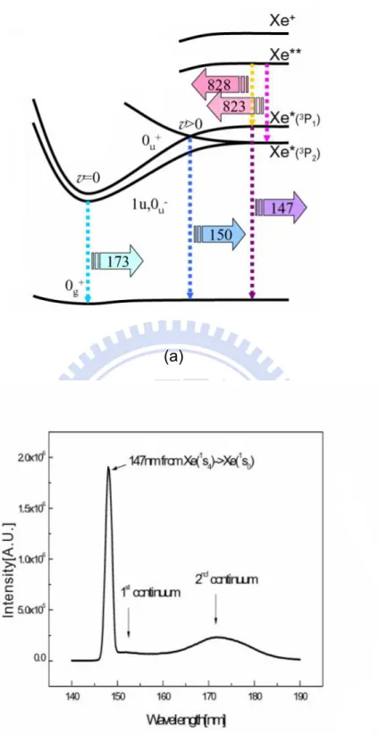
2.2.3 Spontaneous emission of VUV generation
After electron impact excitation and three body collisions, the energy state of the xenon particle has been promoted the higher level. Actually, the mean free path and lifetime of the excited state of xenon is not long. These excited states of the xenon are released to the ground state of the xenon and emit some light. The light emission from xenon discharge is the VUV radiations, the atomic emission (147 nm) from Xer* (3P1) and the first and second continuums
(150 nm and 173 nm) from Xe dimer excited states, and infrared (IR) emissions of 828 and 823 nm, respectively. These reactions are listed below. The diagram of the energy state and emission spectra are depicted in fig.2-8
5) Spontaneous emission
Xer* (3P1) → Xe + hυ(147 nm) ...(Equa.2-8)
Xe2* (3Σu) → 2 Xe + hυ (173 nm) ...(Equa.2-9)
(a)
(b)
Fig. 2-8. (a) The diagram of energy level transition of the xenon gas
discharge reactions; (b) The VUV wavelength intensity of the xenon gas
2.3. Field emission technologies
Field emission effect, came up by Crost, Shoulder and Zinn, is a kind of field-controlled electrons source. The following pages are explained the basic concept of the field emission including quantum tunnel effects and Fowler-Nordheim equation.
2.3.1 Quantum tunnel effect
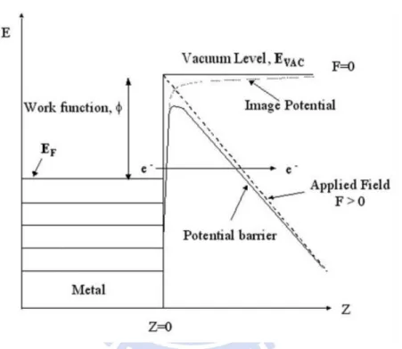
Basically, the theorem of electron field emission from the surface of the metal is a quantum tunneling effect. The fig. 2-9 shows the diagram of the energy level between metal and vacuum while the applied field F=0 and F>0. Under the conditions without applying electric field, the electrons from the metal must need the high enough energy to pass through the potential barrier between metal and vacuum. However, if the sufficient electric field is applied on the surface of the metal, electrons will escape from the conductive solid surface, such as a metal or a semiconductor, and pass through the potential barrier into vacuum. If electric field is extremely high, the distributions of vacuum level on the surface of metal will be converted from the step potential
barrier (F=0) into triangular potential barrier (F>0) which results in a thin potential barrier. Therefore, the possibilities for electrons to pass through the potential barrier will be increased drastically as well as the current. The current of field emission will be characterized in the following pages.
Fig. 2-9. The diagram of energy level and energy density on the surface
of the metal in vacuum while applied field F > 0 and F = 0.
2.3.2 Fowler-Nordheim equation
In other words, the electrons field emission is a kind of cold cathode effect caused by applied field rather than heat. In 1928, R.H.Fowler and W.Nordheim
characterized the Fowler-Nordheim (F-N) equation between field emission current and electric field according to the quantum Schrodinger equation and Schottky effect [24]. F-N equation is described the electrons passed through the potential barrier (Φ, eV) under the electric field (F). The F-N equation is derived 2 3/ 2 2 exp[ ( ) ] ( ) A F I B y t y F α ν Φ = − Φ ………(Equa. 2-11)
where I is the field emission current (A), F: electric field (V/cm), Φ is work function of the metal (eV), A = 1.56×10⁻⁶, B = 6.87×10⁷, y = 3.79×10⁻⁴E1/2Φ-1. For the convenience t2(y) is assumed 1.1 and v(y) is assumed 0.95-y2, equaled approximately 1. According the F-N equation above, if we need the sufficient current, the voltage must be increased on the surface of the metal in vacuum. However, nowadays we work for the application with low driving voltage and lower driving voltage. To solve this problem, the needle like electrode of structure is introduced as an electron emitter. If the electrode becomes as sharper as a needle, there are more charge particles accumulated at the top, namely high electric field with a field enhancement factor (β).
V F d β = ...(Equa.2-12)
function of the material as well as high field enhancement factor of electrode must be concerned for the high intensity of current.
Chapter 3
EXPERIMENT
3.1. Introductions
In the following pages, the fabrication processes of Nano-tips electrode enhanced plasma flat lamp (NTL) would be introduced. A cross-sectional schematic diagram of the proposed plasma flat light source of NTL with the nano-tips enhanced electrodes is presented in the fig. 3-1.
Fig. 3-1. The cross-sectional schematic diagram of the nano-tips
As shown in fig. 3-1, the NTL is consisted of two parts; one is the rear glass panel and the other is front glass panel. The metal electrodes fabricated on the rear panel are consisted of silver electrode layer, deposited by screen printing method, nano-tips electrode, fabricated by semiconductor process, and aluminum rods, which is 2.6 mm in height. The nano-tip structure is showed by scanning electron microscope (SEM) photograph in fig. 3-1. The integrated electrodes on the rear glass panel included silver electrodes layer, aluminum rods and nano-tips electrodes are covered entirely with dielectric layer which the thickness is 40 µm. On the front panel, the indium tin oxide (ITO) electrodes are patterned by the conventional photolithographic techniques and wet etching processes to which can be transparent by the visible light for the human eyes. ITO electrodes patterned on the front panel also are covered by dielectric layer. The dielectric layer upon the both electrodes can avoid from the discharge current increasing abruptly so that generate the stable plasma with lower discharge current. The phosphor which is converted from vacuum ultraviolet (VUV) into visible white light, deposited on the inner surface of both substrate, are 100 µm and 20 µm in thickness on the rear panel and front panel, respectively. All the specifications of the NTL are presented in table 3-1. Two panels are sealed with 2.8 mm height and 5
mm width spacers and frames so as to maintain the effective discharge volume In NTL. After sealing, the NTL is evacuated by high vacuum system which the base vacuum is 10-7 torr and back-filled research grade discharge gas. All the flowchart of the NTL is provided in the fig. 3-2. Besides NTL, the advanced conical electrode enhanced plasma flat lamp (CPL) would be mentioned in the chapter fourth subsequently. The detailed fabrication of each processes are explained in the following sections.
Fig. 3-2. The flowchart of fabricated NTL.
3.2. Fabrication processes
3.2.1. Substrate preparation
The nano-tips electrode enhance plasma flat lamp (NTL) was achieved on the 14 inch diagonal size glass substrate. For the better performance,
therefore, the high distortion point glass (Asahi glass, PD-200) was used as the substrates in front panel and rear panel which the size was 320×300 mm. As shown in fig. 3-3, the surface of glass substrates is cleaned first with isopropyl alcohol (IPA) and acetone (ACE), respectively. To avoid the residual stresses on the glass substrates, both glass substrates used in rear and front panel were adopted pre-annealing processes which suffered the heating treatment, which the highest temperature of the profile is 550℃ for five and half hours, in the furnace.
Fig. 3-3. The glass substrate cleaning before all the processes.
3.2.2. I TO electrode patterning
indium tin oxide (ITO) as the front electrodes on the front panel. In general, the transparent conducting film of the electrode in flat panel display technology is fabricated by sputtering with indium tin oxide target coated upon the substrate. Thus the ITO electrode is patterned by the conventional photolithographic technique and wet etching method on the front panel.
The detailed descriptions of ITO patterning process are listed as follow and the flowchart is provided in fig. 3-3:
1) Clean the 14-in PD-200 glass substrate with ITO electrode by acetone.
2) Tape the photo-resistor (light gray layer) and anti-exposure layer (black layer) on the ITO glass substrate.
3) Exposure the panel by the exposure machine shown in the fig. 3-4.
4) Develop the pattern after exposing by 1% Na2Co3.
5) Detach the anti-exposure layer (black layer).
6) Etch the ITO electrode by 48% KOH (Potassium Hydroxide). 7) Detach the photo-resistor by 5% NaOH (sodium hydroxide). 8) ITO electrode pattern
Fig. 3-4. The flowchart of ITO electrodes patterned on the front panel
of the NTL.
3.2.3. Silver deposition
For the wider plasma phenomenon in NTL, the flat silver electrode is deposited on the rear glass panel. The mainly process of silver electrode deposition is made by silver paste by screen printing method. This method provided merits of the high throughput and low equipment cost but demerits of rougher printed surface. The photograph of screen printing mechanism is shown in fig. 3-6. After initial cleaning of glass substrate, the different mesh of mask would be selected to achieve different thickness. As shown in fig. 3-7, for the better performance of the deposition by screen printing mechanism, the squeegee angle, pressure and speed would be optimized. The printed silver paste would be suffered the soft bake to dry the paste and hard bake to replace the solvent out of the silver paste. The detailed description of the screen printing is provided as follow:
1) Clean the PD-200 glass substrate entirely by acetone and alcohol.
2) Suitable mesh number mask, achieve the different thickness. 3) Print the silver paste, the lot number of silver paste is
PBP019 from DuPont, by the screen printing mechanism. 4) Soft bake the printed sliver paste with 150℃ for ten minutes.
5) Repeat the process 3 and 4 until the available thickness (7μm) of NTL acquired is achieved.
6) Hard bake the panel to replace the solvent of the original silver material with 540 ℃ for five and half hours.
Fig. 3-6. The photograph of the screen thick printing machine of silver
Fig. 3-7. Three main parameters : squeegee angle, pressure and speed,
of the screen printing method.
3.2.4. Dielectric layer deposition
Based on the section 3.2.1 of fabrication, the dielectric layer is used to coat on the both electrode on the rear panel and front panel. The screen printing methods are used to realize the dielectric layer deposition. The function of the dielectric layer upon the both electrodes is used to avoid from the discharge current increasing abruptly and generate the arc discharge instead of the stable plasma. The following is the list of the operations of the dielectric layer deposition:
1) Suitable number mesh mask, achieve the thickness NTL need.
material is PDL-026 from Nippon Electric Glass company, Ltd, by the screen printing mechanism.
3) Soft bake the printed sliver paste with 150℃ for ten minutes. 4) Repeat the process 3 and 4 until the thickness (40μm for the
rear panel and 20μm for the front panel) NTL is achieved. 5) Hard bake the panel to replace the solvent of the original
silver material with 560 oC for five and half hours.
Fig. 3-8. The photograph of the screen thick printing machine of the
3.2.5. Phosphor layer deposition
As we mentioned above, nano-tips electrode enhanced plasma flat lamp (NTL) is using xenon as a discharge gas rather than poisoned mercury. Xenon is the active vacuum ultraviolet (VUV) generating, two main VUV radiations coming from the excited xenon atomic resonance radiation at 147 nm and molecular band centered at 173 nm. These VUV radiation lights of gas discharge are converted to visible white light by phosphor layer.
The mainly process of phosphor layer deposition is made by phosphor paste by spraying method on the rear panel for 100 µm and screen printing method on the front panel for 20μm, respectively. The main component of phosphor paste is distempered by Ca10 (PO4)6FCl: Sb, Mn powder with the vehicle, consisted of high boiling point solvent and binder. On the rear panel of NTL, the spraying method is adopted for rear electrode configuration. The phosphor paste is installed with magnet agitator which is shown in fig. 3-9(a). The nozzle, shown in fig. 3-9(b), is spraying back and forth on the rear panel. The thin film of phosphor paste is deposited and the panel is suffered soft bake with 100℃ for ten minutes by heater. After successive processes to achieve thickness, the hard bake is provided to the panel to eliminate the solvent for
540℃ of highest temperature for five and half hours by furnace.
(a) (b)
Fig. 3-9. The photograph of the phosphor deposition; (a) the
photograph of phosphor paste with magnet agitator; (b) the
photograph of nozzle of the spraying instrument.
3.2.6. Panel assembling
After all different functions of the layers fabrication processes on the front and rear panel, both panels are assembled together with the sealing glass and frit paste. As shown in fig. 3-10, the sealing glass we used is 2.8 mm in height and 5 mm in width. With the dispenser mechanism which shown in fig. 3-11(a), the frit pastes is dispensed by nozzle. And then the front panel and rear panel were assembled by clips in fig. 3-11(b) in the furnace which is suffered the
Fig. 3-10. The photograph of the sealing glass.
(a) (b)
Fig. 3-11. The photograph of the panels assembling; (a) the nozzle to
inject with the frit paste; (b) the panel assembled with clips.
3.2.7. Sintering process
As we mentioned above, the screen printing method is introduced significantly. Due to the thick film deposition of screen printing method for all
the paste we used, the heat treatment mechanism of the furnace would be explained in the following pages. For the easy deposition of all paste, the resin and solvent are adopted to mix with the paste powder. With the furnace, it is provided the temperature profile to remove resin and solvent in the different period. The temperature profile is separated into four parts: heat period, keeping period, annealing period, and cooling period which is shown in fig. 3-12 and 3-13. Heating period is provided to remove the residual solvent, water vapor and dissolute the resin with heat. Keeping period is provided to combine the binder and paste material. In the annealing period, the profile is decreased slowly according to the substrate deformation by temperature. Eventually, the cooling period is provided. The detailed proposal of four profiles is listed as below:
1) Heating period:
¾ Remove the residual solvent and water. ¾ Resin dissolution.
2) Keeping period:
¾ Combine the binder and paste material 3) Annealing period:
¾ Release the substrate deformation. 4) Cooling period:
Fig. 3-12. The schematic diagram of the hard-bake furnace (above)
and temperature profile of the hard-bake furnace (below).
3.3. Experimental setup
3.3.1. High vacuum and gas filled system
After all processes and panel assembly, the NTL is deserved the high vacuum system and back-filled gas system in order to evacuate the gas and fill the inert discharge gas in order. As shown in fig. 3-14, the high vacuum system is consisted of turbo pump, rough rotary pump and gas back-filled system. The base vacuum level of the vacuum system is 10-6 torr. The operations of the vacuum system are explained below.
1) Installation: The panel is connected with the exhaust tube to the chamber of the vacuum system.
2) Rough pumping: Turn on the RV and turn on the S1 until the reading valve of the rough pump gauge is achieved 10-3 torr. 3) Turbo pumping: After 10-3 torr, turn on the RV and turn on the MV
and FV until the reading valve of the high pump gauge is achieved the base vacuum level 10-6 torr.
removing some impurity inside the panel.
5) Research grade gas filled: Turn off the S1, and then back-filled the research grade gas by mass flow controller (MFC) for the stable gas insert.
Fig. 3-14. The high vacuum and gas filled system.
3.3.2. Driving mechanism
Fig. 3-15 (a) shows the photograph of the direct current (DC) pulse bipolar waveform generator (Shen Chang Electric CO Ltd, SPIK 2000A). In fig. 3-15 (b), by changing the different tON+, tOFF-, tON- and tOFF-, we can vary the different
pulse width (τ), pulse interval (Τ) and driving frequency (f). The maximum amplitude of voltages which power supply can be applied is 1 kV as showed in
Table 3-2.
(a) (b)
Fig. 3-15. (a) The photograph of the DC pulse bipolar waveform generator;
(b) the diagram of the waveform of the DC pulse bipolar of the supply.
Table 3-2. The condition of driving mechanism.
Parameter Conditions Waveform Bipolar Frequency 2, 25 and 50 kHz
Amplitude 0-1000 V
3.3.3. BM-7 luminance meter
By applying the DC pulse bipolar waveform to the NTL, the visible white light is emitted from the conversion of VUV radiations by phosphor layer. In order to detect the results of luminance, BM-7 is adopted for luminance
the BM-7, the results of the luminance (cd/m2)、Color temperature (oC) and CIE color coordinates (x,y,z) would be detect.
Chapter 4
Results and discussion
4.1. Nano-tips electrode enhanced plasma flat lamp (NTL)
In this chapter, the experimental results about optical properties and electric characteristics of nano-tips electrode enhanced plasma flat lamp (NTL) will be mentioned. The main idea for nano-tips electrode is to give a needle like field emitter as a rear electrode on the rear panel to emit the electrons from field emission effect. With the dominant electrons, the initial plasma, occurred at the tiny discharge gap firstly, make lower driving voltage and higher VUV radiations. Moreover, because of the high potential differences between the plasma and electrodes, the plasma is going to develop along the ITO electrode and nano-tips electrodes to expand the plasma development into the discharge volume in NTL.
4.1.1 Optical properties
As we mentioned above, the nano-tips electrode enhanced plasma flat lamp has been confirmed on the 14 inch diagonal size glass substrate. In the following pages, the photograph of plasma phenomena in NTL is presented which is taken by conventional digital camera. The rear panel of NTL is composed of three columns of the silver electrode and there are four cells for each which is shown in fig. 3-1. The fig. f-1 demonstrates with the photograph of the NTL while igniting under the conditions of pure xenon gas composition and 50 torr pressure. As you know well, the expanding of plasma results in high potential energy of plasma. Based on the fig. 4-1, therefore, the NTL, in which is filled with 50 torr of the pure xenon gas successfully has provided bright, uniform, and stable plasma in 14 inch diagonal panel as a backlight in liquid crystal display.
Fig. 4-1. The optical appearance of NTL filled with 50 torr, pure xenon gas,
under the frequency 50 kHz, current 0.26 A and voltage 260 V.
4.1.2 I-V characteristics
The breakdown of the glow discharge is defined as a threshold between the non-conductive medium to conductive medium when the sufficient and strong electric field is applied. As we can see in the fig.4-2, it shows the current-voltage (I-V) characteristics of NTL filled with pure xenon in 50 torr pressure. The discharge current of NTL is increased as a function of the applied voltages. In addition, plasma resistance of NTL is positive, which is revealed the NTL is operated in the abnormal glow discharge mode in fig. 2-7.
Fig. 4-2. The I-V characteristic of NTL of the 50 torr pressure and pure
xenon under the 50 kHz frequency of the DC pulse bipolar waveform.
4.1.3 Luminance and luminous efficiency
From optical appearance of NTL under the DC pulse bipolar waveform driving above, NTL has achieved brighter and stable plasma phenomena obviously on 14 inch diagonal glass substrate. By the luminance meter instrument, BM-7 is introduced to detect the luminance results (cd/m2). Luminance is defined as a photometric measure of the density of luminous intensity in a given direction. It describes the amount of light that passes
through or is emitted from a particular area, and falls within a given solid angle. The equation of the luminance is given below:
2 luminance= cos F d A θ ∂ ∂ ∂ ………. (Equa. 4-1) where luminance (cd/m2)
F is the luminous flux or luminous power (lm),
is the angle between the surface normal and the specified direction,
A is the area of the surface (m2), and
is the solid angle (sr).
Based on the efficiency of plasma display panel (PDP), the luminous efficiency (lm/W) is calculated by Equa. 4-2:
luminance area luminous efficiemcy=
I V
π
× ×× ...(Equa.4-2)
Table 4-1. The electric results of the NTL.
Frequency [Hz] Voltage [V] Current [A] Luminance [cd/m2] Efficiency [lm/W] 50 kHz 150 0.10 1250 16.04 50 kHz 180 0.12 1648 14.69 50 kHz 200 0.14 1763 12.12 50 kHz 220 0.16 2054 11.23 50 kHz 240 0.19 2763 11.08
By the luminance measurement from BM-7, the luminance datum is listed in the table 4-1. As shown in fig. 4-3, NTL is achieved 3780 cd/m2 of luminance and 11 lm/W of luminous efficiency respectively under the condition of driving voltages is 260 V, discharge current is 0.26 A and driving frequency is 50 kHz. The luminance of the NTL is improved as a function of the applied voltage. The luminance is enhanced to accompany the improvement of discharge current to provide the electrons to make the lower driving voltage and higher VUV radiations. As calculation of luminous efficiency of NTL from luminance which showed in equation 4-2, the luminous efficiency is also listed in table 4-1. Luminous efficiency of the NTL is decreased because additional power is used to expand the plasma from the sharp nano-tip to more flat electrode. For the comparisons, we also fabricated the panel without the nano-tips. No plasma is ignited even if 1 kV of high driving voltage by DC pulse bipolar waveform. As a result, the concepts with the nano-tips electrode adoption are worked to ignite the plasma significantly with lower the driving voltage in NTL.
Fig. 4-3. The Luminance and luminous efficiency on NTL, filled with 50
torr pure xenon as a function of the applied voltage.
In summaries, the nano-tips enhanced plasma flat lamps (NTL) as a backlight for liquid crystal display is proposed on 14 inch size, and its characteristics as well as optimizations are investigated. As mentioned above, the NTL has been ignited the plasma with low driving voltages less than 300 V using the tiny discharge gap located between nano-tips electrodes and ITO electrodes compared with other conventional backlights. The luminance and luminous efficiency of NTL have achieved 3780 cd/m2 and 11 lm/W under the
conditions of pure xenon gas composition, 50 torr pressure, and 50 kHz, and DC pulse bipolar driving waveform. The fabrication processes of the NTL are kinds of the low cost processes and filled the xenon to be a discharge instead of mercury so as to solve the pollution issue over the world.
4.2. Conical electrode enhanced plasma flat lamp (CPL)
4.2.1. Structure of the CPL
According to the electrical properties and optical appearance of NTL we described above, we suggested NTL as a backlight for liquid crystal display. However, plasma igniting of NTL in fig.4-1 is still not distributed entirely into the whole discharge volume. Furthermore, the luminous efficiency is still not sufficient to act as a backlight or even just a lighting lamp.
Consequently, we suggested an advanced conical electrode enhanced plasma flat lamp (CPL) particularly. The cross-sectional and top-viewed schematic diagrams of CPL are provided in fig. 4-4 and fig. 4-5. CPL is filled with higher VUV radiation intensity of the xenon as a discharge gas compared to other inert gas. As shown in fig. 4-4, sharper conical electrode which the
electrons are coming out is adopted to induce the field emission effect. Base on the concepts of field emission effect we mentioned in chapter 2, the sharper conical electrode is provided the high field enhancement factor, it provides perpendicularly high electric field at the tiny discharge gap between both electrodes in CPL. Also, the local electric field is enhanced more and it makes the higher intense of VUV radiations with lower driving voltage in CPL.
Fig. 4-4. The cross-sectional schematic diagram of conical electrode
Fig. 4-5. The top-viewed schematic diagram of the conical electrode
enhanced plasma flat lamp with 48 cells structure.
The specification of CPL is given in the table 4-2. In the table 4-3, except the new design of conical electrode, thicker dielectric layer and more number of cells is used in CPL.
Table 4-2. The specifications of the advanced conical electrode enhanced
plasma flat lamp (CPL).
Rear Panel Material Specification Front Panel Material Specification
Glass panel PD-200 320x300 mm Glass panel PD-200 320x300 mm
Electrode Silver paste 10 µm Electrode ITO film ~1300 Å
Al conical Aluminum 2.6 mm Dielectric PbO, B2O3, and TiO2 60 µm
Dielectric PbO, B2O3, and TiO2 40 µm Phosphor Ca10(PO4)6FCl:Sb,Mn 20 µm
Phosphor Ca10(PO4)6FCl:Sb,Mn 100 µm Spacer PD-200
5 mm (W) 2.8 mm (H)
Table 4-3. The comparisons of fabrication between NTL and CPL.
Panel NTL CPL
Electrode design Nano-tip and rod electrode Conical electrode
Thickness of dielectric layer 40 µm 60 µm
Numbers of cell 12 48
4.2.2. Optical properties
Fig. 4-6. The optical appearance of the CPL filled with 50 torr, pure
xenon gas, under the frequency 50 kHz, current 0.13 A and voltage
260 V.
As the new structure of the advanced conical electrode enhanced plasma flat lamp is designed, the CPL has been achieved on the 14 inch diagonal size glass substrate. In fig. 4-6, the optical photograph of the
advanced conical electrode enhanced plasma flat lamp is presented. Compared to NTL in chapter 4.1.1, the plasma phenomena of the CPL while igniting under the 260 V of driving voltage is much wider than the NTL. It results from the more numbers of the cell configuration realizing in the CPL. Therefore, more numbers of the cell provide the chances to extend to the applications of the large scale television potentially with easy fabrications.
4.2.3. I-V characteristics
Table 4-4. The electric results of the CPL. Frequency [Hz] Voltage [V] Current [A] Luminance [cd/m2] Efficiency [lm/W] 50 kHz 150 0.08 982 15.75 50 kHz 180 0.09 2547 30.27 50 kHz 200 0.10 3103 29.87 50 kHz 220 0.11 3927 31.24 50 kHz 240 0.12 5532 36.98 50 kHz 260 0.13 7650 43.56
4.2.4. Luminance and luminous efficiency
With the concepts of conical electrode, CPL has ignited the plasma with the lower ignition and sustain voltage below 300 V compared with the conventional plasma lamp due to the tiny discharge gap between the ITO electrode and conical electrodes. Operated in 260 V of driving voltage, CPL has been performed 7650 cd/m2 of luminance and 44 lm/W of luminous
efficiency. As we can see in fig. 4-8, the luminance and luminous efficiency of the CPL is increased as a function of the applied voltage. It means CPL is received high luminance and luminous efficiency at the same driving voltage. In fact, it is totally different compared with other conventional plasma lamp which the luminous efficiency is always decreasing according to the applied voltage. We expect that it results in the electrons from high field enhancement factor of sharper conical electrode.
Fig. 4-8. The luminance and luminous efficiency of the CPL, filled with
50 torr pure xenon as a function of the applied voltage.
4.3. Backlights comparison
To sum up the conventional LCD backlight units nowadays in table 4-5, we compared all the properties of the backlight units. CCFL still has the advantages of the low cost, good color uniformity and good luminous efficiency. The disadvantages, however, of the usage of the mercury is still restricted more according to the environmental protection. The technology of the LED is improving very fast about its properties. LED is realized the excellent luminous efficiency (60-100 lm/W), nice color gamut (>100%) and lower power consumptions. But the heating problems of the circuits and cost problems in
the large-scale panel application are still needed to be concerned. In spite of the fact that FFL solved the mercury-free issue, the high driving voltage and low luminous efficiency must be more advanced as a LCD backlight unit. Therefore, we suggest the advanced CPL with the low cost processes and mercury-free. With the high content xenon and short discharge gap, the CPL is emitted the high luminance visible light and operated in the low driving voltage. We expect the CPL is going to optimize the 100 lm/W of the luminous efficiency.
Chapter 5
Conclusions
According to the progressing the display technologies, more and more excellent and modern products are developing for the convenience of human life. The LCD-TV, for example, provides the thin, light, and power-saved as a home theater display panel. For cost factor and better performance liked high luminance and contrast of LCD panel, lots of the backlight units are investigating and developing recently.
In the work, we have reported two light sources as backlights for LCD panel. NTL with the nano-tips electrode is realized effectively to low driving voltage compared with conventional FFL. The advanced CPL has ignited the plasma with the lower ignition and sustain voltage below 300 V compared with the conventional plasma lamp due to the tiny discharge gap between the indium tin oxide (ITO) electrode and conical electrodes. In particular, while CPL is operated in 260 V of driving voltage, CPL has been performed 7650 cd/m2 of luminance and 44 lm/W of luminous efficiency.
In the future work, the CPL will be optimized the property of the luminous efficiency with the MgO protective layer deposition, which is provided the high secondary electron emission coefficient ( γ ). With the protective layer
deposition, the secondary electrons are emitted by the collisions between the gas atoms and the surface of MgO protective layer and realized the low driving voltage and high intensity of the VUV radiations.