RTUIFR-17
High-Linearity and Temperature-Insensitive 2.4 GHz
SiGe Power
Amplifier with Dynamic-Bias Control
Wei-Chun
Hua', Hung-Hui
Lai',
Po-Tsung
Lin', Chee Wee
Liu'>
* JTzu-Yi Yang', and Gin-Kou
MaZ
Department of
Electrical
Engineering and Graduate
Institute
of Electronics Engineering, National
Taiwan University, Taiwan, R. 0.
C.
*[email protected]
SoC Technology Center, Industrial Technology Research Institute, Taiwan, R.O.C.
2Abstract - A high-linearity and temperature-insensitive
2,4 GHz power amplifier (PA) with dynamic-bias control is
realized in a SiGe HBT technology with 0.9 pm emitter width. Due to the bias linearization, the PldB of 27 dBm is only 0.5
dB smaller than PSsr, which i s the record low to the best of our knowledge. With simple temperature-insensitive bias, the total current deviations from the room temperature are smaller than 6% and 10% at the linear Pa,, (24/20 dBm) for 802.1Ib and 802.11g, respectively at the test temperature from 0 "C to 85 'C. The integrated power detector has a wide dynamic range of 20 dB. The DC current can be reduced to
53 mA and the power-added-efficiency (PAE) can be enhanced up to 3 times at low Pa"* level under dynamic-bias control operation, and meanwhile the 802.11 blg linearity requirements are achieved. This design is most suitable for the future 802.11n application due to its high linearity.
Index Terms - Dynamic-bias control, linearization, power amplifier, temperature-insensitive, and WLAN.
I. INTRODUCTION
There are several WLAN (Wireless Local Area Network) standards operated at 2.4 GHz band, such as lEEE 802.1 1 big and the developing high-throughput standard (802.1 In,
>IO0
Mbps). To have higher throughput in the same bandwidth, spectrum-efficient modulation, such as OFDM, is adopted for 802.1 l g h wireless data transmission. Since the OFDM signal hasv c c vcc
RF In
4
I
I
very high peak to average ratio, the resulting strict linearity requirements on spectral regrowth and error vector magnitude (EVM) make the CMOS PA hard to achieve. In order to lower the cost and to improve the power characteristics, SiGe HBT technology becomes the best candidate for the high-throughput WLAN PA.
There are several techniques to enhance the linearity of the PA, such as predistortion [l], variable feedback [2], and active bias linearization E3
3 .
Among those methods, the active bias linearization shows the greatest enhancement. Therefore, the basic concept of the active bias linearization is adopted in this paper and its performance is fbrther enhanced by adding the temperature-insensitive hnction to operate stably over wide temperature range. The DC power consumption and PAE at low output power level can be improved under dynamic-bias control operation [4].11. DEVICE TECHNOLOGY
The emitter width and length of the unit cell are 0.9
pm
and 20.3 pm, respectively and there are four fingers in a unit cell. In order to ensure the high-power operation, the high-voltage type device is used with a BV,,, of 6 V. The
tneasuredfT. andf,,, of the unit cell are 25 GHz and 32 GHz, respectively. vcc 4 out I
I
t I I Bias Network -,,-,-,-,',,,,,I LFig. 1 Simplified circuit diagram of the power amplifier.
0-7803-8983-2/05/$20.00 Q 2005 IEEE
609
111. CIRCUIT DESIGN
Fig. 1 shows the simplified circuit diagram of the PA. The PA consists of three single-ended common-emitter stages with integrated active bias linearizer and power detector (PD). The inter-stage matching networks are designed partially on-chip while the U 0 matching networks are accomplished off-chip to optimize the PA performances. The inductors with the suffixes of “BW’ are the bond wire inductors. To overcome the low Q on- chip inductor, the high-pass T-matching topology is adopted in the inter-stage matching. The shunt inductors in the inter-stage matching networks can be fulfilled using bond wire inductors and the resulting PA chip is inductor- less. The low-pass output matching network is used to filter out the harmonics.
The collector DC voltages (Vcc) of each stage are fed through quarter-wavelength transmission lines on the FR4 PCB which function as the RF chokes. Various values of the bypass capacitors are placed between the V, node and the ground to filter out wide frequency range of noises.
A . Bias Network
Fig. 2 shows the bias network of the PA. The transistors, Q,. ancl Q.4., act as the current mirror which provides the base bias current of the core transistor (Q,.). The bias current is controlled by the bias control voltage
(VBc)
and R,.. Since the DC voltage of the base node of Q,#is about twice of the base-emitter junction voltage, a diode-connected transistor (Q,) is added to the left branch of the bias circuit to maintain the proper DC level. The linearization mechanism is achieved by the base-emitter junction diode of
0,.
and the bypass capacitor C.,. [3]. The bias linearizer can provide the increase of the base voltage and the collector current of Q.,. as the input power increases. Thus the class-A operating range can be extended to higher input power level to postpone the occurrence of the current waveform clipping and results in higher output P.,dB..The temperature-insensitive function can be achieved by adding resistors in the bias current path, such as RI,,
k.,
and4.
in Fig. 2. The design equation to minimize the base-emitter voltage mismatch between Q,. and Q,. over temperature variation is listed below:where A,(Q,.), A,(Q.J, and
p,
are the emitter area of Q, ,Q.*, and the current gain of Q+, respectively. The resistors in the bias network can reduce (increase) the base-emitter voltages of Q,. and Q, when the bias currentincreases (decreases). As a result, the bias current can be stabilized over wide temperature variation. Since
&.
causes additional power loss and raises the input impedance of the bias network to degrade the linearization mechanism, a bypass capacitor (CJ is added parallel to&.
to maintain the linearization and temperature-insensitive functions simultaneously.R I
T
VBcTVCC
Fig. 2 Linearization and temperature-insensitive bias circuit.
B. Integrated Power Detector Circuit
Fig. 3 shows the integrated power detector circuit of the PA. The transistor Q,. represents the PA transistor of the 3,?-stage. The PD sense the output power level through the collector node of Q.,., the input impedance of the PD should be very high to prevent the power leakage to the PD. The base-emitter-shorted transistor (Q,) is the major part of the PD. The base-collector junction is used since it is more robust than the base-emitter junction due to its lower doping level and thus higher breakdown voltage. When an increasing sinusoidal voltage presents at the output node (collector of Q.,.), the base current of Q,. has an increasing DC level due to the exponential current- voltage relation of a diode (&-V.Bc). The DC current flows from V,,, and then flows through RI., Q, and,
R,
toFig. 3 Integrated power detector with temperature compensation
generate the power detector voltage (VpD). The minimal DC level of the V, can be tailored by the quiescent point of Q,. through the resistive voltage-divider and Q,.. With the base-emitter-shorted transistor (Q,.) at the resistive bias branch, the PD circuit can be less sensitive to the temperature variation.
Iv.
MEASUREMENT RESULTSFig. 4 shows the die photo of the PA. The emitter- grounding inductance is crucial for the single-ended RF PA. Since the Si-based technology has no low-parasitic via-hole process, special treatments such as flip-chip [ 5 ] or heavily-doped sinker [6] are used in the literatures. In this paper, double-bond-wires (at a single pad) are used to minimize the emitter inductive-degeneration effect. Fig. 5 shows the power characteristics of the PA at 2.45 GHz.
The small signal gain, P.ul, and P.,dw are 22.2 dB, 27.5 dBm, and 27 dBm, respectively. The effect of the linearization bias is clearly observed from the gain expansion phenomenon. The maximum linear
P,,,.
that meets the spectrum mask requirements of the 802. I 1 b standard (1 1 Mbps, CCK signal) at 2.45 GHz is 24dBm.Fig. 4 The die photo of the PA (1.48 m m x 0.88 mm).
30 25
5
3
20e
m
8
15 .I 30w
0 25 5 20 n 153
W 10-
;
= %
n A- s
Y -20 -15 -10 -5 0 5 10 15P.
in(dBm)
Fig. 5 The power characteristics of the PA at 2.45 GHz. The small signal gain is 22.2 dB, the P,, i s 27.5 dBm, and the P.,,, is 27 dBm.
The maximum linear Pm, with EVM
of
3.5%, which has better spectrum mask and EVM than the 802.1 l g standard (54 Mbps OFDM signal, 64QAM) is 20dBm. The PAEs at the linear Po", of 24 dBm (1 1 b) and 20 dBm (1 lg)are
12.2% and 7.2%, respectively.
Fig. 6 shows the total current versus power for 0, 25, and 85 "C. The total current variations (AI,,) compared to the total current at 25°C are smaller than 6% and 10% at the linear
Pout
for 802.11b, and g, respectively. The resultingA
I,, is comparable with the commercial 802.11b/g SiGe PA product (e.g. SE2529L of SiGe semiconductor Inc., ~AIc,-l < 10% from -40°C to 85 "C).n 900
4
E
800E
700E
600 30
5003
400 0 l- 30Q Y-
?5 16 17 18 19 20 21 2223
24 25Po, ( d m
Fig. 6 The total current of the PA versus output power for
different temperatures. The A lCC comparisons are based on the data measured at 25°C.
Fig. 7 shows the diagram of V,, versus
Paul
for different temperatures. The variationof
the V,, (0 PC to 85 "C) is smaller than 0.1 V. The dynamic range of the PD is -20 dB (5-25 dBm).Fig. 8 shows the gain and the DC bias current versus bias control voltage (VnC). The tuning range of the V,, is 1 V with the gain slope of -13.5 dBN. The DC bias current can be as low as 53 mA when V,, is set to 1.4 V.
1.8 I
1.6
n
over all
power range
-
.CI 1,4 0>
1.2 W,
E
1.0 0.8 0 5 10 15 20 25P
outIdem)
Fig. 7 The power detector voltage (Vp,) versus output power
for different temperatures.
25
c
Supply Voltage (V) Y 3.3 1 . 1 * 1 m 1 . 1 . 1 . 1 1.4 1.6 1.8 2.0 2.2 2.4 2.6 DC Bias Current (mA) Gain (dB)Fig. 8 The gain and the DC bias current versus the bias control voltage
Fig. 9 shows the PAE and the EVM versus Pout under fixed-bias and dynamic-bias operations. At low Po,, the DC current is reduced, and meanwhile the linearity requirements of 802.1 1 big standards are achieved. When the needed
Po,,
is lower than 20 dBm, the bias current is adjusted to the minimum value that satisfies the spectrum mask and the EVM (< 3.5%) requirements of 802.1lg. Since the PA related linearity requirements of the 802.1 I b standard is looser than those of the 802.1 ig standard, the resulting PA can also work for the 802.1 l b application. ThePAE
at8
dBin Po,, can be enhanced up to 3 times under dynamic-bias operation. Once the optimum bias for each P, is determined, the control mechanism can be realized in the baseband chip to give proper V.BC. according to the desired P,,,. The PA performances are summarized in table I. 14 12 lom
8 s
6 - 4 - 2 0s
8 10 12 14 16 18 20 22 24P”.*
WBm)
Fig. 9 The PAE and EVM performances versus P,,. for dynamic-bias and fixed-bias operations.
180 ; 53* 22.2
v.
CONCLUSIONSA high-linearity and temperature-insensitive SiGe PA for 802.1 I blg WLAN applications is demonstrated in this paper, and which is also promising for the hture high- throughput 802.1 1 n application due to its high linearity. The simple temperature-insensitive bias can provide
~
EVM @ 20 dBm (%) 3.5%
5-25 Power Detector Dynamic
.
Range (dBm)-.
comparable temperature stability as the commercial SiGe PA product. The dynamic-bias control mechanism can dramatically reduce the bias current and enhance the PAE at low P,,, level
to
achievelow
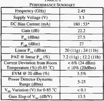
DC power consumption and high linear P,,, simultaneously.TABLE I
PERFORMANCF. SI MMARY
I
Frequency (GHz)I
2 . 4 5-1
I
P.,,, (dBm)I
27 ~~1
Linear P.””, (dBm)
PAE @ linear Pout (%) Current Deviation from Room
Tem erature (%) (0-85 “ C ) 20 ( l l g ) ; 24 ( l l b ) 7.2 (1 Ig) ; 12.2 ( l l b )
<
6% (24 dBm)<
10% (20dBm) < 0.1I
I
V.-,, Variation (V) for 0-8.5 PCI
I
Gain Slop of V,, ( d B N j1
13.5I
*Dynamic-bias operation REFERENCES[ I ] N. Gupta, A. Tombak, and A. Mortazawa, “A Varactor Diode Based Predistortion Circuit,” 2004 IEEE MTT-S Inr. Microwave Symp. Dig., vol. 2, pp. 689-692, June 2004.
[Z] K. Fujita, K. Shirakawa, N. Takahashi, Y. Liu, T. Oks, M.
Yamashita, K. Sakuno, H. Kawamura, M. Hasegawa, H.
Koh, K. Kagoshima, €3. Kijima, and H. Sato, “A 5GHz
High Efficiency and Low Distortion InGaPIGaAs HBT Power Amplifier MMIC,” 2003 IEEE M ? T S Int. Microwave Symp. Dig., vol. 2, pp. 871-874, June 2003.
[3] Y. S. Noh and C. S. Park, “PCSN-CDMA Dual-Band
MMIC Power Amplifier with a Newly Proposed Linearization Bias Circuit,” IEEE J . Solid-State Circuits,
vol. 37,110.9, pp. 1096-1099, Sept. 2002.
Y. -W. Kim, K. -C. Han, S.-Y. Hong, and J. - H. Shin, “A
45% PAE/lXmA Quiescent Current CDMA PAM with a Dynamic Bias Control Circuit,” 2004 IEEE Rudio Frequency Integrated circuits Symp. Dig., pp. 365-368. [5] W. Bischof, M. Alles, S. Gerlach, A. Kruck, A. Schiippen, J.
Sinderhauf, and H. -J. Wassener, “SiGe-Power Amplifiers
in Flipchip and Packaged Technology,” 2001 IEEE Radio Frequency Integrated Circuits Symp. Dig., pp. 35-38.
W, 3akalski, K. Kitlinski, G . Doing, B. Kapfelsperger, W. Osterreicher, W. Auchter, R. Weigel, and A. L. Scholtz, “A
5.25 GHz SiGe Bipolar Power Amplifier for IEEE 802.11a Wireless LAN,” 2004 lEEE Radio Frequency Integrated Circuits Symp. Dig., pp. 567-570.
[4]
[6]