Liquid Crystal Lens Array for 3D Endoscope Application
Amir Hassanfiroozi
a*, Tai-Hsiang Jen
a, Yi-Pai Huang
a, Han-Ping D. Shieh
aa
Department of Photonics and the Institute of Electro-Optical Engineering/Display
Institute, National Chiao Tung University, 30010 Hsinchu, Taiwan
ABSTRACT
A plano-convex electrode is presented for a liquid crystal lens array with a hexagonal arrangement, small inactive region, 30μm cell gap and low applying voltage. It uses circular curved electrodes to provide a smooth, controllable applied potential profile across the aperture to manage the phase profile.
Keywords: Liquid crystal lens, circularly curved electrode, 3D endoscope.
1. INTRODUCTION
On the basis of unique electro-optical characteristics, the material of liquid crystals (LCs) is usually used to study and fabricate some optical devices for applications. Recently, studies of LC lenses have become a popular topic because its capabilities are obviously different from the conventional glass lenses. Until now, numerous types of LC lenses have been proposed such as 3D sensing system 1, Three-dimensional imaging system2 and Optical tunable liquid crystal lens3-5
etc. Also various challenges to make a better liquid crystal lens are demonstrated as photo-polymerized liquid crystal lenses with high applying voltage 6 either complicated structure but good focusing property 7 even a method is developed
to reduce the distortion in the optical system based on liquid crystal lens array for 200 μm aperture size which is impossible to extract three-dimensional image 8 liquid crystal lens with low applying voltage 9-10 stripe-like lenticular
liquid crystal lens11-13 liquid lens actuated by liquid crystal pistons14. Since liquid crystal lenses are thin, tunable in focus
and electrically switchable to 2D/3D modes, it seems it is a good candidate to be used in endoscope to enhance endoscope imaging system whereas endoscopes usually have a solid lens with few millimeter diameters. This is why we are interested to present a small lens based on liquid crystal lens array. In this paper we demonstrated a liquid crystal lens array with a hexagonal arrangement, small inactive region, low applying voltage, and better image quality since it shares the image with 7 lenses instead of 9 lenses in a commonly used arrangement of 3 by 3 lenses. Also unlike to the prior arts we do not use patterned electrode as a lens itself rather we took advantage of this special electrode pattern to achieve a better electric field distribution.
2. EXPERIMENTS
2. 1 Electrode Fabrication Process
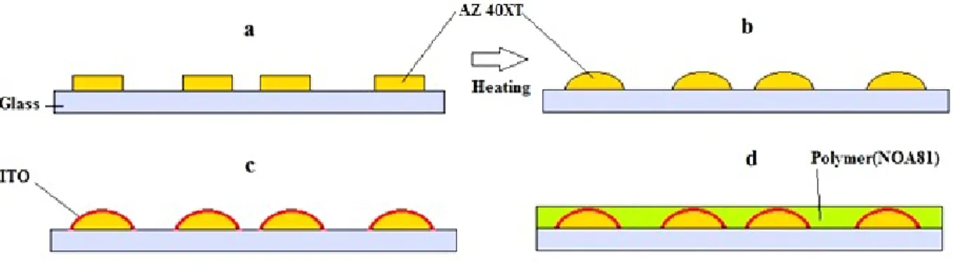
The fabrication processes and the operating principles of our LC lens array are schematically illustrated in Figure 1. As shown in Figure 1(a), our LC lens array has a glass substrate with etched photoresist layers, AZ 40XT is coated with spin coating machine (2000 rpm for 25 seconds). The softbake should take place gradually, 5 minutes at 60˚C and 5 minutes at 80˚C for the applied thickness and this is to avoid bubbles in the resist film during softbake and finally 7 minutes at 130 ˚C to reach to its softening point, it gives photo resist a curved shape. Figure 1(b). The conductive polymer ITO which has a good optical performance is coated, Figure 1(c). Then the UV-curable adhesive NOA81 as a photosensitive prepolymer is coated, we polymerized this layer using a UV light in order to make it solidified as it is depicted in Figure 1(d).
*[email protected]; phone 886-3-5712121#59210; fax 886-3-5737681 Invited Paper
Three-Dimensional Imaging, Visualization, and Display 2014, edited by Bahram Javidi, Jung-Young Son, Osamu Matoba, Manuel Martínez-Corral, Adrian Stern, Proc. of SPIE Vol. 9117, 91170E
© 2014 SPIE · CCC code: 0277-786X/14/$18 · doi: 10.1117/12.2054429 Proc. of SPIE Vol. 9117 91170E-1
a
I-1
l-1
l
Glass -I-ITO I 1 :1Z40 Heating b d Pol}mer(\OA81) 1aQaaaac:=Dc=:)ac:=DQac:=::,
aaaac=:3c="c=Dc=).::=2)c=:)c=)c)a
(=DC)c=pc=2,c7ac=2).:=)c=pc=pc=pc=pc=D
Glass
Z 40XT
ITO
NO Á81 ` -PVLC
PV AITO
_
Glass
Figure 1. Fabrication process of curved circular electrode
2. 2 Device structure
The structure of the LC lens consists of two layers of indium tin oxide (ITO) as electrodes, two glass substrates of thickness 550 μm, a layer of NOA81 (Norland Optical Adhesive) with thickness of 35 μm as an insulating layer, a LC layer with cell gap of 30 μm using ball spacer and two alignment layers of PVA (Polyvinylalcohol) which are mechanically buffed to align LC directors. The rubbing directions of two alignment layers are anti-parallel and the lens diameter for each one is 350 μm. The schema of electrodes is depicted in figure.2 and the LC cell is shown in figure.3.
Figure 2. Indium Tin Oxide on the curved surface of photo-resist
Figure 3. Illustration of the LC lens arrays
The device was filled with nematic liquid crystal material E7 (Merck) with the following properties: dielectric constants 0 . 19 = p ε =5.2 s
ε (Δn=0.225) and liquid crystal effective dielectric constant =9.74 lc
ε . The thickness of liquid
Proc. of SPIE Vol. 9117 91170E-2
CCD P.2 Endoscope Stop kLASER LC lens L4mm
,
crystal layer and glass respectively are =30lc
d μm; dg =550μm, =7.75 g
ε ; the dielectric constant of NOA81 is 5
~ ins
ε at frequency of 1 kHz and the thickness of insulator is =35 ins
d μm. Measurement of the lens properties
3. LENS PERFOMANCE
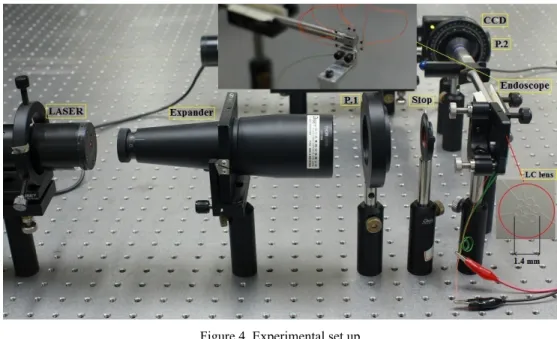
The focusing properties of the LC lens, the image quality, interference patterns, and focal length under different applied voltages were measured. The scheme of the measurement system was set up to probe the voltage-dependent focal length of the LC lens, as shown in figure.4.
Figure 4. Experimental set up
When a voltage (V) is applied to the electrodes, the LC layer experiences an inhomogeneous electric field because the top ITO electrode has spherical shape. Within the LC layer, the electric field at the border
b E and center c E can be calculated as follows: ) ( ins ins lc lc lc b d d V E ε ε ε + = (1) lc c d V E = (2)
We substituted these values above into the equations (1) and (2) we have Ec = 33.33V andEb =10.18V . Whereas
electricfield at the border is less than the center and in addition electric field between two electrodes is superposition of the ring`s electric field at border which can avoid degrading the gradient form of refractive index from center of lens to the border of electrode also over flow of electric field in the center of lens since the lens aperture is too small, the result is clear in figure.5 the electric field at border is less than electric field at center. Also these kinds of electrodes make it possible to work on a wider range of applied voltages, which gives more precise control over focusing as it illustrated in figure.6.
Proc. of SPIE Vol. 9117 91170E-3
200 180 160 E 140 E 5: 120
li
100 V 80 C.1 Nw 60
2 4 6 Voltage, V rms 8 10 25 206
g
141
qh-- -Q
__GI, .,
_fa i
0 0 1 2 3 4 O Voltage, V rms 5 6 7Figure 5. Electric field VS. Voltage at the electrode border and electrode center
Based on the measured interference fringes at different voltages, the focal length of the lens cell can be calculated using the equation
f
lc(
V
)
=
π
D
2/
4
λ
Δ
δ
, where D is aperture width of the lens, λ is the wavelength of incident laser beam, andΔ
δ
is the phase difference between the center part and the border part of the aperture in the interference patterns 4.Figure 6. The focal length of the LC lens as a function of the applied voltage (f = 1kHz).
The total focal length
f
(V
)
of the LC lens can then be expressed as following, wheref
ins(V
)
is the fixed focal length of the Insulating layer (NAO81).) ( 1 ) ( 1 ) ( 1 V f V f V f lc ins + = (3)
Proc. of SPIE Vol. 9117 91170E-4
[um] [um] 32.00 32.00 T}
+i
a...
25.00 20.00 1502 10.03 5.00 0.0099
9+ f I 1 1ff9 T 1 1f}} TT1 1117 1111111 1177 rT1 1 111117 111177 T 111 77711111111 777Ti
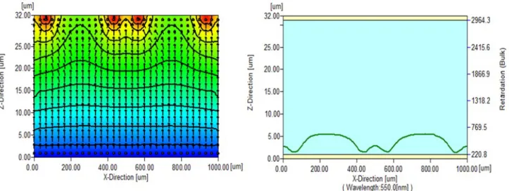
T1 11111 11 711 1111171 1111117 TT 111111111111111111111T7Tii TT117 1111111111117 7777T i111111111111111111 1111111111 1111111111111111111111111 11111111111111111171111111111 11111111111111111111111111111 11111111111111111111111111111 rrrASrIMILKirir&KrIWirLrILILLILrAr 0.00 200.00 400.00 600 00 X-Direction [um] 800.00 1000.00 [um] 25.00 20.00 15.00 10.00 5.00 0.00 0.00 200.00 400.00 600.00 800.00 X-Direction [um] ( Wavelength.550.0[nm] ] 2964.3 2415.6 1866.9 1318.2 769.5 220.8 1000.00 [um]Figure.6 shows the transient properties of the relative phase retardation in a cross-section of our lens arrays. The phase retardation was changed when liquid crystals were rotated by applying the voltage to the curved circular electrodes. Phase retardation of a LC lens is given by:
λ π δ n lc d Δ = 2 (4)
Where
λ
is the wavelength,Δn=0.225,
=30 lcd μm and
λ
= 632 nm. Therefore the maximum phase difference is πδ =10
Δ which means we are supposed to see 10 rings.
Figure 7. Liquid crystal directors direction (left), phase retardation in X-Z section (right)
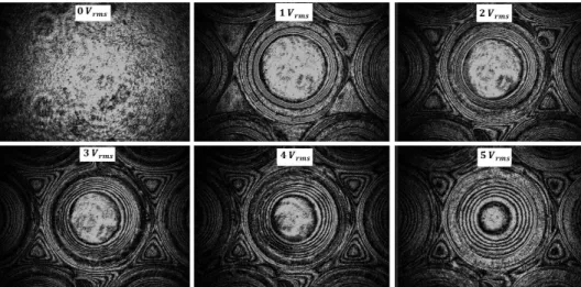
To evaluate the optical properties of this hexagonal LC lens array, the interference fringes between the ordinary and extraordinary rays using a He-Ne laser beam (λ = 632 nm) passed through the lens placed between two crossed polarizers. Figure 8 shows the recorded interference fringes at various applied voltages. When the voltage is applied, the appearance of the interference fringes is changed due to the reorientation of the LC directors which causes by the applied electric field. Note that the retardation difference of two adjacent constructive or destructive interference rings indicates a phase change of 2π. The variation in phase retardation induced by the applied voltage represents how the electrical field alters the lens properties. The curvature of the phase profile of this LC lens array gradually boosts as voltage increases. In addition, the interference patterns are composed of almost circular fringes, it is because of disclination , however circularly hole-patterned electrode possesses some characteristics including easy fabrication, excellent capabilities of tunable focal lengths and large effective apertures etc, but this kind of LC lenses also has a serious drawback, that is, occurrence of disclination lines when operating. It can be solved by adding an extra in-plane electric field in LC lenses, photopolymerization and so on.
Proc. of SPIE Vol. 9117 91170E-5
N
N
Ill Ill lll its N1
s
.
+r
'
it
Figure 8. The interference patterns in LC lenses for applied voltages 0-5 volts.
Moreover, the imaging properties of this LC lens using a side view type endoscope were investigated when the LC lens was placed at a distance of 2 mm from objective lens of endoscope and a photograph (20 mm* 30 mm) at 57 mm far away from the LC lens. The images are taken in dim light as shown in figure 9. Since we are using seven lenses just we need a computer method based on image processing in order to take a photo of the subject in different angles to make a three-dimensional photo of the subjects. Most important benefits from a 3D image capturing research in medical imaging are expected such as more evidence-based decision, better understanding of the effect of treatments on diseases, minimize damage to healthy tissue by targeting the treatment area, more rapid and accurate diagnosis and serve as an easy-to-read visuals for patient education and physicians.
Figure 9. The image focusing/defocusing of the LC lens at (a) Vrms = 4, (b) Vrms = 3 and (c) Vrms = 2 volts.
4. CONCLUSION
We proposed a new liquid crystal lens array using curved circular electrodes and hexagonal arrangement. As the applied voltage varies, focal length could be continuously changed. Due to its small cell gap, fast response time is achievable. The proposed method is more suitable for making LC lenses or lens arrays of a very small size, from several tens to several hundreds of micrometers in diameter. Also it is easy to fabricate and would be very attractive for a wide range of applications that require a miniaturized lens structure and in term of future clinical applications this concept in this paper can also be applied to endoscopes and cameras in cell phones.
REFERENCES
[1] Yi-Pai Huang, Chih-Wei Chen, Myungjin Cho, Bahram Javidi, “Liquid crystal lens for axially distributed three-dimensional sensing,”, Proceedings of SPIE, 8738-4, (2013).
Proc. of SPIE Vol. 9117 91170E-6
[2] Kawamura et al.,“Three-dimensional imaging system by using a liquid crystal lens”,Proceedings of iSOT'J 2, 2012.
[3] Liwei Li, Doug Bryant, Tony Van Heugten, Philip J. Bos , “ Near-diffraction-limited and low-haze electrooptical tunable liquid crystal lens with floating electrodes,” Opt. Express 21(7), 8371-8381(2013).
[4] Hung-Chun Lin, Yi-Hsin Lin, “An electrically tunable-focusing liquid crystal lens with a low voltage and simple electrodes,” Opt. Express 20(3), 2045-2052 (2012).
[5] Mao Ye, Bin Wang, Masaru Uchida, Satoshi Yanase, Shingo Takahashi, and Susumu Sato, “Focus tuning by liquid crystal lens in imaging system,” Jpn. J. Appl. Phys. 51, 7630-7635 (2012).
[6] Che Ju Hsu, Chia Rong Sheu, “Using photopolymerization to achieve tunable liquid crystal lenses with coaxial bifocals,” Opt. Express 20(4), 4738-4746 (2012).
[7] Chao et al.,“A New Negative Liquid Crystal Lens With Multiple Ring Electrodes in Unequal Widths”,IEEE Photonics Journal, vol. 4,No. 1 pp. 250-266, Feb.2012.
[8] Chia-Ting Hsieh, Yu-Feng Hsu, Chia-Wei Chung, Ming-Fei Chen, Wei-Chia Su, Chi-Yen Huang , “ Distortion aberration correction device fabricated with liquid crystal lens array,” Opt. Express 21(2), 1937-1943(2013). [9] Giichi Shibuya, Nobuyuki Okuzawa, Mitsuo Hayashi, “New application of liquid crystal lens of active
polarized filter for micro camera,” Opt. Express 20(25), 27520-27529(2012).
[10] Harry Milton, Paul Brimicombe, Philip Morgan, Helen Gleeson, John Clamp, “Optimization of refractive liquid crystal lenses using an efficient multigrid simulation,” Opt. Express 20(10), 11159-11165(2012).
[11] Kyong Chan Heo, Seung Hun Yu, Jin Hyuk Kwon, and Jin Seog Gwag , “Thermally tunable-focus lenticular lens using liquid crystal,” App. Optics 52(35), 8460-8464, (2013).
[12] Xu et al., “Liquid crystal micro-lenticular array assembled by a fringing field,” J. Appl. Phys. 111, 063104 (2012).
[13] Liang and Wang, “Thermally tunable-focus lenticular lens using liquid crystal,” Journal of Display Technology, vol.9, no. 10, pp.814-818, Oct.2013.
[14] Su Xu, Hongwen Ren, Shin-Tson Wu , “ Adaptive liquid lens actuated by liquid crystal pistons,” Opt. Express 20(27), 28518-28523(2012).
Proc. of SPIE Vol. 9117 91170E-7