國立交通大學
電子工程學系 電子研究所碩士班
碩士論文
一種具有懸浮奈米線通道之新式元件的研製
與分析
Fabrication and Characterization of a Novel Device with
Suspended Nanowire Channels
研 究 生:李冠樟
指導教授:林鴻志 博士
黃調元 博士
一種具有懸浮奈米線通道之新式元件的研製與分析
Fabrication and Characterization of a Novel Device with
Suspended Nanowire Channels
研 究 生:李冠樟 Student: Guan-Jang Li 指導教授:林鴻志 博士 Advisors: Dr. Horng-Chih Lin 黃調元 博士 Dr. Tiao-Yuan Huang
國立交通大學
電子工程學系 電子研究所碩士班
碩士論文
A Thesis
Submitted to Department of Electronics Engineering & Institute of Electronics College of Electrical and Computer Engineering
National Chiao-Tung University in Partial Fulfillment of the Requirements
for the Degree of Master in
Electronic Engineering August 2009
Hsinchu, Taiwan, Republic of China
一種具有懸浮奈米線通道之新式元件的研製與分析
研 究 生:李冠樟 指導教授:林鴻志 博士 黃調元 博士國立交通大學
電子工程學系 電子研究所碩士班
摘要
在本篇論文中,我們成功的製作出具有側閘極以及懸浮奈米線通道結構之新 穎元件。利用邊襯蝕刻技術(sidewall spacer etching technique)以形成奈米線,同時,以去除犧牲氧化層之方式形成空氣介電層並使奈米線通道懸浮。因空氣介電 層的存在,我們可利用調變閘極電壓使奈米線通道受靜電力吸引而擺動。同時, 懸浮奈米線通道元件展現了較小的次臨界擺幅(相較於未去除犧牲氧化層之元 件),以及有趣的振盪現象。在本篇論文中,首次發表藉由奈米線通道擺動所引 發之遲滯(hysteresis)現象。儘管大部份的元件未展現出非常陡峭的轉換特性(次臨 界擺幅低於60mV/dec),我們提出一漸進式吸引模型以解釋此一現象。
Fabrication and Characterization of a Novel Device with
Suspended Nanowire Channels
Student: Guan-Jang Li Advisors: Dr. Horng-Chih Lin Dr. Tiao-Yuan Huang
Department of Electronics Engineering and Institute of Electronics National Chiao Tung University, Hsinchu, Taiwan
Abstract
In this thesis, a novel device featuring a side-gate and suspended nanowire
(NW) channels is proposed and demonstrated. The nanwire channels are formed with
sidewall spacer etching technique, and become suspended by stripping the sacrificial
oxide layer between the gate nitride and nanowire channels. The presence of air gap
leads to a movable channel controlled by the gate bias. Despite a much larger
equivalent oxide thickness due to the air gap, the suspended nanowire channel devices
depict a better subthreshold swing over the devices without stripping the sacrificial
oxide (i.e., no air gap). Moreover, an interesting oscillation phenomenon of suspended
nanowire during the device operation is observed. The hysteresis phenomenon in the
subthreshold characteristics due to the motion of the suspended nanowire is reported,
do not show an abrupt turn-on behavior (i.e., with S.S. < 60mV/dec). A model
considering the gradual contact of NW channel with the gate nitride is proposed to
Acknowledgement
在短暫的碩班生涯中,很高興能加入 ADTL 學習。首先衷心的感謝林鴻志 教授與黃調元教授的指導,在研究的過程中提供我們充分的資源與自由發揮的空 間,以及教導我們研究應有的態度。 不論在研究或學業上,受到很多學長及同學的幫助。感謝蘇俊榮學長在臨 出國之際,仍帶著我們在無塵室進出,在實驗流程及觀念上的建立上給予很大的 幫助。感謝博班的學長盧景森、徐行徽、張凱翔、林哲民、蔡子儀在學業上以及 實驗上的幫助。也要感謝在 NDL 任職的李耀仁學長,在研究的過程中給予我很大 幫助。 同時,在碩班生涯中也認識一群好朋友,洪文強、洪政雄、陳威臣、林漢 仲、江忠祐、劉大偉、陳玲。大家一起熬夜作實驗、一起在球場上盡情的打球, 一起出遊、一起到處吃喝玩樂的那段時光,是我在碩班生涯最珍貴的時光。很高 興能認識你們這群好朋友。 還有學弟妹們,林政頤、郭嘉豪、陳政建、謝瑞桀、張育嘉、戴君帆、張佑 寧、黃瑄勻、張格綸、施維濤、以及眾多碩一學弟妹們,有了你們加入 ADTL 大 家庭,為實驗室帶注入更多的活力,也帶來更多的歡笑聲。 最後,要感謝是我的家人,在我成長的路上一路伴隨著我,父親李豐富先生、 母親凃素貞女士、弟弟李冠億,你們的支持,給予我前進的動力,謝謝你們。 李冠樟 謹誌於 風城交大 2009 年 8 月Contents
Abstract (Chinese)………...……….…I Abstract (English)………...II Acknowledgement………..IV Contents…....……….……...V Table Captions……….………….VII Figure Captions………..………VIII Chapter 1 Introduction1-1 Overview of Nanowire Technology………...1
1-2 Low Subthreshold Swing Devices..………...3
1-2-1 Impact-Ionization MOS (I-MOS)………...4
1-2-2 Tunneling FET (T-FET)...………...5
1-2-3 Suspended Gate MOSFET (SG-MOSFET).………...6
1-3 Motivation………..7
1-4 Organization of This Thesis………...8
Chapter 2 Device Fabrication 2-1 Device Structure and Process Flow………9
2-2 Measurement Setup and Electrical Characterization………11
Chapter 3 Results and Discussion
3-1 Leakage Current and Mechanisms..………...……..13
3-2 Basic Transfer Characteristics...15
3-3 Hysteresis Phenomenon...18
3-3-1 Characteristics of Hysteresis...18
3-3-2 Hysteresis Mechanism...21
3-4 The Suspended NW Channel TFTs with Larger Air Gap………...…….23
Chapter 4 Conclusion and Future Work 4-1 Conclusion….……….……..…….25
4-2 Future Work...……….……..…….26
References……….….…..…...27
Tables.……….….……...32
Table Captions
Table 3-1 Comparisons of suspended NW channel devices with different air gap thickness………...……….……32 Table 3-2 Comparisons of suspended NW devices with different over etch time (with
4.5 nm air gap thickness and 0.4 m channel length) …..………....……32 Table 3-3 Comparisons of suspended NW devices with different over etch time (with
25.5 nm air gap thickness and 1 m channel length) ………...…..……33 Table 3-4 Comparisons of suspended NW channel devices with different air gap
Figure Captions
Chapter 1
Fig.1-1(a) Schematic views of basic device structure of n-channel I-MOS and the band diagrams of the ON \ OFF state……….………35 Fig.1-1(b) a) An electron arrives at the edge of the strong field region at random time τ1. b) The carrier starts impact ionization and avalanche, thereby generating more carriers. However, the multiplication process with fewer carriers is strongly fluctuating and random, until the number of carrier reaches a reasonable amount (about 50) and overcome the randomness in multiplication process. c) The multiplication process continues until the device is fully turned on………36 Fig.1-1(c) In order to achieve a reliable circuit operation, failure rate less than 1ppm
while the device is on is essential (which means only one failure every million operations). For conventional CMOS, the intrinsic delay of 1ppm operation is just a few picosenconds (or less than one). However, with off-state level of 1 μA/μm, I-MOS needs 10 picoseconds for a 1ppm operation. In the trade off between on/off current ratio and dynamic operation delay, I-MOS does not show advantage over conventional CMOS………36 Fig.1-2(a) Schematic view of T-FET device structure. (b) Band diagram under the
on-state, the band diagram in the channel is pulled downward when a proper positive voltage is applied to the gate, hence the barrier is small enough to generate tunneling current. (c) Under the off state, the
reverse-biased P-I-N diode provides a large barrier between source and drain, result in a small off current...…..……….37 Fig.1-3(a) Bird’s view of a SG-MOSFET. The gate is suspended with anchors at both
ends. (b) The mobile gate is controlled by two forces; one is the electrostatic force, and the other is elastic force. (c)Before the Vg reaches Vpi, the electrostatic force is balanced by the elastic force. (d)Once the Vg reaches Vpi, the electrostatic force overcomes the elastic force, and the gate is pulled down toward the gate oxide……….38
Chapter 2
Fig.2-1(a) Schematic view of the NW device. (b) Cross-sectional view of the NW channels and the gate………...…...39 Fig.2-2(a) Si substrate capped with buried oxide in Bird’s view and cross-sectional
view, respectively………...40 Fig.2-2(b) Gate deposition and definition in Bird’s view and cross-sectional view,
respectively……….41 Fig.2-2(c) Gate dielectric and sacrificial layer depositions in Bird’s view and
cross-sectional view, respectively...………..……….…………..…...42 Fig.2-2(d) Amorphous Si deposition and SPC. …………...………...…….…..….….43 Fig.2-2(e) S/D implantation with an energy of 10 keV and a dose of 5x1015 cm-2..……….….44 Fig.2-2(f) S/D and NW channels defined by a dry etch step.…...45 Fig.2-2(g) Using a wet etch step to remove the sacrificial layer to achieve the NW
channels suspension...46 Fig.2-3 SEM image of a fabricated device with suspended NW channels………...47
Fig.2-4 The configuration of the measurement setting, which including a HP 4156A semiconductor parameter analyzer and an AglientTM 5250A switch...47
Chapter 3
Fig.3-1 Schematic of possible paths for off-state leakage currents...48 Fig.3-2 Leakage mechanisms in drain/channel junction. (a) Thermal emission.
(b) Thermionic field emission. (c) Band-to-band tunneling...49 Fig.3-3 Leakage mechanisms in gate-to-drain overlap region. (a)Thermal emission.
(b) Thermionic field emission. (c) Band-to-band tunneling...50 Fig.3-4 (a) Leakage current as a function of gate width. (b) Schematic of the
definitions of gate width and main gate-to-drain overlap region...51 Fig.3-5 Transfer characteristics of a suspended-channel device with 4.5 nm air
gap………..52 Fig.3-6 Transfer characteristics of a suspended-channel device with 25.5 nm air
gap………..53 Fig.3-7 Transfer characteristics of an NW device with gate dielectric consisting of
35nm-oxide /11nm-nitride. The S.S. is around 988 mV/dec………..54 Fig.3-8 The S.S. as a function of ID for the devices characterized in Figs.3-6 and
3-7...55 Fig.3-9 Schematic illustration of the oscillation of the suspended NW channels
resulted form the interaction of elastic force and electrostatic force……….56 Fig.3-10 Comparisons of transfer characteristics between two devices with different
Fig.3-11 Comparisons of transfer characteristics between two devices with different NW dimensions due to different over-etching time………...58 Fig.3-12 Transfer characteristics of suspended-channel devices with different channel
length………...………...59 Fig.3-13 Transfer characteristics of a suspended NW device under forward and
reverse sweeping………60 Fig.3-14 Transfer characteristics of a device characterized with different sweeping VG
range. The channel length is 0.4μm……….……..…61 Fig.3-15 Transfer characteristics of a device with three consecutive forward and
reverse sweeping measurements………....62 Fig.3-16 Hysteresis window of suspended NW channel TFTs with (a) 4.5 nm air gap,
and (b) 25.5 nm air gap………..63 Fig.3-17 Hysteresis characteristics of devices with different channel length……..…64 Fig.3-18 Typical hysteresis characteristics of a suspended NW device. In point A, the
contact occurs firstly between the central region of NW channels and gate nitride, leading to a sudden increase in drain current. As VG increases, the
contact region of the channels would be wider and the device turns on gradually (region B). In the reverse sweep, the NW channels remain in contact with the gate nitride (region C) until VG is low enough to turn off the
device and release the electrons induced in the NW channels gradually (region D) ………..65 Fig.3-19 Pull-in procedure of the suspended NW channel device. (a) The initial state
at VG = 0 V (b) The device turns on partially at VG = Vpull-in. (c) With a
further increase in VG, the contact region of the channels with the gate nitride
Fig.3-20 Simulation results of the Vpi and Vpo as function of the air gap thickness for SG-MOSFETs [27]. Vpi denotes the pull-in voltage in the forward sweeping (i.e. the suspended gate is contact with gate oxide) and Vpo denotes the pull-out voltage in the forward sweeping (i.e. the gate is released and back to suspended state)……….……68 Fig.3-21 Transfer characteristics of a device with air gap thickness of 35 nm obtained
from (a) the first measurement and (b) the second measurement. In (b), the channels should have been stuck to the gate nitride, so that the forward and reverse sweeping show almost identical characteristics………69
Chapter 4
Fig.4-1(a) Proposed new layout of suspended-channel device with S/D extensions. (b) The S/D extension regions reduce the parasitic resistance and thus a large on-current is expected………70
Chapter 1
Introduction
1.1 Overview of Nanowire Technology
In the past three decades, the improvement on semiconductor technology has
enabled shrinkage of transistor size with a rate of approximately 0.7 fold every 18
months. This has become known as “Moore’s law”. However, the conventional
scaling methods on planar devices have faced severe technological and fundamental
challenges [1]. The nanowires (NWs), with its cross-sectional dimension smaller than
100 nm, have potential to be ideal building blocks for future nanoscale devices.
Owing to the feature of high surface-to-volume ratio, the devices built on NWs are
sensitive to the surface condition of the NW. This property makes NW suitable for a
number of applications, including nano MOS [2], memories [3], NW-TFTs [4],
biochemical sensors [5] [6], and light-emitting diodes (LEDs) [7].
The preparation of Si NWs could be categorized into two types, namely
(1) Top-down
This approach is typically carried out by using advanced lithography tools,
such as deep UV, e-beam, and nanoimprint [8], to define the NW patterns, followed
by an etching step to define the NW structures. Because of the excellent positioning
and reproducibility of the NWs, this technique has great potential for mass production.
Nevertheless, very expensive equipments and cutting-edge techniques are required.
However, with the help of some special skills, such as thermal flow, chemical shrink
and spacer patterning [9], the nano-scale patterns can also be generated indirectly by
using conventional lithography tools (e.g., G-line and I-line steppers), thus reducing
the cost of manufacture.
(2) Bottom-up
Unlike the top-down method which uses lithography tools to define NW
patterns, the bottom-up method is done via chemical reactions to synthesis NWs. The
most popular method to generate a large amount of NWs is based on
vapor-liquid-solid (VLS) mechanism [10], including laser ablation catalyst growth [11]
and chemical vapor deposition catalyst growth [12]. In VLS, a nano metal cluster or
catalyst acts as the favored site for absorption of gas-phase reactants. The cluster
supersaturates and grows into a one-dimensional (1D) NW structure. With the aid of
Langmuir-Blodgett (LB) technique [15], the NWs are assembled and aligned on a
substrate. However, device fabrication with bottom-up NW preparation is limited by
the complex integration scheme as well as the difficulties in precise positioning and
alignment of the NWs. The formation of reliable ohmic contacts represents another
major issue.
1.2 Low Subthreshold Swing Devices
As mentioned above, size scaling of MOS transistors follows the Moore’s law.
With reduced device dimensions, the power supply voltage should also go down
accordingly to avoid dramatic increase in power density. In order to maintain a high
on-state current with an acceptable off-state leakage, reducing the subthreshold swing
(SS, define as dVG/d(log ID)) is necessary and has emerged as one of the most
important technological issues. However, in conventional MOS transistors, the SS of
the drain current versus gate voltage is limited by the diffusion of carriers from the
source to the channel of the device. Therefore, the SS is limited by a thermodynamic
factor “kT/q” of the Fermi-Dirac distribution of the carriers in the source. In the ideal
less than 60 mV/decade. In recent studies, some novel devices have been proposed to
achieve a sub-60-mV/dec SS, such as impact-ionization MOS (I-MOS) devices [16]
[17], suspended gate MOSFET (SG-MOSFET) [18], and tunneling FET (TFET) [19]
[20]. The above devices would be introduced in the following subsections
1.2.1
Impact-Ionization MOS (I-MOS)
To overcome the above-mentioned problem of the non-scalability of SS, the
I-MOS is one of the proposed concepts of novel devices. Figure 1-1 shows the
schematic views of such device and band diagrams under on/off state operations. As
shown in the figure, there exist some major differences between I-MOS and
conventional MOSFETs. First, doping types in source and drain regions are different.
Second, the channel is essentially intrinsic, and contains gated and non-gated regions.
The operation mechanism of I-MOS is via the gate voltage to modulate the avalanche
breakdown voltage in the P-I-N region. In the off state as the gate is biased below the
threshold voltage, the off state leakage of I-MOS is dominated by the reverse current
of the P-I-N diode. As the device is turned on with a gate bias well above the
electrons injecting from the source would acquire a sufficient energy to trigger the
impact ionization process and lead to the avalanche breakdown. Since the switching
mechanism of I-MOS is not dominated by the p-n junction barrier lowering, the SS
can be reduced to below 60 mV/decade.
However, a unique issue associated with the time delay is unavoidable for
I-MOS. As shown in Fig.1-1b [21], the multiplication of initial carriers to a sufficient
number requires a certain amount of time before the device is fully turned on. The
quantity of the initial carrier before switching on is related to the off-state current
level. The lower off-state current implies less initial carriers, resulting in longer
carrier multiplication delay while I-MOS is switching on. Hence the waiting time to
ensure I-MOS is fully turned on would set a limit to the switching speed of IMOS
under dynamic operation. Unfortunately, under the same off-state current (0.1μA/μm),
the switching-on delay time of I-MOS dose not show advantage as compared with the
conventional CMOS, as shown in Fig.1-1c [21].
1.2.2
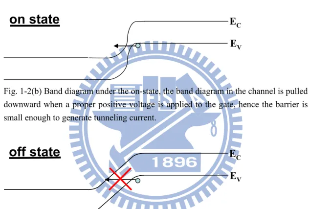
Tunneling FET (T-FET)
mechanism, the T-FET uses the band-to-band tunneling (BTBT) in the source
junction as the current control mechanism. As shown in Fig.1-2a, the T-FET also has
a gated P-I-N structure similar to the I-MOS, but the intrinsic channel is completely
overlapped by the gate. Figures 1-2b&c show the band diagrams of the on and off
states of operation, respectively. In the off state, the reversed biased P-I-N diode
provides a large resistance between source and drain, which results in small leakage
current. In the on state, owing to the sufficiently high gate voltage applied, the
channel potential is pulled downward and a tunneling junction is formed at P-I
junction, thus turning on the T-FET (N-type). However, the insufficient on-state
current represents a major issue for T-FETs. Since the BTBT rate is highly sensitive
to the bandgap (Eg) of the channel material used in the T-FET device, it is difficult
for Si-channel devices to acquire sufficient on-state current with its rather high Eg. In
order to have sufficient on-state current competitive to modern CMOS devices,
narrow bandgap material such as Ge is required.
1.2.3
Suspended Gate MOSFET (SG-MOSFET)
of the gate, while the gate is suspended over the gate oxide. Owing to the low
dielectric constant of the air gap and thus a large EOT, the SG-MOSFET has
extremely low gate leakage in the off state. By increasing the gate voltage, the
positive charges are built in the gate (while the same quantity of negative charges are
generated in the channel surface), resulting in an electrostatic force to pull the gate
downward toward the channel. When the gate voltage is less than the “pull-in
voltage” Vpi, the electrostatic force is balanced by the elastic force. Once the gate
voltage is larger than Vpi, the electrostatic force overcomes the elastic force, the gate
will connect to the gate oxide. When this happens, the gate capacitance increases
abruptly. Hence the threshold voltage is reduced, resulting in the abrupt increase in
drain current. Owing to the abrupt increase of current, the SG-MOSFET has potential
to be used as MEMS switches [18]. Besides, under special operation mode and
measurement technique, the SG-MOSFET has applications such as memories [18] [22]
and sensors [23] [24] [25].
1.3 Motivation
major problem in device scaling [16]. In the above section, some concepts have been
proposed to overcome this barrier. In this thesis, a new type of NW-TFTs originally
proposed by Advanced Device Technology Laboratory (ADTL), NCTU was
fabricated and characterized [26]. With an additional sacrificial layer, the NW
channels were suspended. The operation principle is similar to the SG-MOSFET,
which uses the gate voltage to modulate the equivalent gate capacitance and switch
the operation modes. In this thesis, we will focus on studying the switching behavior
of the suspended NW-channel TFTs.
1.4 Organization of This Thesis
In this thesis, the overview of the NWs and low S.S. devices are described in
Chapter 1. In Chapter 2, we will explain the device structure investigated in this work
and the process flow of device fabrication. In Chapter 3, we discuss the characteristics
of the suspended NW structure. The influences of thickness of the sacrificial layer to
the suspended NW are also discussed. In Chapter 4, we summarize the major findings
Chapter 2
Device Fabrication
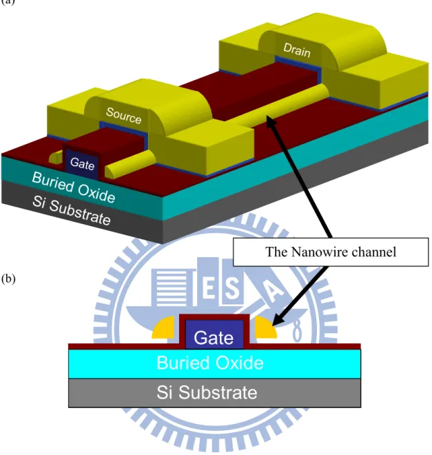
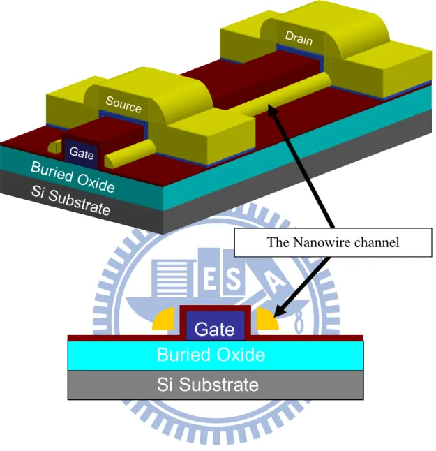
2.1 Device Structure and Process Flow
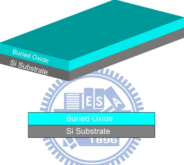
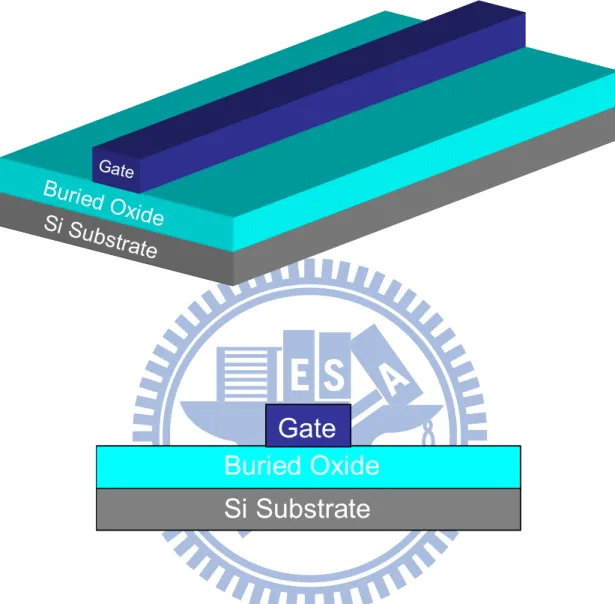
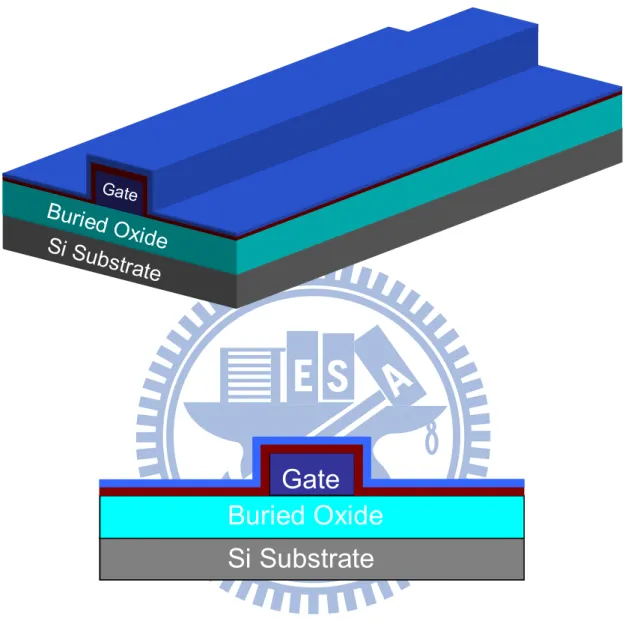
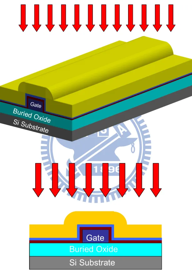
Figure 2-1 shows the stereo and the cross-sectional views of the proposed NW
device. It adopts a side-gate scheme in which two NW channels are formed floating
on the sidewall of the gate. Note the unique feature of the device that the NW
channels are suspended and their position could be modulated by the gate bias. The
gate is capped with an ultra-thin nitride to prevent direct contact of the gate and the
channel. Source and drain (S/D) regions lying across the gate are defined
simultaneously with the NW channels in a self-aligned manner using a novel process
flow described below.
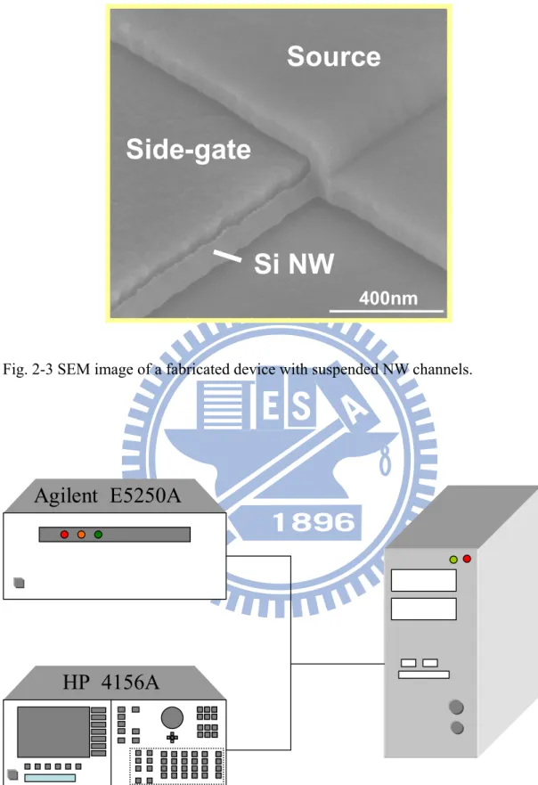
Fabrication of the NW devices characterized in this thesis started on 6-inch
(100)-Si wafers capped with 100nm-thick wet oxide, as shown in Fig. 2-2(a),
followed by the deposition of a 100 nm-thick in-situ n+ doped poly Si film by the low
pressure chemical vapor deposition (LPCVD). Afterwards, reactive plasma etching
RCA clean process, silicon nitride/ TEOS oxide stacked layer was deposited by
LPCVD to serve as gate dielectric layer and sacrificial layer, respectively [Fig. 2-2(c)].
Next, a 100nm-thick undoped amorphous silicon (α-Si) layer was deposited [Fig.
2-2(d)]. In order to transfer the α-Si layer into polycrystalline state, an annealing
step was performed at 600 °C in N2 ambient for 24 hours. Afterwards, source / drain
(S/D) ion implant was carried out by phosphorous ion implantation with energy of 10
keV and dose of 5x1015 cm-2 [Fig. 2-2(e)]. Subsequently, S/D photoresist patterns
were generated by a lithographic step, and then a reactive ion etching step was applied
to form poly-Si spacer along the sidewall of the gate and S/D patterns simultaneously
[Fig. 2-2(f)]. The poly-Si sidewall spacer structures serves as the nanowire channels
of the device. Next, a wet etching step using diluted HF (DHF) or buffered oxide
etch (BOE) solution, was applied to remove the sacrificial TEOS layer between the
NW channels and silicon nitride layer to form the air gap. In this step, the TEOS
layer overlapped by the S/D regions was also etched. Owing to the fact that the area
of the S/D regions is much larger than that between the NW channels and gate, the
TEOS layer between the NW channels and gate can be completely removed while
most of the TEOS under the S/D patterns still remained after the wet etching step if
the wet etch time is properly controlled. Hence, the NW channels were suspended
suspended channels is shown in Fig. 2-3.
2.2 Measurement Setup and Electrical Characterization
Before the investigation of the electrical characteristics, the measurement
setup and definition of several electrical parameters will be described in this section.
Figure 2-4 shows the configuration of the measured settings. Electrical
characteristics are mainly characterized by the automated measurement setup
constructed by an HP 4156A semiconductor parameter analyzer, an AglientTM 5250A
switch, and Interactive Characterization Software (ICS). During all the
measurements, the temperature was controlled at a stable value by
temperature-regulated chuck.
Based on the transfer characteristics measured at Vd=0.1V, the electrical
parameters including threshold voltage (Vth) and subthreshold swing (S.S.), were
extracted according to their definitions:
The threshold voltage (Vth) is extracted by the constant current method. The
Vth is simply defined as Vg corresponding to a specific drain current (Id) of 1nA, i.e.,
@ 1
th g d
The subthreshold swing (S.S.) can be calculated from the subthreshold current in the weak inversion region by
. . (log ) g d V S S I ∂ = ∂ .
2.3 Operation Principle
In the fabricated device, the motion of the suspended NW channel is controlled by the applied gate voltage (Vg). During the electrical measurements, there are two opposite forces to control the motion of the NW channel. One is the elastic force of the suspended channels. The other is the electrical force between the charges presenting at the gate and that at the suspended channels. Such force is controlled by varying Vg.
Initially the channels are suspended and the gate dielectric consists of the air and the nitride layer. An increase in Vg will induce channel charges and the attractive electrical force between the gate and the channel. Once the Vg is sufficiently large enough, the electrical force may overcome the elastic force. Therefore, the NW channel is pulled toward to the gate nitride. This results in a dramatic increase in the gate capacitance. Hence the threshold voltage is reduced, leading to an abrupt increase of drain current. When the Vg is decreased and becomes sufficiently small, the amount of charges at the channel (and the gate) is too small to sustain the attractive force, the channel may restore to its original suspended state by the elastic force.
Chapter 3
Results and Discussion
3.1 Leakage Current and Mechanisms
The major off-state currents of fabricated NW-TFTs are related to several paths. Figure 3-1 illustrates two possible regions dominating the leakage conduction
in our novel NW-TFTs, according to the previous study [28]. One is the drain/channel
junction (path 1) and the other is the gate-to-drain overlap region (path 2).
The conduction mechanism in the drain/channel junction is via trap-assisted
conduction, which is strongly dependent on the magnitude of the drain bias. Figures
3.2(a)-(c) illustrate three cases according to the strength of electric field at the
drain/channel junction.
Under low electric field, electrons are thermally excited from the valence band
into the midgap states. Then the trapped electrons are emitted to the conduction band
(Fig. 3-2(a)). This is called “pure thermal emission” or “thermal generation”.
Under medium electric field, the drain bias pulls the energy band downward at
can tunnel to the conduction band through the reduced barrier width (Fig. 3-2(b)).
This is called “thermionic field emission”.
Under high electric field, the energy band is pulled further downward at the
drain side. The electrons can tunnel from the valence band to the conduction band
with the aid of the trap states. This is called “field emission” or “tunneling”.
The conduction mechanism in the gate-to-drain overlap region is strongly
dependent on the strength of local field which is determined by the gate and drain
biases. This is known as the gate-induced drain leakage (GIDL). Figure 3-3 shows the
mechanism in different local field strength.
When the voltage difference between the drain and gate (|VGD|) is high, the
strong electric field would lead to trap-assisted tunneling (Fig. 3-3(b)) or
band-to-band tunneling (Fig. 3-3(c)).
The major conduction path can be identified by investigating the dependence
of device leakage current with the same channels on the gate-to-drain overlap area.
For the leakage mechanism through path 2, the dependence is linearly proportional to
the gate-to-drain overlap area. For the leakage mechanism through path 1, the
leakage current is independent of the gate-to-drain overlap area.
To identify the leakage path, the normalized leakage currents of the fabricated
width”, as shown in Fig. 3-4. The “gate width” refers to the planar width of the gate
pattern and the main gate-to-drain overlap area is proportional to the “gate width”, as
shown in Fig. 3-4(b). From Fig. 3-4, we can see that the off-state current is
proportional to the gate-to-drain overlap area. This suggests that the major conduction
of off-current is through the gate-to-drain overlap area (path 2).
3.2 Basic Transfer Characteristics
The operation principles of the suspended NW-TFTs are similar to the suspended
gate (SG)-MOSFETs. In this work n+ poly-Si side-gate is used to modulate the
channel potential. Thus the electrical force between the charges present at the gate and
the suspended channels pulls the suspended channels toward the gate dielectric and
turns on the device. Figs. 3-5 & 3-6 show the transfer characteristics of two suspended
NW devices with different air-gap thickness (comparisons of the transistors’ major
parameters are given in Table 3-1) but same nitride thickness of 19.8 nm. In Fig. 3-5,
the device with 4.5 nm air gap thickness shows on/off current ratio of 4.64×10⁵ and
minimum S.S. of 185 mV/dec at the low-current subthreshold regime. In Fig. 3-6, the
ratio and minimum S.S. of 142 mV/dec. In the figures the extracted S.S. values are
unusually small based on the previous experience of the related studies carried out in
our group. To make this clear, Fig. 3-7 shows the transfer characteristics of a device
without stripping the TEOS oxide (i.e., non-suspended channel). The device thus has
gate dielectric consisting of 35nm oxide/11nm nitride. Although, due to the air gap,
the nominal equivalent oxide thickness (EOT) of the device shown in Fig. 3-6 (110.4
nm) are much thicker than the device characterized in Fig. 3-7 (40.7 nm), the S.S. is
not reduced accordingly. Such phenomenon is postulated to be related to the action of
the suspended channels during operations.
However, the switching behaviors of the two devices shown in Figs. 3-5 and 3-6
are not as abrupt as that of the suspended gate (SG) MOSFET (i.e. S.S. almost 0) [18].
As can be seen in the figures, the fabricated devices show lower S.S. at the low
subthreshold current regime. Figure 3-8 shows the S.S. as a function of ID for the
devices characterized in Figs. 3-6 and 3-7. Throughout the ID range we can see the S.S.
of the suspended channel device is always lower than that of the device with
oxide/nitride gate dielectric. For the suspended channel device, the lowest S.S. point
(142 mV/dec) in Fig. 3-7 occurs when the suspended NW channels contact the gate
nitride, and then the S.S. increases with ID when ID is below 1×10⁻¹⁰ A, similar to that
channels are further attracted toward the gate nitride and the portion of the NW
channels in contact with the gate nitride increases gradually. One interesting point
worth noting is that the S.S. seems to “oscillate” when ID is larger than 1×10⁻¹⁰ A for
the suspended channel device, a phenomenon not clearly exhibited for the other
device shown in Fig. 3-8. This is attributed to the oscillation of the NW channels due
to the interaction of elastic force and electrostatic force as VG is sweeping, as shown
in Fig. 3-9. This can be regarded as another indication of the action of the suspended
channel.
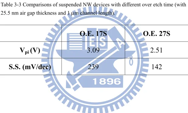
Figs. 3-10 and 3-11 illustrate the transfer characteristics of NW devices with air
gap of 4.5 nm and 22.5 nm, respectively. In the two figures the NW channels of the
devices are formed with two different over-etch time. As mentioned in last chapter,
the over-etch time during the NW-channel formation controls the dimension of the
NW channel. Longer over-etch time implies smaller NW dimensions which may
provide different elastic constant. Both Fig.3-10 and Fig. 3-11 show slightly lower
pull-in voltage and lower S.S. for the devices with longer over-time (see Tables 3-2
and 3-3). Here the pull-in voltage is defined as the gate voltage with the smallest S.S.
in the measurements. Moreover, in Fig. 3-11 significant difference in on-current
between the two devices is also observed: despite the slimmer NW channels, the one
suspected to be caused by the fact that a larger portion of the slimmer NW channels is
connected with the gate nitride as the gate voltage is high due to their higher
flexibility, hence the drive current is larger. Such difference is not obvious in Fig. 3-10
owing to the much smaller air gap. The above discussion implies that the suspended
NW channels are not entirely in contact with the gate nitride even when the device is
turned on. The higher EOT in the channel regions near the drain side and source side
may limit the on-current.
Figure 3-12 shows the transfer characteristics of the suspended-channel devices
with different channel length. As can be seen in the figure, the pull-in voltage
decreases as the channel length increases. This is owing to the presence of the air gap
and therefore the large EOT (110.4 nm) which results in the severe short-channel
effects.
3.3 Hysteresis Phenomenon
3.3.1 Characteristics of Hysteresis
In this section, we discuss the hysteresis phenomenon of the suspended-channel
VG sweeping from -2 V to 7 V as those addressed in previous section. The reverse
sweep measurement refers to the VG sweeping from 7 V to -2 V. It can be seen that the
transfer characteristics of the reverse sweep do not coincide with the trace of forward
sweep, resulting in the hysteresis phenomenon. In the example shown in Fig. 3-13, a
Vth hysteresis window larger than 2 V is obtained.
Fig. 3-14 illustrates the transfer characteristics of a device with different
sweeping range of VG. Again, each set of transfer characteristics consists of the
forward and reverse sweeping curves. As can be seen in the figure, the three forward
sweep curves with a narrower sweeping range are basically overlapping with the one
with the widest sweeping range. For the reverse sweeping, the curves are separate and
dependent on the largest VG of the sweeping range (i.e., the starting point). As can be
seen in the figure, at a fixed VG the drain current is higher for the curve swept from a
higher VG value, implying a larger portion of the NW channels contacting with the
gate nitride. Starting from a higher VG implies a stronger electrostatic force exerted on
the suspended NW channels due to a higher amount of charges induced in the NW
channels. To release those charges (and thus the NW channels), a higher amount of
shift in VG would be needed to release the suspended NW channels.
To test the reproducibility, Fig. 3-15 illustrates the characteristics of three
demonstrated in the figure. It also shows that the suspended channel would not stick
to the gate nitride in the reverse sweeping.
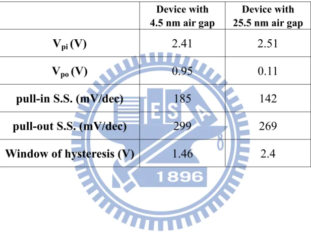
The characteristics of hysteresis window with different air gap thickness (4.5 nm
and 22.5 nm) are compared in Fig. 3-16. The hysteresis window is defined by the VG
difference at Id = 1×10⁻⁹ A, and the extracted data are listed in Table 3-4. The device
with 22.5 nm air gap thickness shows larger hysteresis window owing to the
requirement for a larger VG to pull in the suspended NW channel. The initial current
of the reverse sweep is reduced and not equal to the on-current of the forward sweep.
This is due to internal program setting that does not start the reverse sweep
immediately after the forward sweep. This problem can be eliminated by setting a
consecutive "dual sweep" option by which reverse sweep is executed immediately
after forward sweep (as evidenced in Fig. 3-14).
Fig. 3-17 shows the transfer characteristics of devices with different channel
length under consecutive forward and reverse sweeping measurements. The
differences in transfer characteristics of forward sweeping among the devices are
owing to Vth roll-off due the large EOT of gate dielectric. During the reverse
sweeping, the long channel device (e.g., 1 μm) shows gradual transition in transfer
characteristics, while the two devices with shorter channel exhibit an abrupt pull-out
elastic (restorative) force in the shorter-channel devices, and the NW channels are
pulled away from the gate nitride more easily as VG is swept to a sufficiently low
value. Also can be seen in the figure is that the off-state current of reverse sweep is
higher than that of forward sweep. A postulation about this observation is the flowing
out of the remaining charges stored in the NW channels.
3.3.2 Hysteresis Mechanism
In the previous sections, the hysteresis characteristics of suspended-channel
devices have been discussed. The origin of hysteresis in the poly-Si channel devices
has been proposed recently [30]. The hysteresis phenomenon in poly-Si channel
devices is owing to the electron trapping and de-trapping process in the traps of the
poly-Si channel. However, the Vth difference between the forward and reverse
sweeping is small (~ 0.4 V) [31] and cannot explain our observation in this study. As
mentioned in the previous section, the fabricated devices show a much larger
hysteresis window (at least 1.46 V). This is clearly related to the motion of the
suspended channels during forward and reverse sweeping measurements. Based on
Figure 3-18 shows again the transfer curves illustrated in Fig. 3-13 to help
illustrate the operation of the device described below. Figures 3-19(a)~(c) illustrate
the pull-in mechanism of the suspended-channel device operated under forward
sweeping. In the beginning, the device is in the off-state with a low VG (i.e. VG = 0V).
Hence the suspended NW channels and gate nitride are separated by the air gap (Fig.
3-19(a)). As the VG increases, the electrons are induced in the suspended NW
channels and leads to the attractive electrostatic force between the suspended NW
channels and gate. As such force is sufficiently large it could pull the suspended NW
channels to contact the gate nitride. However, the contact with gate nitride occurs
initially at the central region of the suspended NW channels (Fig. 3-19(b)). This leads
to a sudden increase in drain current, as indicated by the point A in Fig. 3-18. As VG
increases further (region B in Fig. 3-18), the portion of NW channels contacted with
the gate nitride increases gradually (Fig. 3-19(c)), further increasing the drain current.
In the beginning of the reverse sweep (region C in Fig. 3-17), the device is still in
on-state and most of the NW channels remain in contact with the gate nitride. A
lowering in VG tends to repel the charges stored in the channel and thus the attractive
electrostatic force between the NW channels and the gate nitride is reduced. As VG is
swept to a sufficiently low value (region D in Fig. 3-17), the device starts to turn off
be released from the gate nitride and returned to the suspended state. As the channel is
shorter (see, for example, the devices with channel length of 0.4 and 0.7 micron meter
in Fig. 3-17), such pull-out action may occur suddenly and lead to an abrupt decrease
in drain current.
3.4 The Suspended NW Channel TFT with Larger Air Gap
From the results shown in the previous discussions, we can see that the thickness
of the air gap plays an important role in the hysteresis window. In general, the transfer
characteristic of the device with a thicker air gap shows a larger hysteresis window. In
a pervious work [27] the results of simulation on analyzing the characteristics of
SG-MOSETs also confirm this trend (Fig. 3-20). Here, we further discuss the
characteristics of suspended NW channel device with a larger air gap. Figure 3-21(a)
shows the transfer characteristics of a fabricated device with gate dielectric consisting
of 11 nm gate nitride and 35 nm air gap. Owing to the large gap, the pull-in action of
the suspended NW channel does not occur until VG = 13.6 V. Although the transfer
characteristics show abrupt switching, the high VG requirement becomes a
current (about 1×10⁻⁹ A), as shown in the figure. Figure 3-21(b) shows the results of
the second measurement performed on the device. The overlap of the forward and
reverse sweeping curves implies that the suspended NW channels are stuck to the gate
nitride. This would be ascribed to the large surface adhesion force that the elastic
force of the NW channels cannot overcome to return to the suspended state. The high
VG during forward sweep leads to the existence of such high surface adhesion force,
Chapter 4
Conclusion and Future Work
4.1 Conclusion
In this thesis, a new TFT structure featuring suspended NW channels was proposed and successfully demonstrated. The device features a side-gate
configuration and the formation of NW channels is realized by a simple and low cost
sidewall spacer etching technique. The suspension of the NW channels is achieved by
stripping off the sacrificial oxide between the NW channels and the gate nitride layer.
The fabricated devices show hysteresis phenomenon in the transfer characteristics due
to the action of the suspended NW channels. The hysteresis characteristics are
strongly dependent on the NW dimensions, channel length, as well as the thickness of
the air gap. For the device with smaller NW’s cross sectional dimensions, better
performance is obtained. This is attributed to the higher flexibility of the smaller NW
channel so that a larger portion of the slimmer NW channels is connected with the
gate nitride as the gate voltage is high. With a reasonable air gap thickness (25.5 nm),
Also, a better S.S. is presented despite the higher EOT of gate dielectric. Oscillation
phenomenon of S.S. due to the motion of the NW channels is also observed. A model
taking into account the gradual contact procedure of suspended NW channels with
gate nitride owing to the electrostatic force is proposed to explain the experimental
observations.
4.2 Future Work
The development and characterization of a novel suspended-channel device
have been carried out in this thesis. To improve the performance of the device, a new
layout of the devices is proposed. As shown in Fig. 4-1, the new layout of the
suspended NW channels devices have S/D extensions existing at the two sides and an
intrinsic channel at the central part of the NW channels. With the addition of the S/D
extensions, the suspended NW channels would contact the gate nitride more
intimately. This scheme would allow a significant increase in the portion of the
intrinsic channels in contact with the gate nitride during device operation (Fig. 4-1(b)),
further lowering in the threshold voltage and S.S. is expected. Moreover, the parasitic
References
[1] D. J. Frank, R. H. Dennard, E. Nowak, P. M. Solomon, Y. Taur, and H. S. P.
Wong, “Device Scaling Limits of Si MOSFETs and Their Application
Dependencies,” Proc. IEEE , vol.89, pp. 259-281, 2001.
[2] F. L. Yang et al. “5nm-Gate Nanowire FinFET,” VLSI Symp. Tech. Dig. , pp.
196-197, 2004.
[3] X. Duan, Y. Huang, and C. M. Lieber, “Nonvolatile Memory and Programmable
Logic from Molecule-Gated Nanowires,” Nano Lett., vol. 2, pp. 487-490, 2002.
[4] X. Duan, C. Niu, V. Sahi, J. Chen, J. W. Parce, S. Empedocles, and J. L. Goldman,
“High-Performance Thin-Film Transistors Using Semiconductor Nanowires and
Nanoribbons,” Nature, vol. 425, pp. 274-278, 2003.
[5] Y. Cui, Q. Wei, H. Park, and C. M. Lieber, “Nanowire Nanosensors for Highly
Sensitive and Selective Detection of Biological and Chemical Species,” Science,
vol. 293, pp. 1289-1292, 2001.
[6] Z. Li, Y. Chen, X. Li, T. I. Kamins, K. Nauka, and R. S. Williams,
“Sequence-Specific Label-Free DNA Sensors Based on Silicon Nanowires,” Nano
Lett., vol. 4, pp. 245-247, 2004.
[7] M. C. McAlpine, R. S. Friedman, S. Jin, K. H. Lin, W. U. Wang, and C. M. Lieber,
Substrates,” Nano Lett., vol. 3, pp. 1531-1535, 2003.
[8] M. D. Austin, H. Ge, W. Wu, M. Li, Z. Yu, D. Wasserman, S. A. Lyon, and S. Y.
Chou, “Fabrication of 5 Nm Linewidth and 14 nm Pitch Features by Nanoimprint
Lithography,” Appl. Phys. Lett., vol. 84, pp.5299-5301, 2004.
[9] Y. K. Choi, T. J. King, and C. Hu, “A Spacer Patterning Technology for
Nanoscale CMOS,” IEEE Trans. Electron Devices, vol. 49, pp. 436-441, 2002.
[10] M. Law, J. Goldberger, and P. Yang, “Semiconductor Nanowires and Nanotubes,”
Annu. Rev. Mater. Res., vol. 34, pp. 83-122, 2004.
[11]A. M. Morales and C. M. Lieber, “A laser Ablation Method for the Synthesis of
Crystalline Semiconductor Nanowires,” Science, vol. 279, pp. 208-211, 1998.
[12]D. Wang, Q. Wang, A. Javey, R. Tu, H. Dai, H. Kim, P. McIntyre, T.
Krishnamohan, and K. C. Saraswat, “Germanium Nanowire Field-Effect
Transistors with SiO2 and High-κ HfO2 Gate Dielectrics,” Appl. Phys. Lett.,
vol.83, pp. 2432-2434, 2003.
[13]X. Duan, Y. Huang, Y. Cui, J. Wang, and C. M. Lieber, “Indium Phosphide
Nanowires as Building Blocks for Nanoscale Electronic and Optoelectronic
Devices,” Nature, vol. 409, pp.66-69, 2001.
[14]Y. Huang, X. Duan, Q. Wei, and C. M. Lieber, “Directed Assembly of
630-633, 2001.
[15]A. Tao, F. Kim, C. Hess, J. Goldberger, R. He, Y. Sun, Y. Xia, and P. Yang,
“Langmuir-Blodgett Silver Nanowire Monolayers for Molecular Sensing Using
Surface-Enhanced Raman Spectroscopy,” Nano Lett., vol. 3, pp. 1229-1233, 2003.
[16]K. Gopalakrishnan, P. B. Griffin, and J. D. Plummer, “I-MOS: A Novel
Semiconductor Device with a Subthreshold Slope Lower than kT/q,” IEDM Tech.
Dig. , pp. 289–292, 2002.
[17]W. Y. Choi, J. Y. Song, J. D. Lee, Y. J. Park, and B. G. Park, “100-nm
n-/p-channel I-MOS Using a Novel Self-Aligned Structure,” IEEE Electron
Device Lett., vol. 26, no. 4, pp. 261–263, 2005.
[18]N. Abele, N. Fritschi, K. Boucart, F. Casset, P. Ancey, and A. M. Ionescu,
“Suspended-Gate MOSFET: Bringing New MEMS Functionality into Solid-State
MOS Transistor, ” IEDM Tech. Dig., pp. 479–481, 2005.
[19]P. F. Wang, K. Hilsenbeck, T. Nirschl, M. Oswald, C. Stepper, M. Weiss, D.
Schmitt-Landsiedel, and W. Hansch, “Complementary Tunneling Transistor for
Low Power Applications,” Solid State Electron., vol. 48, pp. 2281–2286, 2004.
[20]W. Y. Choi, J. Y. Song, J. D. Lee, Y. J. Park, and B. G. Park, “70-nm
Impact-Ionization Metal–Oxide–Semiconductor (I-MOS) Devices Integrated with
2005.
[21] C. Shen, J. Q. Lin, E. H . Toh, K. F Chang, P. Bai, C. H. Heng, G.. S. Samudra,
and Y. C. Yeo, ”On the Performance Limit of Impact-Ionization Transistors,”
IEDM Tech. Dig., pp.117-120, 2007
[22] N. Abelé, A. Villaret, A. Gangadharaiah, C. Gabioud, P. Ancey, and A.M. Ionescu,
“1T MEMS Memory Based on Suspended Gate MOSFET,” IEDM Tech. Dig.,
2006.
[23] I. Eisele, and M. Zimmer, “Hybrid-gate Suspended Field-Effect Transistors for
Gas-Sensing, “ Device Research Conference Digest, pp.113-116, 2002.
[24] H. Mahfoz-Kotb, A. C. Salaün, T. Mohammed-Brahim, and O. Bonnaud, “Air-Gap
Polycrystalline Silicon Thin-Film Transistors for Fully Integrated Sensors,“ IEEE
Electron Device Letters, vol. 24, pp. 165-167, 2003.
[25] F. Bendriaa, F. Le Bihan, A.C.Salaün, T. Mohammed-Brahim, O. Bonnaud, ”
Suspended-Gate Polysilicon Thin Film Transistor as Generic Structure for Highly
Sensitive Charged Ambience Sensors,” International Conference on Sensing
Technology, pp. 128-132, 2005.
[26] H. C. Lin, M. H. Lee, C. J. Su, T. Y. Huang, C. C. Lee and Y. S. Yang, “A
Simple and Low-Cost Method to Fabricate TFTs with Poly-Si Nanowire
[27] K. Akarvardar, C. Eggimann, D. Tsamados, Y. S. Chauhan,G. C. Wan, A. M.
Ionescu, R. T. Howe, and H. S. Philip Wong, “Analytical Modeling of the
Suspended-Gate FET and Design Insights for Low-Power Logic, ” IEEE Electron
Devices, vol.55, pp. 48-59, 2008
[28] M. H. Lee, “A Study of Leakage Current and Reliability Issues in Poly- Si
Thin-Film Transistors, ” Ph.D. dissertation, Department of Electronics
Engineering and Institute of Electronics, National Chiao Tung University, 2006
[29] S. H. Kim, H. Kam, C. Hu, and T. J. King Liu, “Germanium-Source Tunnel Field
Effect Transistors with Record High ION/IOFF,” Symposium on VLSl Technology
Digest, pp. 178-179, 2009.
[30] H. C. Lin, C. H. Hung, W. C. Chen, Z. M. Lin, H. H. Hsu, and T. Y. Hunag,
“Origin of Hysteresis in Current-Voltage Characteristics of Polycrystalline Silicon
Thin-Film Transistors,” J. Appl. Phys, vol. 105,pp. 054502, 2009
[31] C. H. Kuo, H. C. Lin, G. J. Li, H. H. Hsu, C. J. Su, and T. Y. Huang “A Novel
Thin-film Transistor with Suspended Nanowire Channels and Side-Gated
Configuration,” accepted by Intl. Conf. on Solid State Device and Materials
Table 3-1Comparisons of suspended NW channel devices with different air gap thickness.
Device with
4.5 nm air gap
Device with
25.5 nm air gap
V
pi(V)
2.41 2.51
S.S. (mV/dec)
185 142
Table 3-2 Comparisons of suspended NW devices with different over etch time (with 4.5 nm air gap thickness and 0.4 μm channel length).
O.E. 17S
O.E. 27S
V
pi(V)
2.8 2.58
Table 3-3 Comparisons of suspended NW devices with different over etch time (with 25.5 nm air gap thickness and 1 μm channel length).
O.E. 17S
O.E. 27S
V
pi(V)
3.09 2.51
Table 3-4 Comparisons of suspended NW channel devices with different air gap thickness.
Device with
4.5 nm air gap
Device with
25.5 nm air gap
V
pi(V)
2.41 2.51
V
po(V)
0.95 0.11
pull-in S.S. (mV/dec)
185 142
pull-out S.S. (mV/dec)
299 269
Window of hysteresis (V)
1.46 2.4
Fig.1-1(a) Schematic views of basic device structure of n-channel I-MOS and the band diagrams of the ON \ OFF state. [17]
Fig.1-1(b) a) An electron arrives at the edge of the strong field region at random time τ1. b) The carrier starts impact ionization and avalanche, thereby generating more
carriers. However, the multiplication process with fewer carriers is strongly fluctuating and random, until the number of carrier reaches a reasonable amount (about 50) and overcome the randomness in multiplication process. c) The multiplication process continues until the device is fully turned on. [21]
Fig. 1-1(c) In order to achieve a reliable circuit operation, failure rate less than 1ppm while the device is on is essential (which means only one failure every million operations). For conventional CMOS, the intrinsic delay of 1ppm operation is just a few picosenconds (or less than one). However, with off-state level of 1 μA/μm, I-MOS needs 10 picoseconds for a 1ppm operation. In the trade off between on/off current ratio and dynamic operation delay, I-MOS does not show advantage over conventional CMOS. [21]
Gate
Gate oxide
N
+Drain
P
+Source
Intrinsic channel
Gate
Gate oxide
N
+Drain
P
+Source
Intrinsic channel
Fig.1-2(a) Schematic view of T-FET device structure.
on state
E
CE
VFig. 1-2(b) Band diagram under the on-state, the band diagram in the channel is pulled downward when a proper positive voltage is applied to the gate, hence the barrier is small enough to generate tunneling current.
off state
E
CE
VFig. 1-2(c) Under the off state, the reverse-biased P-I-N diode provides a large barrier between source and drain, result in a small off current.
Fig. 1-3(a) Bird’s view of a SG-MOSFET. The gate is suspended with anchors at both ends. (b) The mobile gate is controlled by two forces; one is the electrostatic force, and the other is elastic force. (c)Before the Vg reaches Vpi, the electrostatic force is balanced by the elastic force. (d)Once the Vg reaches Vpi, the electrostatic force overcomes the elastic force, and the gate is pulled down toward the gate oxide.[27]
(a)
Si Substr
ate
Buried O
xide
Source Drain GateSi Substr
ate
Buried O
xide
Source Drain Gate (b)Si Substrate
Buried Oxide
Buried Oxide
Si Substrate
Buried Oxide
Buried Oxide
Si Substrate
Buried Oxide
Gate
Si Substrate
Buried Oxide
Gate
Si Substrate
Buried Oxide
Buried Oxide
Si Substrate
Buried Oxide
Buried Oxide
Si Substrate
Buried Oxide
Gate
Si Substrate
Buried Oxide
Gate
Fig. 2-1(a) Schematic view of the NW device. (b) Cross-sectional view of the NW channels and the gate.
(a)
Si Substr
Buried O
xide
ate
Si Substr
Buried O
xide
ate
Si Substrate
Buried Oxide
Si Substrate
Buried Oxide
Fig. 2-2(a) Si substrate capped with buried oxide in Bird’s view and cross-sectional view, respectively.
(b)
Si Substr
ate
Buried O
Gatexide
Si Substr
ate
Buried O
Gatexide
Si Substrate
Buried Oxide
Gate
Si Substrate
Buried Oxide
Gate
Fig. 2-2(b) Gate deposition and definition in Bird’s view and cross-sectional view, respectively.
(c)
Si Substr
ate
Buried O
Gatexide
Si Substrate
Buried Oxide
Gate
Si Substrate
Buried Oxide
Gate
Si Substrate
Buried Oxide
Gate
Si Substrate
Buried Oxide
Gate
Fig. 2-2(c) Gate dielectric and sacrificial layer depositions in Bird’s view and cross-sectional view, respectively.
(d)
Si Substr
ate
Buried O
Gatexide
Si Substr
ate
Buried O
Gatexide
Si Substrate
Buried Oxide
Buried Oxide
Si Substrate
Buried Oxide
Gate
Si Substrate
Buried Oxide
Gate
Si Substrate
Buried Oxide
Buried Oxide
Si Substrate
Buried Oxide
Gate
Si Substrate
Buried Oxide
Gate
Si Substrate
Buried Oxide
Gate
Si Substrate
Buried Oxide
Gate
Si Substrate
Buried Oxide
Gate
Si Substrate
Buried Oxide
Gate
(e)
Si Substr
ate
Buried O
Gatexide
Si Substr
ate
Buried O
Gatexide
Si Substrate
Buried Oxide
Buried Oxide
Si Substrate
Buried Oxide
Gate
Si Substrate
Buried Oxide
Gate
Si Substrate
Buried Oxide
Buried Oxide
Si Substrate
Buried Oxide
Gate
Si Substrate
Buried Oxide
Gate
Si Substrate
Buried Oxide
Buried Oxide
Si Substrate
Buried Oxide
Gate
Si Substrate
Buried Oxide
Gate
Si Substrate
Buried Oxide
Gate
Si Substrate
Buried Oxide
Gate
Si Substrate
Buried Oxide
Gate
Si Substrate
Buried Oxide
Gate
(f)
Si Substr
ate
Buried O
xide
Source Drain GateSi Substr
ate
Buried O
xide
Source Drain GateSi Substrate
Buried Oxide
Buried Oxide
Si Substrate
Buried Oxide
Gate
Si Substrate
Buried Oxide
Gate
Si Substrate
Buried Oxide
Buried Oxide
Si Substrate
Buried Oxide
Gate
Si Substrate
Buried Oxide
Gate
Si Substrate
Buried Oxide
Gate
Si Substrate
Buried Oxide
Gate
Fig. 2-2(f) S/D and NW channels defined by a dry etch step.
(g)
Si Substr
ate
Buried O
xide
Source Drain GateSi Substr
ate
Buried O
xide
Source Drain GateSi Substrate
Buried Oxide
Buried Oxide
Si Substrate
Buried Oxide
Buried Oxide
Si Substrate
Buried Oxide
Gate
Si Substrate
Buried Oxide
Gate
Si Substrate
Buried Oxide
Buried Oxide
Si Substrate
Buried Oxide
Buried Oxide
Si Substrate
Buried Oxide
Gate
Si Substrate
Buried Oxide
Gate
Fig. 2-2(g) Using a wet etch step to remove the sacrificial layer to achieve the NW channels suspension.
Source
Side-gate
Si NW
400nm
Source
Side-gate
Si NW
400nm
Fig. 2-3 SEM image of a fabricated device with suspended NW channels.
Agilent E5250A
HP 4156A
Fig. 2-4 The configuration of the measurement setting, which including a HP 4156A semiconductor parameter analyzer and an AglientTM 5250A switch.
Si Substr
ate
Buried O
xide
Source Drain GateSi Substr
ate
Buried O
xide
Source Drain GateGate-to-Drain
Overlap Region
Path 2
Drain/Channel
Junction
Path 1
(a) Et
Channel
Drain
EC EV (b) EtChannel
Drain
EC EV (b) EtChannel
Drain
EC EVFig. 3-2 Leakage mechanisms in drain/channel junction. (a) Thermal emission. (b) Thermionic field emission. (c) Band-to-band tunneling.
(a) Et Gate Gate Dielectric Drain EC Ev (b) Et Gate Gate Dielectric Drain EC Ev (c) Et Gate Gate Dielectric Drain EC Ev
(a) Gate Width (μm) 0.0 0.5 1.0 1.5 2.0 2.5 ID/ID(Gate Width = 0.5 μm) 0.5 1.0 1.5 2.0 2.5
Normalize to Gate Width = 0.5μm VG = -8V VD = 3V (b)
Gate
Drain
Source
Gate width
Main Gate-to-Drain
Overlap Region
Fig. 3-4 (a) Leakage current as a function of gate width. (b) Schematic of the definitions of gate width and main gate-to-drain overlap region.
V
G(V)
-4
-2
0
2
4
6
8
I
D(A)
10
-1410
-1310
-1210
-1110
-1010
-910
-810
-710
-6Gate nitride 19.8nm
Air gap 4.5nm
L=1
μm
V
D=0.1V
V
G(V)
-4
-2
0
2
4
6
8
I
D(A)
10
-1310
-1210
-1110
-1010
-910
-810
-7Gate nitride 19.8nm
Air gap 25.5nm
L=1
μm
V
D=0.1V
V
G(V)
-5 -4 -3 -2 -1
0
1
2
3
4
5
6
7
8
I
D(A
)
10
-1410
-1310
-1210
-1110
-1010
-910
-810
-710
-6S.S. = 988 mV/dec
V
D= 0.1V
L=1
μm
Fig. 3-7 Transfer characteristics of an NW device with gate dielectric consisting of 35nm-oxide /11nm-nitride. The S.S. is around 988 mV/dec.
ID(A) 10-12 10-11 10-10 10-9 10-8 S.S.(V/dec) 0.0 0.5 1.0 1.5 2.0 2.5 3.0
Without air gap With air gap
VD = 0.1V L=1μm
Source
Drain
Gate
Elastic Force
Electrostatic Force
Elastic Force
Electrostatic Force
Fig. 3-9 Schematic illustration of the oscillation of the suspended NW channels resulted form the interaction of elastic force and electrostatic force.
V
G(V)
-3
-2
-1
0
1
2
3
4
5
6
7
8
I
D(A
)
10
-1410
-1310
-1210
-1110
-1010
-910
-810
-710
-6 O.E. 17s O.E. 27sGate nitride 19.8nm
Air gap 4.5nm
L=0.4
μm
V
D=0.1V
Fig. 3-10 Comparisons of transfer characteristics between two devices with different NW dimensions due to different over-etching time.