IEEE ELECTRON DEVICE LETTERS, VOL. 33, NO. 7, JULY 2012 931
Temperature Dependence of Electron Mobility
on Strained nMOSFETs Fabricated
by Strain-Gate Engineering
Tien-Shun Chang, Tsung Yi Lu, and Tien-Sheng Chao
Abstract—An effective electron mobility improvement that
uses strain-proximity-free technique (SPFT) has been demon-strated using strain-gate engineering. The electron mobility of nMOSFETs with SPFT exhibits a 15% increase over that of coun-terpart techniques. The preamorphous layer (PAL) gate structure on the SPFT showed a further performance boost. The electron mobility exhibits a 52% improvement in nMOSFET using a com-bination of SPFT and PAL gate structure. Furthermore, the gain in electron mobility in the SPFT in combination with PAL gate structure decreases at high temperatures. Gate dielectric interface states and ionized gate impurities inducing carrier scattering will play important roles when operating devices under high-temperature conditions.
Index Terms—Mobility, nMOSFETs, strain, temperature.
I. INTRODUCTION
F
OR the development of sub-32-nm CMOS technology [1], mobility improvement by strain engineering will be limited by the narrowing gate space and scaling down of poly-Si gate thickness [2]. Stressor volume limitation and process inte-gration issues are the key challenges for boosting performance in circuit applications. Stress memorization technique (SMT) has been reported to improve electron mobility in nMOSFETs and has been widely studied using different methods [1]–[4]. However, most previous studies have demonstrated the perfor-mance boost without considering the scalability of the gate space in high-density circuits. Longitudinal tensile stress be-comes limited as the stressor volume reaches its saturation point, causing performance degradation [5].Strain-proximity-free technique (SPFT) has been shown to offer performance improvement without the limitation of stres-sor volume in high-density CMOS circuits [6]. In this letter, we demonstrate electron mobility and drain current improvement in nMOSFETs by using SPFT in combination with a preamor-phous layer (PAL) gate structure. Furthermore, we found that the additional thermal annealing process (two-step annealing
Manuscript received October 15, 2011; revised April 4, 2012; accepted April 6, 2012. Date of publication May 2, 2012; date of current version June 22, 2012. This work was supported by the National Science Council, Taiwan, under Contract 100-2221-E-009-012-MY3. The review of this letter was arranged by Editor C. Bulucea.
The authors are with the Department of Electrophysics, National Chiao Tung University, Hsinchu 30010, Taiwan (e-mail: killua0607@yahoo.com.tw; tyliuf@yahoo.com.tw; tschao@mail.nctu.edu.tw).
Color versions of one or more of the figures in this letter are available online at http://ieeexplore.ieee.org.
Digital Object Identifier 10.1109/LED.2012.2194982
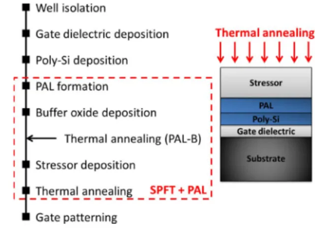
Fig. 1. Process flow for SPFT.
processes) leads to greater stress into the channel. The tempera-ture dependence of electron mobility in the strain-gate structempera-ture is also discussed. In order to extend the applications of devices operating across wide temperature ranges, analysis of the elec-trical properties at various temperatures is required. Phonon scattering dominating electron mobility at high temperatures by lattice vibration is a well-known mechanism in Si. We have found that the gain in electron mobility in SPFT in combination with PAL gate structure decreases at high temperatures. Gate dielectric and Si interface properties are investigated to explain this phenomenon.
II. EXPERIMENT
nMOSFETs were fabricated on 6-in wafers with a resistiv-ity of 15–25 Ω· cm. Grown in a vertical furnace are 2.0 ± 0.1-nm gate oxide and 200-nm poly-Si. The process flow of SPFT, proposed in order to introduce stress into the channel, is shown in Fig. 1. Before patterning of the poly-Si gate, the SPFT was processed by high-tensile stressor deposition, rapid ther-mal annealing using spike annealing at 1050 ◦C, and stressor removal processes. The stressor used in the SPFT was a high-tensile thermal CVD SiN film of 100-nm thickness. The stress level of this film is close to 1.3 GPa. The PAL gate structure is proposed by PAL (PAL-A) in gate using an implantation process. It was inserted into the SPFT process after poly-Si deposition [7]. The dosage split of the As is [40 keV, 5× 1015 cm−2]. The PAL combines a two-step annealing process (PAL-B) with SPFT, which, inserted after the stressor buffer oxide deposition, can bring greater stress into the channel. Dry
932 IEEE ELECTRON DEVICE LETTERS, VOL. 33, NO. 7, JULY 2012
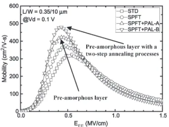
Fig. 2. nMOSFET electron mobility for STD, SPFT, SPFT with PAL-A, and SPFT with PAL-B.
Fig. 3. nMOSFET drain current for STD, SPFT, SPFT with PAL-A, and SPFT with PAL-B under various temperatures. The slope of the fitting curve shows the degradation rate of the drain current.
and wet etching was used in the stressor removal process. After gate patterning, source/drain extension implantation, sidewall spacer, and S/D formation were carried out. A 100-nm thermal CVD tensile SiN CESL was deposited on all transistors. After interlayer-dielectric film deposition and contact patterning, a four-level metallization (Ti–TiN-Al-TiN) was carried out in the PVD system.
III. RESULTS ANDDISCUSSION
The electrical gate oxide inversion thickness is around 29.6± 0.2 Å for all split conditions. The performance im-provement of nMOSFET in SPFT is shown in Fig. 2. Electron mobility is improved by 15% using SPFT, compared to standard devices. Moreover, a significant improvement in mobility in SPFT with PAL-A and SPFT with PAL-B is found, as shown in Fig. 3. It appears that SPFT with PAL-A and SPFT with PAL-B can further improve mobility, by 33% and 52%, respectively.
A simple model is proposed to explain the mechanism of SPFT. It has been reported that the longitudinal tensile stress and vertical compressive stress are the major components of stress in SMT processes [8], [9]. In the SPFT approach, the thermal annealing process transfers high tensile stress from the
Fig. 4. nMOSFET electron mobility for STD, SPFT, SPFT with PAL-A, and SPFT with PAL-B at various temperatures. The slope of the fitting curve shows the degradation rate of electron mobility.
disposable stressor to the gate poly-Si, inducing a plastic strain in the poly-Si. To compensate for this external stress from the disposable stressor, a very high vertical compressive strain is induced in the poly-Si gate. The deformation of the poly-Si is thus expanded in the longitudinal direction and compressed in the vertical direction. This further creates longitudinal tensile stress and vertical compressive stress in the Si channel. After stressor removal, the high longitudinal tensile stress and vertical compressive stress will be memorized in the channel region. This mechanism explains the increased stress resulting from the use of SPFT to improve electron mobility [10]. Moreover, preamorphous poly-Si during the PAL-A and PAL-B processes offers greater compressive strain. Optimization of As implanta-tion energy, dosage, and thermal annealing process at the gate region provides more longitudinal tensile stress and vertical compressive stress to the channel region. This result is similar to the results of previous studies in SPFT with a stacked random-poly-Si-grain gate structure [6].
Fig. 3 shows the measured drain current at various temper-atures. A significant improvement of drain current in SPFT and SPFTs with PAL-A and PAL-B accompanies the improve-ment of electron mobility. It is shown that the drain current is decreased when temperature is increased. This may be at-tributed to phonon scattering and reveals mobility degradation. However, the gains of drain current by SPFTs in combination with PAL-A and PAL-B are also decreased when temperature is increased. The slopes of the fitting curves on STD, SPFT, SPFT with PAL-A, and SPFT with PAL-B are−0.27, −0.32,
−0.63, and −0.96, respectively. The drain current degradation
rate of SPFT with PAL gate structures is more serious than that of STD devices at high temperatures. This means that the strain dependence of mobility improvement becomes weak at high temperatures, particularly on the SPFT in combination with PAL gate structures.
As shown in Fig. 4, electron mobility shows a similar trend with the drain current under various temperatures. The slopes of the STD, SPFT, SPFT with PAL-A, and SPFT with PAL-B are −0.78, −0.82, −1.22, and −1.38, respectively. Higher temperature leads to lower electron mobility gain in the SPFT with the PAL gate structure. The gate dielectric interface state
CHANG et al.: TEMPERATURE DEPENDENCE OF ELECTRON MOBILITY 933
Fig. 5. Charge pumping current for STD, SPFT with PAL-A, and SPFT with PAL-B processes.
density of SPFT with PAL gate structure is checked by measur-ing the charge pumpmeasur-ing current (as shown in Fig. 5). SPFT with PAL-A and SPFT with PAL-B obtained higher interface state density than the STD device. The gate dielectric interface charge and gate impurity play important roles in carrier scat-tering [11], [12]. Electron mobility is dominated by Coulomb scattering at room temperature and low-electric-field region [13]. Moreover, interface charge inducing Coulomb scattering is in proportion to temperature as 1/μint(T )∝ T [14]. Simul-taneously, more ionized impurities in the gate resulting from increasing temperature will enhance remote Coulomb scatter-ing. Therefore, we found that the gain of electron mobility in the SPFT with PAL-A and SPFT with PAL-B is decreased at high temperatures.
IV. CONCLUSION
We have proposed a scheme of two-step annealing pro-cesses for electron mobility improvement that uses the SPFT in combination with a PAL gate structure. The gain of mobility decreases as temperature increases, due to the gate dielectric interface charges and ionized impurities. Therefore, controlling gate impurities and improving interface quality are the keys to continued improvement in future CMOS technology.
ACKNOWLEDGMENT
The authors would like to thank the National Nano De-vice Laboratory, Hsinchu, Taiwan, for the support in deDe-vice fabrications.
REFERENCES
[1] D. V. Singh, K. A. Jenkins, J. Sleight, Z. Ren, M. Ieong, and W. Haensch, “Strained ultrahigh performance fully depleted nMOSFETs with ft of
330 GHz and sub-30-nm gate lengths,” IEEE Electron Device Lett., vol. 27, no. 3, pp. 191–193, Mar. 2006.
[2] S. M. Pandey, J. Liu, Z. S. Hooi, S. Flachowsky, T. Herrmann, W. Tao, F. Benistant, A. See, S. Chu, and G. S. Samudra, “Mechanism of stress memorization technique (SMT) and method to maximize its effect,” IEEE
Electron Device Lett., vol. 32, no. 4, pp. 467–469, Apr. 2011.
[3] T. Y. Lu and T. S. Chao, “Mobility enhancement in local strain channel nMOSFETs by stacked a-Si/poly-Si gate and capping nitride,” IEEE
Elec-tron Device Lett., vol. 26, no. 4, pp. 267–269, Apr. 2005.
[4] A. Wei, M. Wiatr, A. Mowry, A. Gehring, R. Boschke, C. Scott, J. Hoentschel, S. Duenkel, M. Gerhardt, T. Feudel, M. Lenski, F. Wirbeleit, R. Otterbach, R. Callahan, G. Koerner, N. Krumm, D. Greenlaw, M. Raab, and M. Horstmann, “Multiple stress memorization in advanced SOI CMOS technologies,” in Proc. Symp. VLSI Technol., 2007, pp. 216–217.
[5] A. Oishi, O. Fujii, T. Yokoyama, K. Ota, T. Sanuki, H. Inokuma, K. Eda, T. Idaka, H. Miyajima, S. Iwasa, H. Yamasaki, K. Oouchi, K. Yahashi, A. Horiuchi, Y. Takegawa, K. Saki, S. Mori, K. Ohno, I. Mizushima, M. Iwai, S. Yamada, N. Nagashima, and F. Matsuoka, “High performance CMOSFET technology for 45 nm generation and scalability of stress-induced mobility enhancement technique,” in IEDM Tech. Dig., 2005, pp. 229–232.
[6] T. Y. Lu, C. M. Wang, and T. S. Chao, “Enhancement of stress-memorization technique on nMOSFETs by multiple strain-gate engi-neering,” Electrochem. Solid-State Lett., vol. 12, no. 1, pp. H4–H6, Feb. 2009.
[7] T. Y. Lu, T. S. Chang, S.-A. Huang, and T.-S. Chao, “Characterization of enhanced stress memorization technique on nMOSFETs by multiple strain-gate engineering,” IEEE Trans. Electron Devices, vol. 58, no. 4, pp. 1023–1028, Apr. 2011.
[8] P. Morin, C. Ortolland, E. Mastromatteo, C. Chaton, and F. Arnaud, “Mechanisms of stress generation within a polysilicon gate for nMOSFET performance enhancement,” Mater. Sci. Eng. B, vol. 135, no. 3, pp. 215– 219, Dec. 2006.
[9] P. Packan, S. Cea, H. Deshpande, T. Ghani, M. Giles, O. Golonzka, M. Hattendorf, R. Kotlyar, K. Kuhn, A. Murthy, P. Ranade, L. Shifren, C. Weber, and K. Zawadzki, “High performance Hi- K + metal gate strain enhanced transistors on (110) silicon,” in Proc. IEEE IEDM, 2008, pp. 1–4.
[10] T. Miyashita, T. Owada, A. Hatada, Y. Hayami, K. Ookoshi, T. Mori, H. Kurata, and T. Futatsugi, “Physical and electrical analysis of the stress memorization technique (SMT) using poly-gates and its optimization for beyond 45-nm high-performance applications,” in Proc. IEEE IEDM, 2008, pp. 1–4.
[11] P. N. William, P. Su, and K. Goto, “Impact of process-induced strain on Coulomb scattering mobility in short-channel n-MOSFETs,” IEEE Electron Device Lett., vol. 29, no. 7, pp. 768–770, Jul. 2008.
[12] J. Koga, T. Ishihara, and S. Takagi, “Effect of gate impurity concen-tration on inversion-layer mobility in MOSFETs with ultra thin gate oxide layer,” IEEE Electron Device Lett., vol. 24, no. 5, pp. 354–356, May 2003.
[13] S. C. Sun and J. D. Plummer, “Electron mobility in inversion and ac-cumulation layers on thermally oxidized silicon surfaces,” IEEE Trans.
Electron Devices, vol. 27, no. 8, pp. 1497–1508, Aug. 1980.
[14] K. Chain, J. H. Huang, J. Duster, P. K. Ko, and C. Hu, “A MOSFET electron mobility model of wide temperature range (77–400 K) for IC simulation,” Semicond. Sci. Technol., vol. 12, no. 4, pp. 355–358, Apr. 1997.