CMOS IC Realization OF A Low-Cost High-Performance
Frequency Synthesizer
Ching–Chih Kuo
1and Chuei-Liang Tsai
21.Professor of MIS Dept., Hwa Hsia Institute of Technology 2.Manager of R&D Dept.,Syntek Semiconductor Company
ABSTRACT
This paper proposes a frequency synthesizer realized by CMOS integrated circuit and mainly
intended for use in telecommunications including pagers . It features:
1.The whole circuit including analog parts is fully implemented in a single chip by TSMC
0.6μ1P3M CMOS process. This makes cost reduction feasible.
2. Up to 300 MHz input frequency and a wide range of its
programmable divide ratio from 4 to 32767.
3. Up t0 50 MHz reference frequency and a wide range of
its programmable divide ratio from 1 to 1023.
4. Selectable between internal VCO and external VCO.
5. 200 mV
p-pminimum input level required.
The design and simulation of each subcircuit are detailed. The whole system is satisfactorily
verified by testing.
1 INTRODUCTION
For roaming paging service there must be a function of channel scan provided by pagers. To achieve such a function, a frequency synthesizer is needed for scanning a band of frequencies and locking to an appropriate roaming channel [1]. Its application in a pager is shown in Fig.1.
LPF RAM EEPROM CPU DECORDER Driver LCD driver LCD XIN TEST XOUT RCLK VDD3 NCLK Synthesizer LE CON DATA VSS CLK FIN LOCK VDD1 VDD2 DC/DC converter
RF amplifier First mixer
First IF ampliferSecond mixerSecond IF ampliferDiscriminator Wave shaper
Second local oscillator
First local oscillator
1.5V 3V
Power saving pulse1 Power saving pulse2
Fig.1 Typical application of frequency synthesizer in pagers
Commercial frequency synthesizer for pager’s application is available [2]. However, it is not manufactured by using standard CMOS processes and therefore hard to be economically integrated with pager’s decoder and microcontroller to fulfill the increasing need of SOC (System On Chip).
This paper proposes a frequency synthesizer IC realized by TSMC 0.6μ1P3M CMOS process. It is mainly intended for use in telecommunications including pagers. Section 2 introduces its block diagram and the function of each block. Section 3, 4, 5, and 6 present the design and simulation results of input sense amplifier,
prescaler, frequency dividers, and miscellaneous circuits (such as PFD, charge pump, and internal VCO), respectively. Section 7 describes integration concerns of the whole system and gives its simulation and testing results. Finally, Section 8 includes the conclusion of this paper.
2 BLOCK DIAGRAM
The block diagram of frequency synthesizer is depicted in Fig.2. This diagram can be partitioned into three major parts: input sense amplifier, programmable frequency dividers, and miscellaneous circuits. The function of each part is described respectively as follows:
Fig.2 Block diagram of frequency synthesizer for pagers
2.1 Input Sense Amplifier
Owing to the high frequency (up to 300MHz) and small amplitude (as low as 100mV) of the VCO signal sent to FIN pin (see Fig.1 and Fig.2), the conventional inverter with a feedback resistor for amplification has to be extended to multistage one. Thus low power consumption is not attainable. Therefore, we select a structure of direct-drive CMOS ECL receiver [3][4][5] instead to construct our input sense amplifier in order to operate at low power and high frequencies.
2.2 Programmable Frequency Dividers
This part includes a 16-bit shift register to serially receive programmable divide numbers, a 10-bit R-counter
with R-latch to divide the reference frequency fref and a 15-bit N-counter with N-latch to divide the input VCO
frequency fvco. The timing diagram to shift in the divide number DATA is illustrated in Fig.3 where CB
(Control Bit) is used to decide whether the input DATA is 15-bit N number (CB=0) or 10-bit R number (CB=1 and the lower 5 bits are neglected). LE bit is for latch control (Latch Enable). LE=1 makes DATA in the shift register be latched into N-latch or R-latch according to the CB value.
1 2 3 4 5 6 7 8 9 10 11 12 13 14 15 16 MSB LSB CB
CLK DATA LE
Fig.3 Timing diagram of DATA shift
The relationship between fvco and fref when PLL locked is
R
N
f
f
vco
ref (1) 2.3 Miscellaneous CircuitsThis part includes digital phase frequency detector (PFD), charge pump, and internal VCO to construct a phase-locked loop (PLL). When ENVCO=1, the internal VCO is enabled only for self-test. Usually an external VCO (first local oscillator, see Fig.1) is selected (ENVCO=0) in pager applications.
3 DESIGN AND SIMULATION OF INPUT SENSE AMPLIFIER
The input sense amplifier is designed by using CMOS ECL structure [3][4][5] as depicted in Fig.4. The advantages of this structure include:
1. Small power consumption.
2. High voltage gain for amplification at high frequencies (up to 300MHz).
3. High common-mode rejection against variations of power source and P/N MOS threshold voltage Vth.
4. Low circuit complexity.
Fig.4 Circuit diagram of the input sense amplifier using CMOS ECL structure.
After IC layout following TSMC 0.6μ1P3M CMOS rules is completed, HSPICE post-simulation for the input sense amplifier is executed according to the circuit in Fig.5, where the two inverters are placed behind the CMOS ECL receiver for buffering and an external capacitor of 100 pF and an external resistor of 50 Ω are used for input interface.
Fig.5 HSPICE post-simulation circuit of the input sense amplifier
The simulation result for the operating voltage of 3V and the input frequency of 300MHz. is shown in Fig.6. It can be seen that the amplification is sufficient with the input amplitude equal to 100mV.
Fig.6 HSPICE post-simulation result of the input sense amplifier .
4 DESIGN AND SIMULATION OF PRESCALER
Beside the input sense amplifier, there is still a subcircuit operating at the highest frequency in the frequency synthesizer, which is the prescaler used in the 15-bit N counter (see Fig.2). The highest input frequency is specified to 300MHz, so a ÷8 prescaler is used to lower down the operating frequency below 40MHz such that the high frequency processing is concentrated on the prescaler. Here we propose a new approach to design it. Such an approach is different from both the conventional master-slave D flip-flop type and the true single-phase clocking (TSPC)one [6][7][8] and is appropriate for frequencies ranged from 1 KHz to 300 MHz. The approach is characterized by:
1. Two tristate inverters are used to construct dynamic P-latch and N-latch and form a D flip-flop. This structure can avoid the problems of low-frequency limitation and high-frequency glitches encountered in TSPC structure.
2. The glue logic in a stage is separated and pipelined to speed up the overall operation. The above design principles are illustrated in Fig.7.
Fig.7 Design principles of prescaler:
(a) a counter stage
(b) separation of an EX-OR gate
(c) separation of D-FF and pipeline operation of EX-OR
As shown in Fig.7(c), the operation of EX-OR is pipelined into a P-latch and an N-latch that the propagation delay of the cverall stage can be shortened accordingly.
The circuit of ÷8 prescaler is designed as depicted in Fig.8(a)through(d). It features: 1. Constructed by TSMC standard cells.
2. Designed with synchronous type. Dual-modulus method is avoided to extend the lower limit of divide number.
3. Some transistors are added to perform the functions of reset and preset. Reset function is performed in Fig.8(b)&(c) and preset function in Fig.(d).
Fig.8(a) 3 stages of ÷8 prescaler
Fig.8(c) The second stage of ÷8 prescaler
Fig.8(d) The third stage of ÷8 prescaler
Fig.9 HSPICE post-simulation result of the. ÷8 prescaler
After IC layout following TSMC 0.6μ1P3M CMOS rules is completed, HSPICE post-simulation for the prescaler is executed according to the circuit in Fig.8. The simulation result for the operating voltage of 3V and the input frequency of 300MHz is shown in Fig.9. It can be seen from Fig.9 that the ÷8 prescaling function works quite well.
5 DESIGN AND SIMULATION OF FREQUENCY DIVIDERS
There are two frequency dividers in the synthesizer: input frequency divider (15-bit N counter with N latch) and reference frequency divider (10-bit R counter with R latch). Refer to Fig.3, each divider is programmable via input serial data shifted into a 16-bit shift register and stored into its corresponding latch (N latch or R latch).
5.1 15-bit N counter
15-bit N counter is divided into two parts: 3-bit prescaler (discussed previously in Section 4) and the remaining 12-bit counter. The operating frequency in the 12-bit counter is below 40MHz due to ÷8 prescaling for an input frequency up to 300MHz. Hence the conventional look-ahead structure can be employed to implement this counter. Refer to Fig.7(a) for its one-bit stage circuit.
To satisfy the requirement that all the 15 bits be output synchronously for correct operation of the subsequent comparator, careful consideration on timing and buffering has to be made in designing the 12-bit counter. The design of 15-bit comparator is based on “If matched”principle as shown in Fig.10. After reset, counter is incremented on the edge of clock. If the program data and the count number are matched, the counter goes to reset state. Upon reset, counter is set to zero or a fixed number.
If
Matched
Fig.10 Design principle of counter comparator
RESET
Count
UP
Sophisticated efforts are made to design the comparator because the LSB frequency of the 15-bit N counter may be as high as 150 MHz.
After IC layout following TSMC 0.6μ1P3M CMOS rules is completed, HSPICE post-simulation for the
15-bit N counter is executed as shown in Fig.11(a) through (d) where the divide numbers are critically selected to be 10111, 10000, 01010, and 01101 respectively and the input frequency is set to be 300 MHz. The results are satisfactory as shown. as shown.
(a) divide number=10111
(b) divide number=10000
(c) divide number=01010
(d) divide number=01101
Fig.11 HSPICE post-simulation result of the15-bit N counter
5.2 10-bit R counter
10-bit R counter is also divided into two parts: 3-bit prescaler and the remaining 7-bit counter. A 10-bit comparator is needed to reset the 10-bit R counter. The circuit design is similar to that of 15-bit N counter and easier because of its operation at low frequencies (no higher than 50 MHz).
After IC layout following TSMC 0.6μ1P3M CMOS rules is completed, HSPICE post-simulation for the
10-bit R counter is executed as shown in Fig.12(a) and (b) where the divide numbers are critically selected to be 10000 for reference frequency of 50 MHz and 01111 for 2 MHz respectively and the results are satisfactory.
(b) divide number=01111
Fig.12 HSPICE post-simulation result of the10-bit R counter
6 DESIGN AND SIMULATION OF MISCELLANEOUS CIRCUITS
Miscellaneous circuits in our synthesizer include digital phase frequency detector (PFD), charge pump, and internal VCO. Refer to Fig.2 for their positions in the synthesizer.
6.1 Digital phase frequency detector (PFD)
Digital PFD consists of two D flip-flops and several gates as shown in Fig.13. Its outputs N and P drive NMOS and PMOS of the subsequent charge pump respectively.
Fig.13 Circuit diagram of digital PFD
6.2 Charge pump
The charge pump is driven by PFD in order to offer charging and discharging paths for the control pin CON. This CON pin is to be connected to an internal VCO and an external VCO (optional) for providing the VCO control voltage within a PLL. An external lowpass filter must be connected with pin CON for smoothing the control voltage. We use current pump structure to design its circuit as shown in Fig.14. Three NMOS transistors on the right hand provide bias voltage for the current mirror. Six NMOS and PMOS transistors on the left hand construct the current mirror and control switch.
Fig.14 Circuit diagram of charge pump
6.3 Internal VCO
Usually it is very difficult to implement a CMOS VCO in a synthesizer chip. Here we try to make one inside our synthesizer for the purposes of IC self-test and some low-level applications of this chip such as clock generator. As for high-level applications such as telecommunications, external VCO is preferable and recommended.
The circuit diagram of internal VCO is depicted in Fig.15. It is constructed by 5-stage differential amplifiers with the three front stages executing oscillation, the fourth stage performing amplification, and the last stage providing single-ended output. Enabling circuitry is included to enable (ENB=0) or disable (ENB=1) the internal VCO. Refer to Fig.2, when disabling, the signal FIN sent from the external VCO and amplified by the input sense amplifier is selected as the clock source by a multiplexer.
After IC layout following TSMC 0.6μ1P3M CMOS rules is completed, HSPICE post-simulation for the internal VCO is executed. The relationship between control voltage and output frequency is shown in Fig.16 where a monotonously increasing curve is presented as expected.
Fig.16 Relationship between control voltage and output frequency of internal VCO VCO ( X:Control Voltage Y:Frequency )
240 250 260 270 280 290 300 310 1.5 1.6 1.7 1.8 1.9 2 2.1 Volt MHz
7 SYSTEM INTEGRATION, SIMULATION, AND TESTING
7.1 System integrationAfter design and (or) simulation of each block, the whole synthesizer system is integrated as shown in Fig.17. It consists of seven main blocks: DD_ECLRE (input sense amplifier), SH16_NRL (programmable input circuit), F_R_CMP (reference frequency divider), F_N_CMP (input frequency divider), PFD (digital phase frequency detector), CHGPUMP (charge pump), and internal VCO (voltage -controlled oscillator). Some glue logic such as multiplexers and output driving circuits also exists in the integration.
Fig.17 System integration of CMOS synthesizer
7.2 Placement and routing
properly avoid interference from digital part to analog part during placement and routing. Its block placement is specified in Fig.18 where the low-speed digital part is located between the analog part and the high-speed digital part. Also, analog power and ground pins are independent of and placed away from digital ones.
Fig.18 Block Placement for the synthesizer chip
Using 28-lead package type, the I/O pads of this synthesizer IC are arranged as shown in Fig.19. Note that the analog I/O pads are placed on the upper side between pin 18 and pin 25 nearby the analog part.
Mixed-mode IC layout is not an easy task. This task is accomplished according to the following principles:
o VSS (ground). The two layers can absorb most noise passed from
tor with respect to its gate. The decoupling
a high percentage of lateral diffusion during ion ntial pair must be placed as close as possible to eliminate the influence from process
ts on drain and source are placed as many as possible. The above measures can reduce resistive effect.
ynthesizer IC is realized as shown in Fig.20. Its chip size is 2.5 x 2.2 mm2
and its gate count is abou
Fig.20 Layout diagram CMOS synthesizer
1. Any circuit sensitive to interference is circulated by a two-layer guard ring. Such a guard ring is made by
N+connecting to V
DD and P+connecting t
the substrate and keep this region clean.
2. Inside the remaining space of the guarded region, MOS transistors are built in. The source and drain of each MOS are connected together to form a decoupling capaci
capacitor can regulate VDD power and filter out power noise.
3. Metal 2 or Metal 3 can be grounded to form a ground plane and provide shielding effect against EMI/EMC. 4. Minimum MOS length is not used in order to avoid
implementation which may cause nonideal performance. 5. Transistors of differe
parameter gradient.
6. Any MOS transistor of wide width is replaced by several MOS transistors of narrow width in parallel. Also, the metal contac
The whole layout of our CMOS s t 4,000.
of
7.3 System simulation
in Section.3 through Section.6. However, the whole synthesizer system is too large to perform HSPICE post-simulation. Instead, we use Timemill and Powermill of EPIC software to simulate system’s PLL
tion. The simulation conditions are listed below:
r: N=10680 (29B8H)
267 MHz. The Powermill post-simulation result estimates that the total power consumption is about 11 mW.
Fig.21 Timemill post-simulation result of CMOS synthesizer
ert NCLK and RCLK to square waves of 50% duty cycle. So their frequencies are n oscilloscope to observe the two divided clocks. If they are in phase, PLL would be in its locking
ed with CON pin as shown in Fig.22. w:
(A0H) r: see Table 2
VDD power supply: 3V
performance and its power consump
Reference frequency: 4 MHz
Reference divide number: R=160 (A0H)
Input divide numbe
Use internal VCO
VDD power supply: 3V
The Timemill post-simulation result is shown in Fig.21. It can be seen that PLL locking time is about 5 ms. According to Eq.(1), the locked internal VCO frequency must be
7.4 Chip testing
This chip is 28-lead DIP packaged. Its pin assignment is listed in Table 1. Its test environment is set as follows: 1. Use a 8-bit microcontroller to program the divide numbers in IC via DATA, CLK, and LE pins. (see Fig.3) 2. Use a 7474 IC to conv
divided by two. 3. Use a
state.
4. Use a spectrum analyzer to measure VCO frequency. 5. There must be a lowpass filter connect
The testing conditions are listed belo
Reference frequency: 4 MHz
Reference divide number: R=160
Input divide numbe
Table 1 Pin assignment of CMOS synthesizer PIN NO. PIN Name PIN
Type PIN Description 1 VDDA PWR N counter power
2 DN1 OUT N counter LSB (for testing) 3 DN15 OUT N counter MSB (for testing) 4 DR1 OUT R counter LSB (for testing) 5 DVSSA GND Digital ground 6 CLK IN Clock for serial programming 7 LOCK OUT High indicates locking
8 VCO_DOWN OUT High indicates VCO frequency be down 9 VCO_UP OUT High indicates VCO frequency be up 10 VDDB PWR R counter power
11 XOUT OUT Reference clock output 12 XIN IN Reference clock input 13 DVSSB GND Digital ground
14 NCLK OUT N counter divided output clock 15 FVOUT OUT Internal VCO output or external
VCO sense-amplified output (for testing) 16 RCLK OUT R counter divided output clock 17 VDDC PWR Digital circuit power 18 ENVCO IN High selects internal VCO 19 VSS1 GND Analog ground 20 VDD3 PWR Internal VCO power 21 CON OUT VCO control voltage 22 VDD2 PWR Charge pump power 23 VDD1 PWR Sense amplifier power 24 VSS2 GND Analog ground 25 FIN IN Input signal from external VCO 26 LE IN Latch enable for serial programming 27 DATA IN Data for serial programming 28 RSTB IN Low resets chip
Fig.22 Lowpass filter connected with CON pin
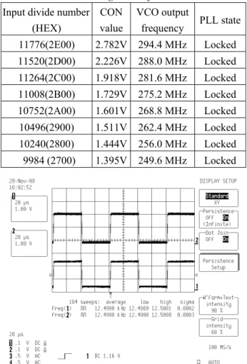
Table 2 lists the testing results of PLL lock and Fig.23 shows the waveforms of divided NCLK and RCLK in locking state. (square wave frequency = 12.5 KHz)
Table 2 Testing result of PLL lock
Input divide number (HEX) CON value VCO output frequency PLL state 11776(2E00) 2.782V 294.4 MHz Locked 11520(2D00) 2.226V 288.0 MHz Locked 11264(2C00) 1.918V 281.6 MHz Locked 11008(2B00) 1.729V 275.2 MHz Locked 10752(2A00) 1.601V 268.8 MHz Locked 10496(2900) 1.511V 262.4 MHz Locked 10240(2800) 1.444V 256.0 MHz Locked 9984 (2700) 1.395V 249.6 MHz Locked
Fig.23 waveforms of divided NCLK and RCLK in locking state.
Fig.24 shows phase jitters appearing on the edges of divided NCLK (upper waveform) and RCLK (lower waveform). It can be seen that the long-term accumulated timing variation due to jitters is no greater than 5 ns. It is believed that jitters can be greatly alleviated if a well-performed external VCO is selected instead of the internal VCO.
Fig.24 phase jitters appearing on the edges of divided NCLK and RCLK
Power consumption of this IC is measured as listed below:
I from VDD1 is not included (Sense AMP)
I from VDD2 and VDD3 = 0.97 mA (VCO+Charge Pump)
I from VDDA = 2.50 mA (N Counter)
I from VDDB = 0.10 mA (R Counter)
I from VDDC is negligible (Other digital circuit)
……… Total = 3.57 mA
Power = V × I = 3 × 3.57 = 10.71 mW
Note that the measured power consumption (10.71 mW) is close to the Powermill-simulated one (about 11 mW). Actually, most of power consumption is due to high-frequency (267 MHz) operation of internal VCO and ÷8 prescaler in N counter. If the operation frequency is reduced to 90 MHz and an external VCO is used instead of the internal VCO, most of power consumption comes from sense amplifier (0.1 mW) and ÷8 prescaler (0.9 mW). Summing up to obtain a value of 1 mW which is comparable to that of NPC5160 synthesizer IC (typically 0.8 mW) [2].
8 CONCLUSION
A CMOS frequency synthesizer IC is successfully designed and implemented by TSMC 0.6μ1P3M CMOS process. Its features include:
1. Up to 300 MHz input frequency and a wide range of its programmable divide ratio from 4 to 32767. 2. Up t0 50 MHz reference frequency and a wide range of its programmable divide ratio from 1 to 1023. 3. Selectable between internal VCO and external VCO.
5. 200 mVp-p minimum input level required.
6. 3V power supply
accumulated timing variation due to jitters, and power consumption. There is still possibility to improve its performance in the following respects:
1. Transistor areas can be further reduced to match the 300 MHz specification because this chip is able to operate at even 400 MHz. Therefore, further reduction in power consumption and chip area is possible. 2. Successful mixed-mode design in this chip makes it possible to build up a well-performed internal VCO
suitable for telecommunication use in the next version.
REFERENCES
[1] European Telecommunications Standards Institute, “ETS 300 133-1, Paging Systems, ERMES, Part 1”, July 1992.
[2] Nippon Precision Circuits, “IC Specification of SM5160 AC/DM Programmable PLL Frequency Synthesizer”, Aug. 1995.
[3] Barbara A. Chappell, “Fast CMOS ECL Receivers With 100-mV Worst-Case Sensitivity”, IEEE JSSC, Vol.23, No.1, pp.59-66, Feb. 1988.
[4] Michel S. J. Steyaert, “ECL-CMOS and CMOS-ECL Interface in 1.2m CMOS for 150-Mhz Digital ECL Data Transmission Systems”, IEEE JSSC, Vol.26, No.1, pp.18-23, Jan. 1991.
[5] Hans-Jurgen Schumacher, “CMOS Subnanosecond True-ECL Output Buffer”, IEEE JSSC, Vol.25, No.1, pp.150-154, Feb. 1990.
[6] Robert Rogenmoser, “An 800-MHz 1-μm CMOS Pipelined 8-b Adder Using TSPC logic-Flip-Flops”, IEEE JSSC, Vol.31, No. 3, Mar. 1996.
[7] Navid Foroudi, “CMOS High-Speed Dual-Modulus Frequency Divider for RF Frequency Synthesis ”, IEEE JSSC, Vol. 30, No.2, Feb. 1995.
[8] Jan Craninckx, “A 1.75-GHz/3-V Dual-Modulus Divide-by-128/129 Prescaler in 0.7-μm CMOS”, IEEE JSSC, Vol. 31, No.7, July 1996.