JEEE ELECTRON DEVICE LETTERS, VOL. 17, NO. 11, NOVEMBER 1996 503
Low-Temperature and Low Thermal
Budget Fabrication
of
Polycrystalline
Silicon Thin-Film Transistors
Hsiao-Yi
Lin,
Member, IEEE, Chun-Yen Chang, Fellow, IEEE,Tan Fu Lei,
Feng-Ming Liu, Wen-Luh Yang, Juing-Yi Cheng, Hua-Chou Tseng,
and
Liang-Po ChenAbstract-A top-gate self-aligned n-channel polycrystalline sil-
icon (poly-Si) thin-film transistor (TFT) has been fabricated with low temperature (5550 C) and low thermal budget process. The ultrahigh vacuum chemical vapor deposition (UHVICVD) grown poly-Si was served as the channel film, the chemical mechanical polishing (CMP) technique was used to polish the channel surface, plasma-enhanced chemical vapor deposited (PECVD) tetraethy- lorthosilicate (TEOS) oxide was used as the gate dielectric, and NH3 plasma was used to passive the device. In this process, the solid phase crystallization (SPC) step is not needed. A field effect mobility of 46 cm2N-s, ON/OFF current ratio of over lo7, and threshold voltage of 0.8 V are obtained. The significant reduction in process temperature and thermal budget make this process advantageous for larger-area-display peripheral driver circuits on glass substrate.
I. INTRODUCTION
OLYCRYSTALLINE silicon (poly-Si) thin-film transis-
P
tors (TFT's) have attracted much attention due to their ap- plications for active matrix liquid crystal displays (AMLCD's) [I]. The key technologies to fabricate TFT's at low temper- ature are the channel preparation, gate dielectric deposition, and doping process. Conventionally, low-pressure chemical vapor deposition (LPCVD) is used for the deposition of the amorphous film followed by solid phase crystallization (SPC) to transform amorphous films to poly-Si. Usually, the SPC process is time consuming ( 1 5 4 8 h), which may seriously affect the throughput and thermal budget of fabrication. On the other hand, the high-quality and low-temperature de- posited gate dielectric are indispensable. Furthermore, how to reduce the post implant anneal time is important for top-gate self-aligned devices. Recently, many methods have been proposed to: a) prepare the channel film (such as laser annealing [2], depositing poly-Si at reduced pressure [ 3 ] ,and catalyzer-assisted growth [4]), b) deposit gate dielectric (such as electron cyclotron resonance (ECR) chemical vapor
Manuscript received January 29, 1996; revised July 8, 1996. This work was supported by the National Science Council, Taiwan, R.O.C., under Contract NSC85-2215-E009-05 1.
H.-Y. Lin, C:Y. Chang, T. F. Lei, J.-Y. Cheng, and H.-C. Tseng are with the Department of Electronics Engineering and Institute of Electronics, National Chiao Tung University, Hsinchu 300, Taiwan, R.O.C.
F.-M. Liu and W.-L. Yang are with the Department of Electrical Engineer- ing, Feng Chia University, Taichung, Taiwan, R.O.C.
L.-P. Chen is with National Nan0 Device Laboratories, Hsinchu 300, Taiwan, R.O.C.
Publisher Item Identifier S 0741-3106(96)08306-I.
deposition (CVD) oxide 151, remote PECVD oxide [6], and plasma tetraethylorthosilicate (TEOS) oxide [7]), and c) realize the doping process (such as in situ doping
[SI,
and plasma ion implantation 191). In the previous work [lo], we fabricated new TFT's using ultrahigh vacuum chemical vapor deposited (UHV/CVD) poly-Si film as the channel material followed by a chemical mechanical polishing (CMP) [ 111. The gate oxide was grown at 850 "C.In this work, a top-gate self-aligned TFT was studied. The UHVKVD deposited poly-Si was used as the channel film and gate electrode, while plasma TEOS oxide was used as
the gate dielectric; no long time post implant annealing was needed. The maximum process temperature is under 550 "C.
11. EXPERIMENTAL
A 500-nm thermally oxidized silicon wafer was used as the initial substrate. A UHV/CVD system was employed to deposit a 80-nm undoped poly-Si film at 550 "C as the channel layer followed by CMP. The UHV/CVD system has
a
base pressure of lops torr anda
deposition pressure of 0.94 mtorr, using SiH4 as the gas source. The CMP system was used to planarize the channel surface. After CMP polishing, the film thickness was reduced to 60 nm, and the rms surface roughness was reduced from 8.0 to 4.2 nm. The grain size is about 80 nm, as determined by plane view transmission electron microscopy (TEM). These films were then defined by a photomask and patterned by a plasma etching for the active area island. A 30-nnn gate oxide was then deposited by PECVD at 300 "C on the channel as the gate dielectric using tetraethylorthosilicate (TEOS) and oxygen as deposition gases. After these steps, a 300-nm undoped poly-Si was deposited by UHV/CVD at 550 "C as the gate material, which was alsodefined by a photomask patterning and by plasma etching. The gate-electrode and source/drain regions were doped by phosphorus implant at an energy of 50 keV and a dose of
5 x 10¹⁵ cmp2. After implantation, a 550 "C anneal was given at N2 ambient for 4 h. The resistivity is around 8 mR-cm of the gate. A NH3 plasma treatment was then given at 300 "@
with the power density of 0.67 W/cm2 for 2 h using PECVD. The 200 nm-thick oxide passivation-layer was also deposited by PECVD system at 300 "C. Finally, contact hole definition and A1 metallization was performed.
504 - - - - - -
.
- - - - I I I IIEEE ELECTRON DEVICE LETTERS, VOL. 17, NO. 11, NOVEMBER 1996
15.2
1.6
are summarized in Table I, where the peak field-effect mobil- ity, /,/,FE, threshold voltage, Vth, subthreshold swing,
ss,
trapdensity, Nt, minimum current, I n l i n , and the on/off current ratio are demonstrated. These values are determined at a drain
G: a Y
70
60 50 404
-20Fig. 1. (a) The I V characteristics of 100-nm TEOS-oxide films deposited by PECVD at 300 " C with the TEOS/Oz flow ratio of' 800:lO. (h) The quasi- and high-frequency C V characteristics. The TEOS oxide was annealed at 400 OC for 30 min at Nz ambient. The capacitance for measurement has a area of 7 x IO-' cm'.
111. RESULTS AND DISCUSSION
Fig. l(a) shows the
IV
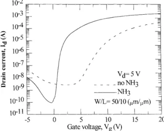
characteristics of the TEOS oxide. The oxide thickness is 100 nm and was annealed at 400 "C for 30 min in nitrogen ambient. The breakdown is defined when the gate current is reaching 1 pA/cm2, and we find that the breakdown field is greater than 8 MV/cm. Fig. l(b) shows the quasi- and high-frequency CV characteristics of the oxide. It is found that the quality of the TEOS oxide is good enough as the gate dielectric. Typical transfer curves of drain currents ( I d ) versus gate voltages (V,) are shown in Fig. 2.This figure illustrates the
IV
characteristics of TFT's with and without NH3 plasma treatment for 2 h. The device has a channel length of 10 pm and a width of 50 pm. After plasma treatment, the performance is dramatically improved. The greatly improved transistor characteristics were not only due to the NH3 passivation, but also due to the improved quality of UHVKVD grown poly-Si films. More device characteristicsdetermined by the I d versus
V,
curve in the linear region atV d = 0.1 V, the trap density.
Nt
is 1.6 x 10¹² cmp2 which was determined byI~[LJ/(V,
-VFB)]
versus l/(Vg -VFB)'
atV d = 0.1 V. The on/off current is 1 . 9 ~ l o 7 and was determined by the gate voltage swing of 20 V and a Vd of 5 V. The low threshold voltage, subthreshold swing, and trap density, in such a small grain (-80 nm) poly-!% TFT, indicate that the UHV/CVD grown poly-Si film is of high quality and can be effectively passivated by NH3 plasma treatment.
IV. CONCLUSIONS
In summary, a new process has been developed for fab- ricating poly-Si TFT's at low temperature and low thermal budget on glass substrate. This process uses UHV/CVD to deposit the channel film, CMP technique to planarize the channel surface, TEOS oxide as the gate dielectric, and NH3 plasma to passive the device. Our results reveal that the usage of these techniques on the device fabrication would be a
powerful approach to realize low-temperature, low thermal budget, and high-throughput process steps. Further study in device process and oxide quality requirements are essential for higher performance devices.
LIN et al.: LOW-TEMPERATURE AND LOW THERMAL BUDGET FABRICATION 505
ACKNOWLEDGMENT
The authors would like to thank the staff of Semiconduc- tor Research Center, National Chiao Tung University, for technique help.
REFERENCES
[ l ] H. Ohshima and S . Morozumi, “Future trends for TFT integrated circuits on glass substrates,” in IEDM Tech. Dig., 1989, vol. 89, p. 157. 121 A. Kohno, T. Sameshima, N. Sano, M. Sekiya, and M. Hara, “High
performance poly-Si TFT’s fabricated using pulsed laser annealing and remote plasma CVD with low temperature processing,” IEEE Trans.
Electron Devices, vol. 42, pp. 251-257, 1995.
[3J H. C. Lin, H. Y. Lin, C. Y. Chang, T. F. Lei, P. J. Wang, R. C. Deng, J. Lin, and C. Y. Chao, “Deposition and device application of in situ boron-doped polycrystalline SiGe films grown at low temperatures,” J.
Appl. Phys., vol. 74, p. 5395, 1993.
[4] H. Matsumura, K. Mimura, and H. Makino, “Low-temperature formation of high-mobility polysilicon TFT by cat-CVD method,” in Znt. Workshop Active-Matrix Liquid-Crystal Display, Proc. AMLCD 95, Japan, 1995,
pp. 89-92.
[SI T. W. Little, K. Takahara, H. Koike, T. Nakazawa, 1. Yudasaka, and H. Ohshima, “Low temperature poly-Si TFT’s using solid phase crystallization of very thin films and an electron cyclotron resonance
chemical vapor deposition gate insulator,” Jpn. J. Appl. Phys., vol. 30,
no. 12B, pp. 3724-3728, 1991.
[6] M. Sekiya, M. Hara, N. Sano, A. Kohno, and T. Sameshima, “High performance poly-crystalline silicon thin-film transistors fabricated using remote plasma chemical vapor deposition of Si02 ,” IEEE Electron
Device Lett., vol. 15, no. 2, pp. 69-71, 1994.
171 Y. Nishi, T. Funai, H. Izawa, T. Fujimoto, H. Morimoto, and M. Ishii, “Characteristics of plasma-enhanced-chemical-vapor-deposition tetraethylorthosilicate oxide and thin-film transistor application,” Jpn.
J. Appl. Phys., vol. 31, no. 12B, p. 4570, 1992.
[8] L. Pichon, F. Raoult, 0. Bonnaud, J. Pinel, and M. Sarret, “Low temperature (5600 “C) polysilicon thin-film transistors having in-situ doped polysilicon source and drain contacts,” IEEE Electron Device
Lett., vol. 16, no. 9, pp. 376-378, 1995.
[9] J. D. Bernstein, S . Qin, C. Chan, and T. J. King, “Hydrogenation of polycrystalline silicon thin-film transistors by plasma ion implantation,”
IEEE Electron Device Lett., vol. 16, no. 10, pp. 421423, 1995.
[lo] C. Y. Chang, H. Y. Lin, T. F. Lei, J. Y. Cheng, L. P. Chen, and B. T. Dai, “Fabrication of thin-film transistors by chemical mechanical polished polycrystalline silicon films,” IEEE Electron Device Lett., vol. 17, no. 3, pp. 100-102, 1996.
[111 M. Cao, S . C. Kuehne, K. C. Saraswat, and S . S . Wong, “A low ther-
mal budget polysilicon thin-film transistor using chemical mechanical polishing,” in SID Con$ Record 1994, Int. Display Research Conf Int. Workshops on Active Matrix LCD’s and Display Materials, Monterey,