N A N O E X P R E S S
Open Access
On the direct insulator-quantum Hall transition in
two-dimensional electron systems in the vicinity
of nanoscaled scatterers
Chi-Te Liang
1*, Li-Hung Lin
2, Kuang Yao Chen
1, Shun-Tsung Lo
1, Yi-Ting Wang
1, Dong-Sheng Lou
3, Gil-Ho Kim
4,
Yuan-Huei Chang
1, Yuichi Ochiai
5, Nobuyuki Aoki
5, Jeng-Chung Chen
3, Yiping Lin
3, Chun-Feng Huang
6,
Sheng-Di Lin
7, David A Ritchie
8Abstract
A direct insulator-quantum Hall (I-QH) transition corresponds to a crossover/transition from the insulating regime to a high Landau level filling factorν > 2 QH state. Such a transition has been attracting a great deal of both
experimental and theoretical interests. In this study, we present three different two-dimensional electron systems (2DESs) which are in the vicinity of nanoscaled scatterers. All these three devices exhibit a direct I-QH transition, and the transport properties under different nanaoscaled scatterers are discussed.
Introduction
The simultaneous presence of disorder and a strong enough magnetic fieldB can lead to a wide variety of interesting physical phenomena. For example, the inte-ger quantum Hall effect is one of the most exciting effects in two-dimensional electron systems (2DES), in which the electrons are usually confined in layers of the nanoscale [1]. In an integer quantum Hall (QH) state, the current is carried by the one-dimensional edge channels because of the localization effects. It has been shown that with sufficient amount of disorder, a 2DES can undergo a B-induced insulator to quantum Hall transition [2-5]. Experimental evidence for such an insu-lator-quantum Hall (I-QH) transition is an approxi-mately temperature (T)-independent point in the measured longitudinal resistivity of a 2DES [3-5]. The I-QH transition continues to attract a great deal of inter-est both experimentally and theoretically as it may shed light on the fate of extended states [6-10], the true ground state of a non-interacting 2DES [2], and a possi-ble metal-insulator transition in 2D [11,12].
It is worth pointing out that in order to observe an I-QH transition separating the zero-field insulator from the QH liquid, one needs to deliberately introduce
strong disorder within a 2DES. The reason for this is that the localization length needs to be shorter than the sample size. In the study by Jiang and co-workers [2], a 2DES without a spacer layer in which strong Coulomb scattering exists was used. Wang et al. utilized a 30-nm-thick heavily doped GaAs layer so as to allow the posi-tively charged Si atoms to introduce long-range random potential in the 2DES [3]. Hughes et al. have shown that when a Si-doped plane was incorporated into a 550-nm-thick GaAs film, a deep potential well can form in which the 2DES is confined close to the ionized donors and is therefore highly disordered [4]. It has been shown that by deliberately introducing nanoscaled InAs quan-tum dots [13] in the vicinity of a modulation-doped GaAs/AlGaAs heterostructure, a strongly disordered 2DES which shows an I-QH transition can be experi-mentally realized [14,15].
The transition/crossover from an insulator to a QH state of the filling factorν > 2 in an ideal spinless 2DES can be denoted as the direct I-QH transition [16-19]. Such a transition has been attracting a great deal of interest and remains an unsettled issue. Experimental [16-19] and theoretical results [9,10] suggest that such a direct transition can occur, and it is a quantum phase transition. However, Huckestein [20] has argued that such a direct transition is not a quantum phase
* Correspondence: [email protected]
1Department of Physics, National Taiwan University, Taipei 106, Taiwan
Full list of author information is available at the end of the article
© 2011 Liang et al; licensee Springer. This is an Open Access article distributed under the terms of the Creative Commons Attribution License (http://creativecommons.org/licenses/by/2.0), which permits unrestricted use, distribution, and reproduction in any medium, provided the original work is properly cited.
transition, but a narrow crossover in B due to weak localization to Landau quantization.
In this study, the authors compare three different elec-tron systems containing nanoscaled scatterers which all show a direct I-QH transition. The first sample is a GaAs 2DES containing self-assembled nanoscaled InAs quantum dots [13,14,21-23].
The second one is a 2DES in a nominally undoped AlGaN/GaN heterostructure [24-33] grown on Si sub-strate [33,34]. Such a GaN-based electron system can be affected by nanoscaled dislocation and impurities [35]. Finally, experimental results on the third sample, a delta-doped GaAs/AlGaAs quantum well with additional modulation doping [36,37], will be presented. All the
experimental results on the three completely different samples show that the direct I-QH transition does not occur with the onset of strong localization due to Landau quantization [20,38]. Therefore, in order to obtain a thorough understanding of the direct I-QH transition, further studies are required.
Experimental details
Figure 1a,b,c show the structures of the three devices, Sample A, Sample B, and Sample C, considered in this study. Sample A is a GaAs/AlGaAs 2DES containing self-assembled InAs quantum dots. Sample B is an AlGaN/GaN heterostructure grown on Si. Such a system is fully compatible with Si CMOS technology and is thus
of great potential applications. Sample C is a delta-doped quantum well with additional delta-doping. Since the electrons in the quantum well in sample B are in close proximity of nanoscaled dislocation and impurities, the 2DES is strongly influenced by these nanoscaled scatterers. In fact, these scatterers provide scattering which is required for observing the I-QH transition [16]. On the other hand, the scatterings in samples A and C are mainly due to the self-assembled quantum dots and the delta-doping in the quantum well, respectively. Recent studies focussing on alloy disorder in AlxGa 1-xAs/GaAs heterostructure [39-41] have shown that
2DESs influenced by short-range disorder provides an excellent opportunity to connect the Anderson localiza-tion theory with real experimental systems [41]. More-over, the nature of disorder may affect scaling behavior in the plateau-plateau (P-P) transition at highB [39-41], and the P-P and I-QH transitions may be considered as the same universality class [42]. Therefore, it may be interesting to investigate the direct I-QH transitions under different scattering types at low magnetic fields. In this article, such low-field direct transitions in sam-ples A, B, and C are compared.
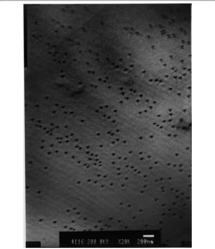
Figure 2 shows a TEM image of the wafer for fabricat-ing Sample A. Very uniform nanoscaled InAs quantum dots can be seen. These nano-scattering centers provide strong scattering in the vicinity of the 2DES in the GaAs. The dimensions of the quantum dot are esti-mated to be 20 nm in diameter and 4 nm in height. Experiments were performed in a top-loading He3 cryo-stat equipped with a superconductor magnet. Four-terminal resistance measurements were performed using standard phase-sensitive lock-in techniques.
Results and discussions
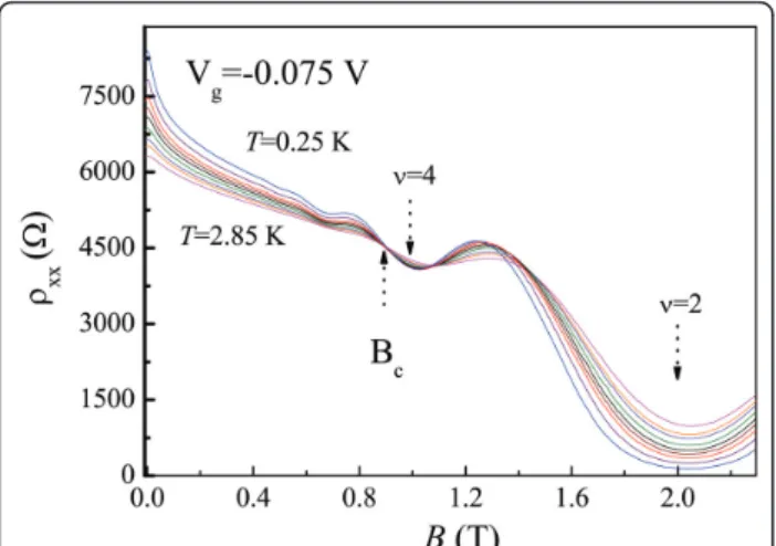
Figure 3 shows the longitudinal magnetoresistivity mea-surements on Sample A as a function of B at various temperatures. It can be seen that at a crossing fieldBc = 0.9 T,rxxis approximatelyT-independent. For B <Bc,
rxxdecreases with increasing temperature, characteristics
of an insulating regime [16]. For B >Bc, rxxincreases
with increasing temperature, and therefore the 2DES is in the quantum Hall regime. As the 2DES enters theν = 4 QH state from the insulating regime, a direct 0-4 tran-sition where the symbol 0 corresponds to the insulator has been observed. It is worth pointing out that before the 2DES enters the ν = 4 QH state, resistance oscilla-tions due to Landau quantization in the insulating regime have already been observed [15,19,21]. Therefore, the experimental results of this study clearly demon-strate that the crossover from localization from Landau quantization actually covers a wide range of magnetic
field, in sharp contrast to Huckestein’s argument [19-21].
As mentioned earlier, a GaN-based electron system can be affected by nanoscaled dislocation and impurities. It is therefore interesting to study such a system. Figure 4 shows magnetoresistance measurements on Sample B as a function of magnetic field at different temperatures. The data deviate slightly from the expected symmetric behavior, i.e.,R(B) = R(-B). The reason for this could be due to slight misalignment of the voltage probes. Never-theless, it can be seen that atBc= 11 Tand -Bc= -11 T,
the measured resistances are approximately temperature independent. The corresponding Landau level filling fac-tor is about 50 in this case. Therefore, a direct 0-50 tran-sition has been observed. Note that even at the highest attainable field of approximately 15T, there is no sign of resistance oscillations due to the moderate mobility of our GaN system. Therefore, the experimental results of this study clearly demonstrate that the observed direct I-QH transition is irrelevant to Landau quantization. Therefore, the onset of Landau quantization does not necessarily accompany the direct I-QH transition, incon-sistent with Huckestein’s model [20].
Figure 5 shows magnetoresistance measurements on Sample C as a function of magnetic field at various tem-peratures. It can be seen that the 2DES undergoes a 0-8 transition characterized by an approximately tempera-ture-independent point in r xxat the crossing fieldBc.
Near the crossing field,rxxis very close torxythoughr
xy-shows a weak T dependence. For B <Bc, no resistance
oscillation is observed. At first glance, our experimental results are consistent with Huckestein’s model. How-ever, it is noted that Landau quantization should be linked with quantum mobility, not classical Drude mobi-lity [36]. Moreover, the observed oscillations forB >Bc
do not always correspond to formation of quantum Hall states. As mentioned in our previous study [36], the observed oscillations can be well approximated by con-ventional Shubnikov-de Haas (SdH) formalism. It is noted that the SdH formula is derived without consider-ing quantum localization effects which give rise to for-mation of quantum Hall state. Therefore, quantum localization effects are not significant in the system under this study. Actually, as shown in Figure 6, the crossing point insxy at around 7.9 Tmay correspond to
the extended states due to the onset of the strong locali-zation effects. Therefore, in this study, the onset of strong localization actually occurs at a magnetic field approximately 4 Thigher than the crossing point.
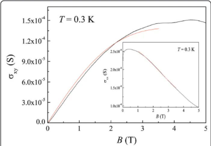
It has been suggested that by converting the measured resistivities into longitudinal and Hall conductivities, it is possible to shed more light on the observed I-QH
transition [5]. Figure 6 shows such results at various tem-peratures. Interestingly, forB < 5 T, sxyis nominallyT
independent. Such data are consistent with electron-elec-tron interaction effects. Over the whole measurement range,sxxdecreases with increasingT, consistent with
electron-electron interaction effects. Unlikesxy,sxxshows a significant Tdependence.
By inspecting the conductivies, previously the authors have studied the renormalized mobility [43] of a GaN-based 2DES at high temperatures (Sample B) [44]. It is
therefore interesting to study such a mobility for both Sample A and Sample C. It has been suggested the elec-tron-electron interaction effects can renormalize the mobilityμ’ given by xy ne B B = + ’ ( ’ ) , 2 2 1 (1) xx eed ne B B = + + ’ ( ’ ) . 1 2 Δ (2)
Figure 7 and the inset to Figure 7 show sxyandsxx ,
together with fits to Equations 1 and 2 over limited ranges for Sample C, respectively. From the fits, it is pos-sible to determine the respective renormalized mobilites as a function of temperature as shown in Figure 8a for Sample C and in Figure 8b for Sample A. The
renormalized mobility calculated using Equation 1 is only slightly larger than that using Equation 2. It may be pos-sible that different mobilities should be taken into account to understand the direct I-QH transition [37,43,45].
Conclusions
In conclusion, the authors have presented studies on three completely different electron systems. In these three samples, the nanoscaled scatterers, in close proximity of the 2DES, provide necessary disorder for observing the direct I-QH transition. In these studies, it has been shown that the crossover from localization to Landau quantization actually covers a wide range of magnetic field. Moreover, the observed direct I-QH transition is not necessarily linked with Landau quanti-zation as no resistance oscillations are observed even up to a magnetic field 4 T higher than the crossing
Figure 3rxx(B) at various temperatures ranging from 0.25 to
2.85 K (Sample A).
Figure 4rxx(B) at various temperatures ranging from 0.28 to
20 K (Sample B).
Figure 5rxx(B) at various temperatures ranging from 0.3 to 4
K (Sample C).rxx at T = 0.3 K and T = 4 K are shown.
Figure 6 Convertedsxx(B) and sxy(B) at various temperatures
field. Most importantly, the onset of strong localization which gives rise to the formation of quantum Hall state does not correspond to the direct I-QH transi-tion. All these three pieces of experimental evidence show that a 2DES in the vicinity of nanoscaled scat-terers is an ideal playground for studying the direct I-QH transition. Furthermore, in order to obtain a thorough understanding of the underlying physics of the direct I-QH transition, modifications of Huckes-tein’s model [20] must be made.
Abbreviations
I-QH: insulator-quantum Hall; SdH: Shubnikov-de Haas; 2DESs: two-dimensional electron systems.
Acknowledgements
This research was supported by the WCU (World Class University) program through the National Research Foundation of Korea (NRF) funded by the Ministry of Education, Science and Technology (Grant No. R32-2008-000-10204-0). C.T.L. acknowledges financial support from the NSC (Grant no: NSC 99-2119-M-002-018-MY3). The authors would like to thank Yi-Chun Su and Jau-Yang Wu for providing help in the experiments.
Author details
1Department of Physics, National Taiwan University, Taipei 106, Taiwan 2
Department of Applied Physics, National Chiayi University, Chiayi 600, Taiwan3Department of Physics, National Tsinghwa University, Hsinchu 300,
Taiwan4Department of Electronic and Electrical Engineering and SAINT,
Sungkyunkwan University, Suwon 440-746, Korea5Graduate School of
Advanced Integration Science, Chiba University, Chiba 263-8522, Japan
6
National Measurement Laboratory, Centre for Measurement Standards, Industrial Technology Research Institute, Hsinchu 300, Taiwan7Department
of Electronics Engineering, National Chiao Tung University, Hsinchu 300, Taiwan8Cavendish Laboratory, J.J. Thomson Avenue, Cambridge CB3 0HE,
UK
Authors’ contributions
CTL, GHK and YHC coordinated the measurements on Sample A. CTL coordinated the measurements on Sample B. KYC performed the measurements on Sample B. JCC and YL coordinated the measurements on Sample C undertaken in Taiwan. YO and NA coordinated early
measurements on Sample C in Japan. CTL, STL and CFH drafted the manuscript. LHL, YTW and DLS performed measurements on Sample C. SDL and DAR grew the MBE wafers. All authors read and approved the final manuscript.
Competing interests
The authors declare that they have no competing interests. Received: 14 August 2010 Accepted: 11 February 2011 Published: 11 February 2011
References
1. von Klitzing K, Dorda G, Pepper M: New Method for High-Accuracy Determination of the Fine-Structure Constant Based on Quantized Hall Resistance. Phys Rev Lett 1980, 45:494.
2. Kivelson S, Lee DH, Zhang SC: Global phase diagram in the quantum Hall effect. Phys Rev B 1992, 46:2223.
3. Jiang HW, Johnson CE, Wang KL, Hannah ST: Observation of magnetic-field-induced delocalization: Transition from Anderson insulator to quantum Hall conductor. Phys Rev Lett 1993, 71:1439.
4. Wang T, Clark KP, Spencer GF, Mack AM, Kirk WP: Magnetic-field-induced metal-insulator transition in two dimensions. Phys Rev Lett 1994, 72:709. 5. Hughes RJF, Nicholls JT, Frost JEF, Linfield EH, Pepper M, Ford CJB,
Ritchie DA, Jones GAC, Kogan E, Kaveh M: Magnetic-field-induced insulator-quantum Hall-insulator transition in a disordered two-dimensional electron gas. J Phys Condens Matter 1994, 6:4763. 6. Laughlin RB: Levitation of Extended-State Bands in a Strong Magnetic
Field. Phys Rev Lett 1984, 52:2304.
7. Khmelnitskii D: Quantum hall effect and additional oscillations of conductivity in weak magnetic fields. Phys Lett 1984, 106A:182. 8. Liu DZ, Xie XC, Niu Q: Weak Field Phase Diagram for an Integer Quantum
Hall Liquid. Phys Rev Lett 1996, 76:975.
9. Sheng DN, Weng ZY: Disappearance of Integer Quantum Hall Effect. Phys Rev Lett 1997, 78:318.
10. Sheng DN, Weng ZY: Phase diagram of the integer quantum Hall effect. Phys Rev B 2000, 62:15363.
11. Kravchenko SV, Kravchenko GV, Furneaux JE, Pudalov VM, D’Iorio M: Possible metal-insulator transition atB = 0 in two dimensions. Phys Rev B 1994, 50:8039.
12. Dobrosavljevic V, Abrahams E, Miranda E, Chakravarty S: Scaling Theory of Two-Dimensional Metal-Insulator Transitions. Phys Rev Lett 1997, 79:455. 13. Chang WH, Lin CH, Fu YJ, Lin TC, Lin H, Cheng SJ, Lin SD, Lee CP: Impacts
of Coulomb Interactions on the magnetic response of excitonic complexes in single semiconductor nanostructures. Nanoscale Res Lett 2010, 5:680.
Figure 7sxy(B) and the fit to Equation 1 for 0 <B < 3.5 T. The
inset showssxx(B) and the fit to Equation (2) for 1 T <B < 3.5 T.
Figure 8 Calculated renormalized mobilities due to electron-electron interaction effects using Equations (1) and (2) for (a) Sample C and (b) Sample A, respectively.
14. Kim GH, Nicholls JT, Khondaker SI, Farrer I, Ritchie DA: Tuning the insulator-quantum Hall liquid transitions in a two-dimensional electron gas using self-assembled InAs. Phys Rev B 2000, 61:10910.
15. Kim GH, Liang CT, Huang CF, Nicholls JT, Ritchie DA, Kim PS, Oh CH, Juang JR, Chang YH: From localization to Landau quantization in a two-dimensional GaAs electron system containing self-assembled InAs quantum dots. Phys Rev B 2004, 69:073311.
16. Song SH, Shahar D, Tsui DC, Xie YH, Monroe D: New Universality at the Magnetic Field Driven Insulator to Integer Quantum Hall Effect Transitions. Phys Rev Lett 1997, 78:2200.
17. Lee CH, Chang YH, Suen YW, Lin HH: Magnetic-field-induced
delocalization in center-doped GaAs/AlxGa1-xAs multiple quantum wells.
Phys Rev B 1998, 58:10629.
18. Huang CF, Chang YH, Lee CH, Chuo HT, Yeh HD, Liang CT, Lin HH, Cheng HH, Hwang GJ: Insulator-quantum Hall conductor transitions at low magnetic field. Phys Rev B 2002, 65:045303.
19. Huang TY, Juang JR, Huang CF, Kim GH, Huang CP, Liang CT, Chang YH, Chen YF, Lee Y, Ritchie DA: On the low-field insulator-quantum Hall conductor transition. Physica E 2004, 22:240.
20. Huckestein B: Quantum Hall Effect at Low Magnetic Fields. Phys Rev Lett 2000, 84:3141.
21. Huang TY, Liang CT, Kim GH, Huang CF, Huang CP, Lin JY, Goan HS, Ritchie DA: From insulator to quantum Hall liquid at low magnetic fields. Phys Rev B 2008, 78:113305.
22. Huang TY, Huang CF, Kim GH, Huang CP, Liang CT, Ritchie DA: An Experimental Study on the Hall Insulators. Chin J Phys 2009, 47:401. 23. Huang TY, Liang CT, Kim GH, Huang CF, Huang CP, Ritchie DA: Probing
two-dimensional metallic-like and localization effects at low magnetic fields. Physica E 2010, 42:1142.
24. Nakamura S, Senoh M, Iwasa N, Hagahama S, Yamada Y, Mukai Y: Superbright Green InGaN Single-Quantum-Well-Structure Light-Emitting Diodes. Jpn J Appl Phys 2 1995, 34:L1332.
25. Wu Y, Keller B, Keller S, Kapolnek D, Kozodoy P, DenBaars S, Mishra U: Very high breakdown voltage and large transconductance realized on GaN heterojunction field effect transistors. Appl Phys Lett 1996, 69:1438. 26. Bulman GE, Doverspike K, Sheppard ST, Weeks TW, Kong HS, Dieringer HM,
Edmond JA, Brown JD, Swindell JT, Schetzina JF: Pulsed operation lasing in a cleaved-facet InGaN/GaN MQW SCH laser grown on 6H-SiC. Electron Lett 1997, 33:1556.
27. Mack MP, Abare A, Aizcorbe M, Kozodoy P, Keller S, Mishra UK, Coldren L, Denbaars S: Characteristics of indium-gallium-nitride multiple-quantum-well blue laser diodes grown by MOCVD. MRS Internet J Nitride Semicond Res 1997, 2:41.
28. Hang DR, Liang CT, Juang JR, Huang TY, Hung WK, Chen YF, Kim GH, Lee JH, Lee JH: Electrically detected and microwave-modulated Shubnikov-de Haas ocsillcations in an Al0.4Ga0.6N/GaN heterostructure.
J Appl Phys 2003, 93:2055.
29. Juang JR, Huang TY, Chen TM, Lin MG, Lee Y, Liang CT, Hang DR, Chen YF, Chyi JI: Transport in a gated Al0.18Ga0.82N/GaN electron system. J Appl
Phys 2003, 94:3181.
30. Cho KS, Huang TY, Huang CP, Chiu YH, Liang CT, Chen YF, Lo I: Exchange-enhanced g-factors in an Al0.25Ga0.75N/GaN two-dimensional electron
system. J Appl Phys 96:7370.
31. Chen JH, Lin JY, Tsai JK, Park H, Kim GH, Youn D, Cho HI, Lee EJ, Lee JH, Liang CT, Chen YF: Experimental evidence for Drude-Boltzmann-like transport in a two-dimensional electron gas in an AlGaN/GaN heterostructure. J Korean Phys Soc 2006, 48:1539.
32. Lin JY, Chen JH, Kim GH, Park H, Youn DH, Jeon CM, Baik JM, Lee JL, Liang CT, Chen YF: Magnetotransport measurements on an AlGaN/GaN two-dimensional electron system. J Korean Phys Soc 2006, 49:1130. 33. Hang DR, Chou MMC, Hsieh MH, Heuken M: Influence of an Advanced
Buffer Layer on the Optical Properties of an InGaN/GaN MQW Grown on a (111) Silicon Substrate. J Korean Phys Soc 2007, 50:797.
34. Chen KY, Liang CT, Chen NC, Chang PH, Chang CA: Weak Localization and electron-electron interaction effects in Al0.15Ga0.85N/GaN High Electron Mobility Transistor Structure. Chin J Phys 2007, 45:616.
35. Schremer AT, Smart JA, Wang Y, Ambacher O, MacDonald NC, Shealy JR: High electron mobility AlGaN/GaN heterostructure on (111) Si. Appl Phys Lett 2000, 76:736.
36. Chen KY, Chang YH, Liang CT, Aoki N, Ochiai Y, Huang CF, Lin LH, Cheng KA, Cheng HH, Lin HH, Wu JY, Lin SD: Probing Landau quantization
with the presence of insulator-quantum Hall transition in a GaAs two-dimensional electron system. J Phys Condens Matter 2008, 20:295223. 37. Chen KY, Liang CT, Aoki N, Ochiai Y, Cheng KA, Lin LH, Huang CF, Li Y-R,
Tseng YS, Yang CK, Lin PT, Wu JY, Lin SD: Probing insulator-quantum Hall transitions by current heating. J Korean Phys Soc 2009, 55:64.
38. Kannan ES, Kim G-Ho, Lin JY, Chen JH, Chen KY, Zhang ZY, Liang CT, Lin LH, Youn DH, Kang KY, Chen NC: Experimental Evidence for Weak Insulator-Quantum Hall Transitions in GaN/AlGaN Two-Dimensional Electron Systems. J Korean Phys Soc 2007, 50:1643.
39. Li W, Csathy GA, Tsui DC, Pfeiffer LN, West KW: Direct observation of alloy scattering of two-dimensional electrons in AlxGa1-xAs. Appl Phys Lett 2003,
83:2832.
40. Li W, Csáthy GA, Tsui DC, Pfeiffer LN, West KW: Scaling and Universality of Integer Quantum Hall Plateau-to-Plateau Transitions. Phys Rev Lett 2005, 94:206807.
41. Li W, Vicente CL, Xia JS, Pan W, Tsui DC, Pfeiffer LN, West KW: Scaling in Plateau-to-Plateau Transition: A Direct Connection of Quantum Hall Systems with the Anderson Localization Model. Phys Rev Lett 2009, 102:216801.
42. Shahar D, Tsui DC, Shayegan M, Shimshoni E, Sondhi SL: A Different View of the Quantum Hall Plateau-to-Plateau Transitions. Phys Rev Lett 1997, 79:479.
43. Minkov GM, Germanenko AV, Rut OE, Sherstobitov AA, Larionova VA, Bakarov AK, Zvonkov BN: Diffusion and ballistic contributions of the interaction correction to the conductivity of a two-dimensional electron gas. Phys Rev B 2006, 74:045314.
44. Liang CT, Lin LH, Huang JZ, Zhang ZY, Sun ZH, Chen KY, Chen NC, Chang PH, Chang CA: Electron-electron interactions in Al0.15Ga0.85N/GaN
high electron mobility transistor structures grown on Si substrates. Appl Phys Lett 2007, 90:022107.
45. Murzin SS: On the phase boundaries of the integer quantum Hall effect. Part II. JETP Lett 2010, 91:155.
doi:10.1186/1556-276X-6-131
Cite this article as: Liang et al.: On the direct insulator-quantum Hall transition in two-dimensional electron systems in the vicinity of nanoscaled scatterers. Nanoscale Research Letters 2011 6:131.
Submit your manuscript to a
journal and benefi t from:
7 Convenient online submission 7 Rigorous peer review7 Immediate publication on acceptance 7 Open access: articles freely available online 7 High visibility within the fi eld
7 Retaining the copyright to your article