14-1
Low Jitter
Butterworth Delay-Locked Loops
Hsiang-Hui Chang, Chih-Hao Sun, and Shen-Iuan Liu
Department of Electrical Engineering & Graduate Institute of Electronics Engineering National Taiwan University, Taipei, Taiwan 10617, R. 0. C.
Abstract
The low jitter Butterworth delay-locked loops (DLLs) are presented in this paper. The proposed Butterworth DLLs can suppress both the jitters generated by the input noise and the voltage-controlled delay line (VCDL) noise without stability considerations. Theoretically, the proposed Buttmorth 2"d-order DLL and 31d-order one could reduce the rms jitter due to the VCDL by a factor of
f i and
2, respectively. In addition, a technique called dynamic bandwidth-adjusting scheme (DBAS) is adopted to shorten the lock time without compromising the jitter performance. The conventional DLL and the proposed ones are simultaneously fabricated at the same die ina
CMOS 0.35-um one-poly four-metal process. Compared with the conventional DLL, the measured rms jitters of the proposed DLLs can be improved by a factor of 1.40 and 1.95,respectively, with an input frequency of 125MHz. The maximum pow& consumption of the proposed DLLs is 32mW.
I. Introduction
Modern CMOS techniques can not only integrate many digital circuits into a system, but also raise the operating clock frequency of the digital systems. However, the higher operating clock will decrease the timing margin for high-performance digital systems. As the timing margin is tight, the timing skews and jitters would make it difficult to synchronize among IC modules. For a conventional DLL, its loop behavior can be usually characterized by a l"-order lowpass transfer function. The input jitter can be attenuated by 20dEYdecade outside the loop bandwidth. Thus, one can narrow the loop bandwidth of a conventional DLL to decrease the influence of the input jitter [I]. However, to narrow the loop bandwidth car, not reduce the jitter caused by the VCDL in the conventional DLL [I]. The proposed Butterworth DLLs could suppress the jitters due to both input noise and the VCDL noise without stability considerations.
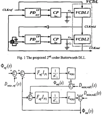
11. The proposed Butterworth DLLs Fig. 1 shows the architecture of the proposed 2"-0rder Buttmorth DLL. A VCDL, which is the same one in the conventional DLL, is divided into two equal parts, i.e., VCDLI and VCDL2 in Fig. 1. The first loop of Fig. 1 is similar to that in conventional DLL, but the generated voltage controlled half the VCDL, i.e., VCDLI. The middle signal,
CLKmid, is inverted to compare with the output of the
VCDL2. The transmission gate is used to match the delay of the inverter in Fig. 1. The generated voltage controlled half the VCDL, i.e., VCDL2. It results in the Znd loop. The linear model of the proposed Znd-order Butterworth DLL can be shown in Fig. 2. The transfer function can be expressed as
I c
,
--
VCDLFig. 1 The proposed 2"'.0rder Bultenvonh DLL
Fig. 2 Linear model of the proposed 2"d-order Bunerworth DLL
@D&) - wN2 wNl (1)
%J(S) sz +WNXS+WNIWN,
1
,where WN, =FWI,,K,,- for i=1,2.
W
NI andWN2
are the loop gains of the first loop and the 2"d loop, respectively. Assume the charge pump currents and the gains of two VCDLs in Fig. 1 are matched, the quality factor Q
can be eiven as
c,
,where
w,
is the comer frequency and w c 2 = W N Z W w h .The quality factor must be
1
to meet the Znd-order Butterworth characteristic, which can achieve the maximally flat magnitude response in the passband. To have the same comer frequency as the conventional DLL, the relation of the capacitors used in Fig. 1 should be.-
,where C is the capacitor used in the conventional DLL. Based on the similar procedures, the 3d-order
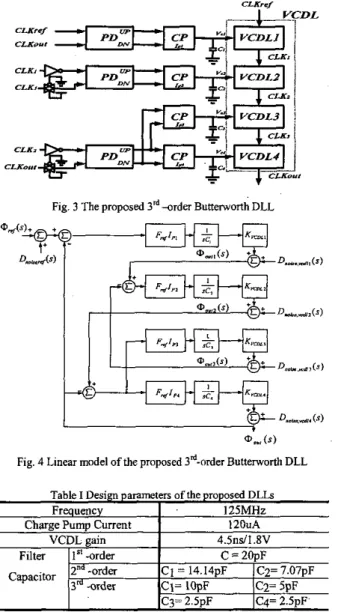
Butterworth DLL could be also shown in Fig. 3. The 3'd-order Butterworth DLL consists of four loops. The VCDL, which is the same one in the conventional DLL, can be divided into 4 equal delay sections. The first phase detector is used to compare the phase between CLKref and CLKouf as the conventional DLLs did. The second phase detector is used to detect the phase error between CLKI and CLK3, while the third phase detector is used to detect the phase error between CLK2 and CLKout. Fig. 4 is the linear model of the proposed 3"-order Butterworth DLL. The transfer function
of
the 3"-order Butterworth DLL can be derived asFrequencv
Charge Pump Current
VCDL gain Filter 1" -order
Capacitor 2"' -order
3* -order
1
,where
WNt
=
Fr41piKvd,i
- for i=I-4. Assume theci
125MHz l2OuA 4.5nd1.8V C = 20pF C 1 = 14.14pF IC2=7.07pF CI= lOpF (C2= 5pF C3= 2.SpF Ic4= 2 . 5 ~ ~gain of the third loop and the fourth one are the same, i.e.
wN, =wN,
.
To meet the 3"-order Butterworthpolynomial,
s3
+2w,s2
+
2w,
s+
wf
, the coefficients of the denominator in eqn. (4) should be2
2 3
1 ( 5 )
W N , : WN, : WN, : WN, : wc =-: 1 : 2 : 2 : 1
To have the same comer frequency as the conventional DLL, the cauacitors' rel2ion could be exuressed as
,where C i s the capacitor used in the conventional DLL. The parameters of the proposed DLLs are listed in Table I.
Unlike to use a higher-order loop filter to achieve a higher-order system, the proposed Butterworth DLLs do not have the stability considerations. Since the loop behavior of the proposed DLLs is the same as the higher-order Butterworth lowpass filter, the loop is stable. In addition, using a higher-order loop filter can only suppress the jitter caused by the input nose. However, the proposed Butterworth DLLs can reduce both the jitters generated by the input noise and the VCDL noise.
111. Jitter analysis of the proposed Butterworth DLLs
Assume that the input noise, Dnoisc,mdf),
is
a stationary Gaussian band-limited noise with a null mean value and a uniform spectral dimityNo,p'A,et (PIHZ) in the frequency band (-B/2, +B/2). The output jitter,Dou.,@,
due to input noise is thus a stationary Gaussian noise with a null mean value and a power spectral density S,,,Xf)(f/Hz)
from -B/2 to +B/2.. The standard deviation due to input noise can be derived as,
Fig. 3 The proposed 3"4rder Butteworth DLL
,where Href(j
.
f) is the input noise transfer function.Similarly, the standard deviation due to the VCDL noise can also be derived as
nvcd2
, where h'O.vcdl/Awd~
(f%)
is the spectral density of VCDL noise and Hvcdl(i.
f ) is the VCDL noise transfer function, respectively. Thus, the total output noise can be expressed asAssume and the interested noise
2
Is,,
' d f = N x d l - BAcdi
bandwidth is much larger than the comer frequency of the noise transfer function, i.e. B >> f,, the total output noise of the conventional DLL can be given as
2
(10)
Daw.m~,-
n px .rc
+ N,* . BA
ref,where
f,
is the comer frequency. The first term is proportional to the loop bandwidth of the DLL. The second term is independent of the loop bandwidth. The results are the same as that analyzed in[I].
Since the output noise contributed by each VCDL in the 2"d Butterworth DLL is identical and half of that of
conventional DLL, i.e. N ~ ~ , , = N ~= z ~ v c d , ~ ,
,
~the totaloutput noise of the Znd-order Butterworth DLL can be given as
1
Similarly, the output noise contributed by every VCDL in the 3'-order Butterworth DLL is identical and it is equal to one-fourth of the VCDL in the conventional DLL, i.e. N ~ , , = N , , = N,,, = N , ~ , , = $ N , ~ , . The total output noise of the 3" Butterworth DLL can be given as
From eqns.(l0)-(12), given the same comer frequency,
A,
the proposed Butterworth 2"d-order DLL and 3'-order one can improve the jitter performance due to input noise by a factor of andfi,
respectively, and improve the jitter preformance due to VCDL noise by a factor of&
and 2, respectively.W . Circuit description
In order to compare the performances of the conventional D1.L and the proposed DLLs, the building blocks, such as the VCDL, the phase detector, and the charge pump circuit, are identical and their relative layout positions are also the same. They are described as follows:
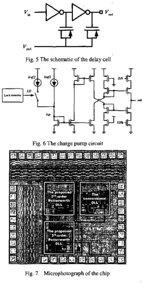
A . Voltage-controlled Delay Cell
The schematic of the delay cell used in this work is depicted in Fig.
5 .
It is composed of two identical inverters loaded with PMOS voltage-controlled varactors which can be immune from the suhstrate noise in a N-well process. The duty cycle distomon will become worse when many delaycells are caccaded to realize a VCDI. with a relatively large
delay time. From this point of view, the analog delay cell in Fig. 5 possesses a highly s y m m e ~ c a l property. For
example, rising clock edge encounters a falling transition followed by a rising transition while passing the delay cell.
On the other hand, a falling clock edge encounters a rising transition followed by a falling transition while passing the delay cell. Both of them are delayed by the amount of one rising-edge delay time plus one falling-edge delay time except that the sequence is different. Therefore, they are almost delayed by the same delay time. This helps to preserve the clock duty cycle when a VCDL with a relatively large delay time is used.
B. Charge Pump
The charge pump circuit is shown in Fig. 6. A technique called dynamic bandwidth-adjusting scheme (DBAS) is adopted here to shorten the lock time without compromising the jitter performance. The reference current, Icp. has two current sources, one is normally tumed on, and the other is controlled by a lock detector
(LO).
When the loop is unlocked, LD is low and makes the bias current almost.Fig. 5 The schemtic of the delay cell
T T T r - r T
Fig. 6 The charge pump circuit
Fig. 7 Microphotograph of the chip
(3) The conventional DLI
-
- 5-
.*.""
... ... . . .~... ~ . . . . .~. . .I::
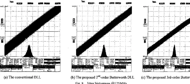
@)The proposed 2"40rder Bunerworth DLL (c) The proposed 3rd-order Bunerworth DLL Fig. 8 Jitter histograms @125MHz
doubled and it will widen the loop bandwidth to shorten the lock time. When the phase error is smaller than the lock window defined by the lock detector [2], LD goes High and narrow the loop bandwidth to improve the jitter performance.
C. Phase detector
to overcome the speed limitation and reduce the dead zone.
In this work, the dynamic logic style PFD [3] is adopted
V. Experimental results
Three DLLs have been fabricated at the same die in a 0.35um CMOS process as shown in Fig. 7 and the whole chip area is 1.44 including
U 0
pads. Assume the gain of the third loop and the fourth one are the same in the 3d-order Bunerworth DLL, the contol voltage of the third loop can be substituted by that of the fourth loop. Hence, the charge pump circuit and loop filter of the third loop can be omitted in Fig.3. Fig. 8 gives the measured jitter histograms. The measured peak-to-peak jitter of the conventional, the 2"d-order, and the 3rborder DLLs is 51.6ps, 40.Ops and 29.2ps, respectively, with the input frequency of 125MHz. The measured rms jitter of the conventional, the 2"d-order, and the 3'40rder DLLs is 7.34ps, 5 . 2 4 ~ s and 3.75ps, respectively. Compared with the conventional DLL, the measured ms jitters of the proposed DLLs can be improved by a factor of1.40 and 1.95. If the most part of the output noise is mainly conbibuted by the VCDL and the input noise can be filtered by narrowing the loop bandwidth, the measured results are close to the analysis discussed above. The performance summary is listed in Table 11.
I .47 mm
VI. Conclusion
In this paper, the proposed Buttenvolth DLLs can improve the jitters without stability considerations. Compared to the conventional DLL, the proposed Butterworth 2"d-order
DLL and the 3d-order one could reduce the noise due to VCDL by a factor of
&
and 2, repectively. In addition, the dynamic bandwidth adjusting scheme is also introduced in the proposed DLLs to achieve the shorter lock time without compromising with the jitter performance. The measured results also demonstrate the functionality of the proposed DLLs.Acknowledgement
The authors would like to thank National Chip Implementation Center, Taiwan, for chip implementation.
Table I1 Performa Process Supply Voltage Frequency Range Power Consumption PkPk jitter r.m.s. jittei
: summary of the proposed DLLs
0 35-um 1P4M CMOS process 3 .0-3.6V 100-140MHz 32mW @ 125MHz, 3.3V 51.6ps@ 15'order, 125MHz 4 0 . 0 ~ s @ 2"' order, 125MHz 29.2~s @ 3m order, 125MHz 7 . 3 4 ~ 8 @ ls'order, 125MHz 5.24~s @ 2"d order, 125MHz 3 . 7 5 ~ s @ 3" order, 125MHz Chip Area
I
1 . 4 4 ~ 1 . 4 7 " l@withI/OpadsReferences
I. J . Kim, S. B. Lee, T. S. lung, C. H. Kim, S. I. Cho, and B. Kim," A
low-jiner mixedmade DLL for high-speed DRAM applicatian,"lEEE J Solid-Slate Cirmitr, vol. 35, no. 10, pp. 1430-1436, Oct. 2000.
G . K. Dehng, 1. M. Hsu, C. Y. Yang, and S. I. Liu, "Clockdeeskew
buffer using a SARionlrolled delay-locked Imp", IEEE J. Solidstole
C i m i l r , vol. 35, no. 8, pp. 1128-1 136, Aug. 2000.
S. Kim, K. Lee, Y . Moon, D. K. Jeong, Y. Choi and H. K. Lim, "A
960-Mb/s/pin interface far skew-tolerant bus using low jitter PLL,"
IEEEJ Solid-Store Circuilr, vol. 3 2 , no. 5, pp. 691-700, May 1997.