國
立
交
通
大
學
電子工程學系 電子研究所
博 士 論 文
系統資料頻寬之研究
Study on System Data Bandwidth for Video and Vision Applications
研 究 生:張彥中
指導教授:張添烜 教授
王聖智 教授
系統資料頻寬之研究
Study on System Data Bandwidth for Video and Vision Applications
研 究 生:張彥中 Student:Nelson Yen-Chung Chang
指導教授:張添烜 Advisor:Tian-Sheuan Chang
王聖智 Sheng-Jyh Wang
國 立 交 通 大 學
電子工程學系 電子研究所
博 士 論 文
A DissertationSubmitted to Department of Electronics Engineering and Institute of Electronics
College of Electrical and Computer Engineering National Chiao Tung University
in partial Fulfillment of the Requirements for the Degree of
Doctor of Philosophy in
Electronics Engineering August 2009
Hsinchu, Taiwan, Republic of China
系統資料頻寬之研究
研究生:張彥中 指導教授:張添烜 博士
王聖智 博士
國 立 交 通 大 學
電機學院 電子工程學系 電子研究所
摘
要
資料頻寬問題長久以來就是嵌入式系統效能的瓶頸。若一個系統無法提供足夠的資 料頻寬,或運算核心的頻寬需求過高,會造成運算核心缺乏足夠運算資料,因而使運算 核心無法發揮全部的運算能力,進而影響到系統的效能。為了發揮系統的效能,本論文 探討如何提高系統中可用頻寬使用率與降低頻寬需求。本論文以系統中資料傳輸的過程 為主軸,針對傳輸源頭到終端所會遭遇的頻寬問題進行改善的研究。改善方法的核心概 念是利用傳輸或存取資料之間的相關性,搭配系統中硬體裝置的工作特性提高頻寬使用 率,或是重複利用已有資料減少頻寬需求。在資料傳輸的源頭,也就是記憶體控制器的 部份,本論文探討如何透過存取排程,改善資料間的相關性,利用記憶體本身存取特性 與系統匯流排協定的工作特性來提高的資料頻寬使用率。在改善資料傳輸源頭的頻寬 後,瓶頸便落在系統匯流排上,因此本論文接著探討改善採用先進封包式協定匯流排頻 寬使用率的方法。在資料傳輸末端的運算核心部份,本論文則是根據資料間存取的空間 與時間的相關性,探討如何透過有效地資料重複使用,降低運算核心的頻寬需求。本論 文研究的運算核心功能包含了視訊編解碼與早期視覺處理,這兩類運算的頻寬需求皆十 分可觀。在視訊編解碼部份,本論文針對移動補償提出了一利用輸入移動向量與巨方塊 種類之內容特性的運算核心硬體架構,可降低頻寬需求達72%。而在早期視覺處理部 份,本論文針對平均飄移濾波演算法與立體視覺的立體匹配演算法,提出可減低頻寬需 求的運算核心硬體架構。在平均飄移濾波架構中,本論文根據平均飄移向量大小的特性,提出部分更新乒乓暫存記憶體架構,可減少八成畫面記憶體頻寬需求。另一方面, 在立體匹配演算法中,本論文根據演算法本身資料存取在空間與時間上的侷限性與相關 性,提出部份列資料重複使用與擴張視窗減少存取兩方法,來達到大幅減少立體匹配資 料頻寬需求。本論文基於資料相關性的頻寬改善方法,可提高可用頻寬與降低頻寬需 求,有效改善系統中資料頻寬的問題,進而幫助提高系統整體效能。
Abstract
Data bandwidth issue has long been the performance bottleneck of an embedded system. The computation cores in a system cannot maximize their utilization without enough data. This is usually a result of insufficient available data bandwidth or excessive data bandwidth requirement. Being aware of the importance of the data bandwidth issue, this dissertation addressed the bandwidth issue from the source to the destination of data transfers. The core concept was to facilitate the address and data correlation among accesses to solve the data bandwidth issue. Exploiting these correlations can increase bandwidth utilization given a device’s access characteristics and can also reduce bandwidth requirement through data reuse. In particular, this dissertation explored methods to increase the bandwidth utilization of memory controllers by taking the advantage of the characteristics of external memories and new advanced data transfer protocol. After improving the bandwidth utilization at the source of data transfers, this dissertation focused on improving the bandwidth utilization of a bus interconnect adopting advanced protocol under the traditional share-link topology. Finally, bandwidth requirement reduction techniques have been studied at the destination of data transfers. For video coding and early vision tasks, these techniques performed data reuse based on algorithm’s data access characteristics, such as the spatial ad temporal locality among data accesses. In video coding, this dissertation proposed a combined frame memory motion compensation (CFMMC) architecture that was capable of reducing the bandwidth requirement by up to 72% based on the characteristics of input motion vector and macroblock type data. In early vision tasks, this dissertation proposed a meanshift filtering architecture that used the proposed partial-update ping-pong buffer (PUPPB), which was based on the access locality due to intermediate meanshift vector characteristics, to reduce the bandwidth
to the image memory by 81.6%. In stereo matching vision task, this dissertation proposed the partial column reuse (PCR) and access reduction by expanding window (AREW) techniques, which were based on the access locality due to the algorithm’s flow, to significantly reduce bandwidth requirement for the proposed mini-census adaptive support weight (MCADSW) stereo matching architecture. The bandwidth utilization improving and bandwidth requirement reduction techniques studied in this dissertation can also be applied to other video coding or vision systems to improve system performance.
誌
謝
博士的研究生涯,得到了不少人的幫助。首先要感謝任建威博士,在我的碩士和博 士初期給予的指導,同時感謝他提供良好的研究環境和資源。另外要感謝我的指導老師 張添烜教授與王聖智教授,在我博士班期間毫無保留指導與建議。我要特別感謝張教授 鼓勵我朝自己夢想與有興趣的題目進行研究,同時也要感謝王教授願意給我在這方面幫 助,讓我受益良多。沒有這兩位教授的幫忙,我今天將不會有實現我自己的夢想的機會。 另外,也要感謝我的口試委員:李鎮宜教授、蔡淳仁教授、楊家輝教授、張寶基教授、 陳永昌教授、陳紹基教授、蔣迪豪博士,在忙碌中抽空齊聚ㄧ堂,參與我的論文口試, 並給予十分有幫助的建議,讓我獲益良多。 另外,我也要感謝我的家人。首先,我要感謝我的父母,沒有你們的不間斷的督促 與鼓勵,我將無法在論文連續被拒絕時,重新站起來。也要感謝父親,能夠理解並接受 我改變研究方向。也要謝謝父母給我一個能後放心追求夢想的家庭。此外,也要感謝兄 弟們(這包含友然在內)在博士班其間給我的鼓勵。 最後,要感謝在交大這幾年相遇的學長、同學、學弟妹們。首先要感謝李坤儐學長 的用心帶領和指導,另外也要感謝林泰吉學長和李元仲學長願意適時給予有用的意見。 同時還要感謝博士班重逢的林佑昆同學和約旦來的Esam同學,在這幾年間相互鼓勵, 一起努力。接著要感謝和我一起合作的學弟妹們:浩雲、惠錚、旻奇、宗憲、宇晟、景 竹。最後,要感謝張教授實驗室全體學弟妹,謝謝你們這段期間帶來的歡笑和幫忙。最 後,也要謝謝我所有的朋友的鼓勵與幫忙。 謹將這本論文,獻給所有關心我的人們,也獻給不幸離開人世的蔡旻奇學弟。Contents
摘 要 ...i
Abstract ...iii
誌 謝 ... v
Contents...vii
List of Figures ...ix
List of Tables...xi
Chapter 1 Introduction ... 2
1.1. Background... 2
1.2. Motivation... 3
1.3. Dissertation Organization ... 4
Chapter 2 Related Works ... 6
2.1. Memory Controller ... 6
2.2. System Bus ... 7
2.3. ASIP Data reuse related ... 11
2.3.1. Motion Compensation in Video Codecs ... 11
2.3.2. Meanshift Filtering in Segmentation... 12
2.3.3. Stereo Matching ... 14
Chapter 3 AXI Memory Controller ... 18
3.1. Memory Controller's Role in a System ... 18
3.2. DRAM Basics ... 19
3.3. AXI Memory Controller Policy ... 21
3.3.1. Overall Scheduling Framework ... 21
3.3.2. First-level: Transaction-Level Scheduling... 21
3.3.3. Second-Level: Command Scheduling... 23
3.4. Simulation Result... 24
3.4.1. Multimedia Platform Architecture ... 24
3.4.2. Videophone Application ... 25
3.5. Simulation Result... 26
3.5.1. Evaluation Metrics ... 26
3.5.2. Burst Length Impact... 27
3.5.3. Transaction Buffer Size Impact ... 29
3.5.4. Bus Arbitration Policy Impact... 32
3.6. AXI Memory Controller Architecture ... 33
3.7. Summary... 34
Chapter 4 AXI Shared-link Bus ... 36
4.1. System Bus' Role in a System... 36
4.2. Proposed AXI Scheme... 38
4.2.1. Transfer Modes ... 38
4.2.2. Arbitration Scheme... 41
4.3. Simulation Setup... 43
4.3.1. Multimedia Platform Architecture ... 44
4.3.2. Video Phone Scenario ... 45
4.3.3. Evaluation Metrics ... 46
4.4.1. AXI Interface Buffer Size and Bus Arbitration Impact... 48
4.4.2. Task Access Setting Impact ... 52
4.4.3. Single-Layer Shared-link AXI vs. 5-Layer AHB-lite ... 54
4.5. Summary... 56
Chapter 5 Bandwidth Reduction Techniques in Computation Cores... 58
5.1. Bandwidth Reduction Methods... 58
5.2. CFMMC... 59
5.2.1. Motion Compensation's Role in a Video Decoder System ... 59
5.2.2. Combined Frame Memory Motion Compensation ... 61
5.2.3. Architecture... 71
5.2.4. Implementation Result... 80
5.2.5. Summary... 84
5.3. Meanshift ... 86
5.3.1. Meanshift's Role in Vision Applications... 86
5.3.2. Meanshift Algorithm... 87
5.3.3. Test Images and Mean Shift Filter Parameter Settings... 89
5.3.4. Meanshift Architecture... 90
5.3.5. Implementation result... 102
5.3.6. Summary... 104
5.4. MCADSW ... 105
5.4.1. Stereo Matching's Role in Vision Applications ... 105
5.4.2. Stereo Matching Issues ... 105
5.4.3. MCADSW algorithm ... 106
5.4.4. Bandwidth Reduction Techniques for MCADSW Architecture ... 114
5.4.5. Real-time Architecture for MCADSW ... 118
5.4.6. Implementation Result and Comparison ... 124
5.4.7. Summary... 128
Chapter 6 Conclusion... 130
List of Figures
Fig. 1. Simplified block diagram of a DRAM ...19
Fig. 2. Bank state transition and related commands when (a) current bank state is idle (b) current bank state is active and row-hit (c) current bank state is active and row-miss...20
Fig. 3. Overview of the two-level scheduling flow ...21
Fig. 4. The target platform ...24
Fig. 5. Bandwidth usage of different memory scheduling policies with (a)FP and (b)RR bus arbitration ...27
Fig. 6. Power consumption of different memory scheduling policies with (a)FP and (b)RR bus arbitration ...28
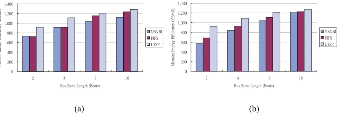
Fig. 7. Memory energy efficiency of different memory scheduling policies with (a)FP and (b)RR bus arbitration...29
Fig. 8. Bandwidth usage of different buffer size with (a)FP and (b)RR bus arbitration ..30
Fig. 9. Memory power consumption of different buffer size with (a)FP and (b)RR bus arbitration...31
Fig. 10. Memory energy efficiency of different buffer size with (a)FP and (b)RR bus arbitration...31
Fig. 11. Architecture of the AXI-compatible memory controller with the two-level scheduling policy ...33
Fig. 12. Normal mode transfer example ...39
Fig. 13. Interleaved mode transfer example...39
Fig. 14. Data locked mode transfer example ...40
Fig. 15. Arbitration framework for a share-link AXI bus...42
Fig. 16. Block diagram of the target platform using (a)AXI, (b) AHB-lite...45
Fig. 17. Performance of different interface buffer size and arbitration policy combinations ...50
Fig. 18. Performance of different task access settings and interface buffer size ...53
Fig. 19. Performance of 5-layer AHB-lite and single-layer shared-link AXI ...55
Fig. 20. Impact of different QP values on percentage of NOT-CODED MB in MPEG-4 ...63
Fig. 21. Memory components for QCIF with vector range of [-16:+15] in the CFM ...64
Fig. 22. Flow chart of motion compensation process in the CFMMC ...65
Fig. 23. The processing of non-perfect-matched MBs ...66
Fig. 24. Life time analysis of MBs ...67
Fig. 25. Block diagram of the CFMMC hardware...73
Fig. 26. Pblk offsets and inblk offsets...73
Fig. 27. Block diagram of the memory accessor ...75
Fig. 28. Gate count distribution and comparison of the logics part in the PPFMMC and the CFMMC...81
Fig. 29. Plot of the energy reduction percentages of the CFMMC at different P0...82
Fig. 30. Power consumption distribution and comparison of the PPFMMC and the CFMMC...83
Fig. 31. Power consumption distribution and comparison of the PPFMMC and the CFMMC for mobile and akiyo. ...84
Fig. 33. Block diagram of the proposed Meanshift filter architecture...91
Fig. 34. Concept of PUPP reuse...93
Fig. 35. Block diagram of PUPP...94
Fig. 36. Image memory pixel read count comparison between using PUPP and not using PUPP ...96
Fig. 37. Block diagram of the PPLMSSB...98
Fig. 38. Datapath and pipeline schedule of the MSVCU...99
Fig. 39. Block diagram of the SML ...101
Fig. 40. Processing cycles and estimated frame rate of each test images...102
Fig. 41. Overall flow of the proposed mini-census adaptive support weight algorithm.106 Fig. 42. The census transform and matching ...107
Fig. 43. Disparity estimation error rate of using different color spaces ...109
Fig. 44. Scaled, truncated, and non-zero MSB preserved weight function ...110
Fig. 45. Partial column reuse in mini-census transform ...114
Fig. 46. Partial column reuse in cost aggregation...115
Fig. 47. Example of access count reduction with expanded window, (a) without expanded rows, (b) with 3 expanded rows...117
Fig. 48. Block diagram of the MCADSW ...118
Fig. 49. Architecture of the mini-census transformer ...119
Fig. 50. Architecture of the weight generator ...120
Fig. 51. Architecture of the cost aggregator and WTA...121
Fig. 52. Schedule of the ping-pong buffer ...122
Fig. 53. Processing schedule of the cost aggregator ...122
Fig. 54. Schedule of the MCADSW architecture ...123
List of Tables
Table 1 The task, access pattern, bandwidth, and completion time requirement of each
master device ...25
Table 2 Performance evaluation metrics...27
Table 3 Port task description and bandwidth requirement...46
Table 4 Combinations of arbitration policies...48
Table 5 Weight allocation of TDMA and Lottery arbitration schemes ...48
Table 6 Task access settings ...52
Table 7 Percentage of perfect-matched MBs when QP=16...62
Table 8 Memory sizes required in CFM ...68
Table 9 Memory access energy consumption and access latency of processing one frame ...69
Table 10 Average memory access energy consumptions and latencies for various QCIF test sequences with k=4 ...69
Table 11 Latencies of different MB modes ...79
Table 12 Energy reduction percentage of the real test patterns ...83
Table 13 EDISON’s execution time of VGA image “Raincoat Sam” on a PC with PentiumIV 2.8GHz processor and 1GB memory. ...86
Table 14 Synthesized gate count of each component ...102
Table 15 Comparison of existing segmentation implementation ...103
Table 16 Performance comparison between using Euclidean and Manhattan color distances...110
Table 17 Performance comparison of the MCADSW and other algorithms ...113
Table 18 Core characteristics of the proposed MCADSW...124
Table 19 Speed comparison of different implementations ...125
Chapter 1 Introduction
1.1.
Background
Video coding technology has been developed over the past four decades and has made high quality portable video playback and recording a reality. Examples of portable video playback include the early suitcase TV [1], recent portable media players [2], and newly available iPhones [3]. On the other hand, portable video recording has also been developed after Le Prince invented moving picture recording technology since 1890’s. Now, portable video recording can be found on small handheld camcoders to cell phones. These have been possible because of the advances in digital video coding algorithms, which have greatly improved the compression ratio while maintained high video quality. However, advanced digital video coding algorithms are often complex and computation power demanding.
Recently, real-time and portable vision-based applications have been receiving great attention. Vision algorithms, particularly early vision ones, have enabled traditional image/video consumer electronics to become smarter than ever. For instance, face detection and region of interest have improved a camera’s focus capability [4] and made a camera seem “smarter” to human users. In addition to traditional image/video consumer electronics, vision algorithms have also been the core technology in robotics, autonomous vehicles, and intelligent surveillance. However, the drawback of using vision algorithms was the enormous computation requirement. The complexity of vision algorithms has been much higher than video coding algorithms. As a result, real-time implementations of vision algorithm were not as successful as in video coding technology.
One common approach to accommodate the computation requirement is to use multi-core embedded systems. A multi-core embedded system may include embedded processors, DSPs,
high performance processors, GPUs, and dedicated hardware accelerators to satisfy the computation power requirement of video and vision algorithms. The large computation requirement issue can be easily solved by using a multi-core embedded platform. However, the hard part is the data bandwidth. Without the data to be processed, a computation core can only idle helplessly. Therefore, it is crucial to take care of the data bandwidth issue to ensure an embedded multi-core system works as expected.
1.2.
Motivation
Being aware of the fact that the data bandwidth is one of the key factors that affects the system speed, this work explored methods to improve system speed under limited resource. One way to improve the system speed is to increase the available BW by investing more hardware resource. Examples of such approach were using higher clock rate, wider data port width, more buses, and complex crossbar interconnect. However, this approach often led to expensive systems.
Other approaches that demand less hardware resources were maximizing existing bandwidth utilization and reducing bandwidth requirement. Maximizing bandwidth utilization can be achieved by using new data transfer protocols and access methods. One example of new advanced data transfer protocols was AMBA AXI [7], which adopted a packet-based channel scheme to maximize the bandwidth utilization. Better access methods can increase the bandwidth utilization by taking access device’s characteristics into account.
Reducing bandwidth requirement can be achieved by reusing data within computation cores so that less data transfer and access outside the cores are needed. Such data reuse often depends on finding data access characteristics of algorithms, such as data access spatial and temporal locality. Another approach in reducing bandwidth was by compressing the data to
be transferred. However, this approach often introduced additional compression hardware. Hence compression-based methods were not discussed within the scope of this dissertation.
Motivated by the importance of bandwidth issue and the potential opportunities of the aforementioned approaches on maximizing bandwidth and reducing requirement, this work focused on the study of facilitating the features of new data transfer protocols and intrinsic characteristics of memory devices and algorithms to improve system performance. In this dissertation, the bandwidth bottlenecks in a multi-core embedded system were investigated from the source to the destination of data flow. In particular, the bandwidth issue at a memory controller, a system bus, and application specific cores were studied.
1.3.
Dissertation Organization
The first chapter gave a brief introduction on the background, motivation, and the organization of this dissertation. The second chapter presented previous arts and related literatures to help readers better understand the detail background of this dissertation. Chapter 3 presented our study on the bandwidth issue at the source of data transfer, the memory controller. We have presented a method to improve the bandwidth utilization taking the advantage of the memory device’s intrinsic characteristics as well as the new bus protocol’s feature. Once the bandwidth performance at the source is improved, the system bus would become the data transfer bottleneck. Therefore Chapter 4 analyzed the bus bandwidth issue at system level and provided methods of enhancing the system bus performance by facilitating the features of new bus protocols. Chapter 5 studied the bandwidth issues at the destination of data transfers, the application specific computation cores. Finally, Chapter 6 gave a conclusion and some future work directions.
Chapter 2 Related Works
Related works were categorized into memory controller related, data transfer related, and application specific computation core related. In the memory controller part, previous works on DRAM memory controllers were presented. In the data transfer part, researches on analyzing and improving the bandwidth issue on system bus were described. Finally, in the application specific core part, we investigated previous work on motion compensation in video coding, mean-shift filtering, and stereo vision.
2.1.
Memory Controller
Several works have been proposed to improve DRAM performance on bandwidth utilization and latency. It was initially discussed for single core environment with software based techniques to reorder access streams [8]. Instead of software approach, Ayukawa et al. proposed an access-sequence controller [9] which reorders the data input and output order to reduce access latency. However, neither transaction nor command scheduling were mentioned in their work. Later, Rixner et al. proposed a memory access scheduler architecture [10] capable of adopting various combinations of simple DRAM command arbitration policies and can perform bank-interleaving. In these works, they only focused on single core environment and neglected the impact of the arbitration policy on system buses.
For multicore environment, Takizawa et al. proposed a simple memory arbitration policy which reduces bank conflict and read/write turnaround in their MPEG-2 AV decoder system [11]. However, reducing bank conflict by increasing bank-interleaving would result in row precharge and activation increase, thereby increasing the memory power consumption. Recently, Lee et al. proposed an efficient quality-aware memory controller for multimedia
platform SoC [12]. It utilizes a quality-aware scheduler to provide quality-of-service (QoS) guarantees. However, their scheduler requires multiple channels which may only be suitable for systems adopting star topology and will result in extra hardware cost for the system.
In the industry, Rambus proposed a pipelined memory controller [13] which includes a bank cache lookup and a command sequencer. Sonics Limited developed MemMax 2.0 memory controller [14] which improves the efficiency of DRAM but must be used their own MicroNetwork on-chip bus standard. For packet-based bus systems, ARM Limited has developed a configurable AXI compliant memory controller [15].
Despite improving bandwidth utilization and access latency, reducing memory energy consumption has also been discussed at system level [16][17][18]. These works essentially turn DRAMs into low power state during idle period by using either software or hardware approaches. However, reducing memory energy consumption in non-idle period should also be addressed to further reduce the system energy consumption. Meanwhile, the system timing constraint must also be met. Such issue has been briefly discussed in Burchardt’s work [19]. However, thorough investigation on improving memory energy efficiency in non-idle period still remains rare.
2.2.
System Bus
With the rapid progress of system-on-a-chip (SOC) and massive data movement requirement, on-chip system bus becomes the central role in determining the performance of a SOC. Two types of on-chip bus have been widely used in current designs, which are pipelined-based and packet-based bus.
For pipelined-based buses, such as ARM’s AMBA 2.0 AHB [23], IBM’s CoreConnect [24], and OpenCore’s WishBone [25], the cost and complexity to bridge the communications among on-chip designs are low. However, pipeline-based bus suffers from bus contention and
inherent blocking characteristics due to the protocol. The contention issue can be alleviated by adopting multilayer bus structure [26] or using proper arbitration policies [27][28]. However, the blocking characteristic, which allows a transfer to complete only if the previous transfer has completed, cannot be altered without changing the bus protocol. This blocking characteristic reduces the bus bandwidth utilization when accessing long latency devices, such as an external memory controller.
To cope with the issues of pipelined-based buses, packet-based buses such as ARM AMBA 3.0 AXI [7], OCP-IP’s Open Core Protocol (OCP) [30], and STMicroelectronics STBus [31] have been proposed to support outstanding transfer and out-of-order transfer completion. We will focus on AXI here because of its popularity. AXI bus possesses multiple independent channels to support multiple simultaneous address and data streams. Besides, AXI also supports improved burst operation, register slicing with registered input, and secured transfer.
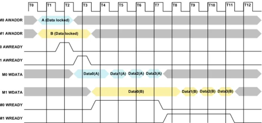
Despite the above features, AXI requires high cost and possesses long transaction handshaking latency. However, a shared-link AXI interconnect can provide good performance while requiring less than half of the hardware required by a crossbar AXI implementation. This work focused on the performance analysis of a shared-link AXI. The handshaking latency is at least two cycles if the interface or interconnect are designed with registered input. This would limit the bandwidth utilization to less than 50%. To reduce the handshaking latency, we proposed a hybrid data locked transfer mode. Unlike the lock transfer in [32] which requires arbitration lock over transactions, our data locked mode is based on a transfer-level arbitration scheme and allows bus ownership to change between transactions. This gives more flexibility to arbitration policy selection.
With the additional features of AXI, new factors that affect the bus performance are also introduced. The first factor is the arbitration combination. The multi-channel architecture
allows different and independent arbitration policies to be adopted by each channel. However, Existing AXI related works often assumed a unified arbitration policy where each channel adopts the same arbitration policy [32][33][34]. Another key factor is the interface buffer size. A larger interface buffer usually implies more out-of-order transactions can be handled. The third factor is the task access setting, which defines how the transfer modes should be used by the devices within a system. Proper task access settings can yield better performance. However, the proper setting may be different under different circumstances, such as different buffer sizes.
Many works have been conducted on the communication architecture of pipelined-based bus. Earlier work used formal analytic approach [35][36] to explore the design space of communication architecture to evaluate the performance of a pipeline-based bus system. Although formal analytic approach can provide the average or best/worst case overall bus performance, such approach can hardly account for instantaneous changes of bus behavior. This limitation gave rise to high-level simulation-based approach which is capable of capturing the detailed instantaneous bus behavior with cycle accuracy [37]. Pasricha et al. [38] used the cycle count accurate transaction boundaries (CCATB) model in the architecture exploration of an MPEG AHB system. Later, Pasricha et al. also conducted experiment on bus architecture synthesis [39] under different given constraint. Their synthesis method yielded cost efficient bus matrices much faster and reliable than manual optimization.
Most of the techniques developed in the abovementioned works can be extended for the analysis of packet-based bus. Pasricha et al. extended their communication architecture synthesis framework to AXI [34]. Their work automatically generates the best bus topology, arbitration policy, and parameter settings driven by throughput requirements. Besides bus topology exploration, comparison between packet-based bus and pipelined bus has also drawn attention. Pasricha et al. [40] compared the performance of a shared-link AXI and a
single-layered AHB. Their comparison showed that up to 30% of bandwidth utilization improvement can be achieved by AXI compared with AHB. They also investigated the impact of the transaction reordering buffer size in the memory controller. Lee et al. [41] built a crossbar AXI platform and a single-layered shared-link AHB platform to quantify the performance difference. They reported 40% communication efficiency improvement between AXI and AHB. Ruggiero et al. [42] studied the scalability of AHB, AXI, and STBus under shared bus topology. Their result showed that AXI is far more scalable to the number of master devices than AHB. When the number of processor reaches 8, AXI can achieve 60% bandwidth utilization improvement over AHB.
Comparison of bus connectivity configuration, such as shared-link, multilayer (partial crossbar), and full matrix (crossbar), has also been interested as well. Lahiri et al. [43] proposed a design space exploration methodology and compared the performance between single-layer and multilayer shared-link buses. Recently, Murali et al. [44] presented a bus communication architecture exploration method that finds the most power-efficient crossbar interconnect for a packet-based bus. They also briefly compared the performance and normalized cost ratio among shared-link, multilayer, and crossbar configurations.
Although the aforementioned works conducted analyses on communication architecture, the register slicing impact and multi-channel arbitration issues that arise with the features of packet-based bus have been overlooked. In addition, pervious performance comparison of multi-channel AXI and single-layer share-link AHB may not be fair since AXI requires much more hardware cost.
2.3.
ASIP Data reuse related
2.3.1.
Motion Compensation in Video Codecs
Motion compensation has been one of the most important tasks in a video encoder or decoder. Motion compensation reconstructs a predicted frame from reading frame data from a frame buffer. The reconstructed frame is written back into the frame memory. In many cases, the bandwidth requirement and size of the frame memory is usually large. To reduce the size of the frame memory in motion compensation, [48][49][50] adopted a merged-frame approach which stored the reference frame and the reconstructed frame together using one frame memory with the size slightly larger than one frame. Along with the reduced size frame memory and local buffers, these work claimed that the merged-frame approach is also capable of reducing the power consumption. Among these works, [48] and [49] proposed an in-place storage optimization for video decoders. The in-place storage used a buffer to store the reference frame data that are overlapped with the reconstructed current frame data in a snake-like manner. To handle the complex address generation and the control, they implemented a prototype using software. [50] also proposed a similar merged-frame memory architecture for motion estimation and compensation in an encoder. Although these works successfully reduced the frame memory size, none of them mentioned further improving the performance of motion compensation by exploiting the characteristic of MBs without motion and residue. Consequently, the bandwidth requirement could not be reduced.
Moshnyaga’s works [47][51] on motion estimation reported the presence of block-data whose content remain unchanged between the adjacent frames. These unchanged block-data are facilitated to eliminate frame memory writes and computations during the motion estimation. In order to reduce memory writes for the unchanged block-data, Moshnyga’s work also adopted the merged-frame approach when the coding pattern has no B-frame.
Although the result shown was quite well for the test sequences listed in their works, the experiment result on video sequences with great amount of motion was absent.
2.3.2.
Meanshift Filtering in Segmentation
Several hardware architectures have been proposed to improve the processing speed of image segmentation algorithms. However, very few architectures have been proposed for the Meanshift filter algorithm. For segmentation algorithms other than the Meanshift algorithm, Ranbabu et al. proposed a VLSI architecture for the well-known watershed segmentation algorithm [61]. Their architecture could speed up the speed by 3 times compared to their software implementation. Neuenhahn et al. also implemented the watershed algorithm on an FPGA with optimal parameter settings [62]. Their work could segment 576x720 resolution images at a frame rate of 50 FPS. Yamaoka et al. proposed a VLSI architecture that implemented an image-scan based region-growing segmentation algorithm [63]. The image-scan based region growing algorithm had regular process flow and was therefore more suitable for hardware implementation. Their architecture was capable of segmenting up to 230 segments in QVGA images at a frame rate of 30 FPS.
For clustering-based segmentation algorithms, the K-means algorithm has received great attention by hardware designers. Leeser et al. proposed one of the earliest architecture for K-means color clustering algorithm [64] one decade ago. However, Leeser’s work did not adapt to the characteristics of the image being processed. Maliatski and Yadid-Pecht proposed a hardware-driven architecture for adaptive K-means algorithm [65]. Their architecture was capable of processing with 64 cluster centers in QCIF images at a frame rate of 15 FPS. Later, Hernandez proposed a “global-quasi-systolic local-hyper-connected” VLSI architecture for histogram peak-climbing image segmentation algorithm [66]. Their work could segment images of 702x576 resolution at a maximum frame rate of 50 FPS. However, the cost of Hernandez’ architecture was very large and required a tremendous amount of
internal memories. Maruyama and Saegusa also proposed an architecture for filtered K-means color image segmentation algorithms [67]. They used KD-tree to filter out redundant cluster computations. Their FPGA implementation could perform image segmentation on VGA images at an average frame rate of 35 FPS. However, the maximum segment count in their K-mean implementation was limited to 256. Moreover, the performance of K-means algorithm is heavily dependent on good initial guess of the cluster centers. Recently, Chen et al. presented a design for K-means color segmentation [68]. Their work conducted detailed architectural design space analysis and provided a prototype system that can perform segmentation of QVGA images with a maximum segment count of 16.
In contrast to the attention received by the K-means algorithm, the popular Meanshift clustering algorithm seems to have been over sighted by architecture designers despite the Meanshift’s well recognized performance in image segmentation. Only one architecture has been proposed in the past. Park et al. proposed a systolic array architecture [69] that implemented the dynamic Meanshift (DMS) [70] filter algorithm. The DMS computes a new mode from the old modes in the Meanshift window instead of the original pixel data in the window. The DMS can achieve super-linear convergence and can reduce the execution time by at least 30%. Park et al. modified the DMS to map the modes onto a regular 2-D grid graph to make the computation less irregular. This mapping was suitable for the systolic array architectures and increased the parallelism. To reduce the cost and memory of the array architecture, Park et al. adopted a sliding window approach. However, their DMS architecture would still need a memory to store the mode at each node in the grid graph. If this mode memory is located externally, the bandwidth requirement between the sliding window and the mode memory would be very large.
2.3.3.
Stereo Matching
A. Stereo Matching Algorithms
Disparity estimation algorithms can be categorized into local and global approaches [72]. Local approach determines the disparity of a pixel based on the content similarity between the support windows of this pixel and its candidate pixel in the other image. The local approach usually has low computation complexity and storage requirement, and has been frequently adopted by real-time implementations [74]-[84]. Global approach determines the disparity of all the pixels in an image as a whole by optimizing a global energy function. However, the optimization is usually complex and extremely computation intensive. Hence, we will focus on local approaches.
Early works on local approach studied the impact of different similarity measures [85][86]. Their work pointed out that census, rank [87], and mutual information [88] achieved better disparity estimation performance and were more robust to radiometric distortion. Later, [89] investigated the performance of using different color representation. Recently, [90] investigated the performance and speed jointly of different similarity measure and color representation combinations. The result showed that census-based combination achieved better performance, but also takes more time to compute.
Another important research topic that has been studied is the support window size. The simple fixed size rectangular window adopted in early local approaches suffered from incorrect disparity estimation in occlusion, textureless, and repeating pattern regions. To remedy this, [91][92] proposed variable window size algorithms. Later, [93] also proposed a variable window size algorithm that adaptively adjusted the window size based on a reliability measure. The variable window size could effectively improve the disparity estimation performance in textureless and repeating pattern regions, but not in occlusion regions. Being aware of this, [94][95] proposed shiftable windows algorithms to improve the
performance. Kang et al. [96] combined both the concept of variable window size and shiftable window together. However, the qualitative result of their work still showed great room for improvement.
The reason for not being able to completely improve the performance in the occlusion region is because the assumption of same disparity in the window does not hold in occlusion and slanted surface regions. Understanding this, Veksler [97] proposed a compact window class method which could model non-rectangular support windows. Although their result showed significant performance improvement compared to previous algorithms, the performance near the boundary region was still inferior to complex global approaches. Yoon et al. proposed an adaptive support weight (ADSW) [73] algorithm that assigned different weights to the pixels in a support window based on the proximity and color distances to the center pixel. As a result, the ADSW could achieve the effect of using a support window of arbitrary size and shape. With multiple iterations of aggregations, the performance of ADSW was comparable to some of the complex global algorithms. Later, segmentation-based support methods were also proposed [98][99]. The outlier rejection [98] used a binary weight based on the segmentation region instead of the weight used in the ADSW. Tombari et al.’s segment support algorithm [99] only assign weight to the pixels in the same segment the center pixel is in. Recently, [100] conducted a detailed comparison on the performance and processing speed of local algorithms. Their result showed that the segment support has the highest performance but is two times slower than the ADSW. The performance of the ADSW is only slightly inferior to the segment support algorithm.
B. Real-time Implementations
Real-time stereo matching implementations can be categorized into general purpose processor solutions, digital signal processor (DSP) solutions, graphic processing unit (GPU) solutions, and dedicated hardware solutions.
The general purpose processor solutions rely on the great computation power in state-of-the-art processors to accommodate the high computation complexity of stereo matching algorithms. Early works [76][101] tried to implement real-time stereo matching on general purpose processors, however they could only achieve non-video rate real-time performance due to limited computing power at their times. As the processor technology advances, [102][103][104] implemented real-time stereo matching algorithms on general purpose processors. They managed to achieve real-time processing, but the performance of their disparity map was not very high because of using simple local algorithms. Although simple local algorithms have been adopted by most general purpose solutions, Forstmann et al. [105] proposed a real-time implementation of the less complex global algorithm, the dynamic programming, on general purpose processors. Their performance is higher than most of the previous local algorithms, but their real-time processing speed is limited to images smaller than VGA.
The DSPs have better processing speed on signal processing algorithms because of the SIMD and MIMD architectures than general purpose processors. In addition, they are often less expensive and less power consuming than the state-of-the-art general purpose processors. Hence, DSP solutions are more favorable in embedded stereo vision applications. Konolige’s Small Vision System [76] is one of the most famous early real-time DSP solutions. Recently, [84] also proposed a real-time DSP implementation with jigsaw matching templates. Although the DSP solutions may have more computation power than general purpose processors, the data word alignment and bandwidth issue often limit their capability. As a result, the DSP solutions are usually limited to local algorithms and cannot provide high performance result in real-time.
Another powerful solution is the GPU solutions. The GPUs have extremely high memory bandwidth that ranges from 6.5 GB/sec to 128 GB/sec and can have up to 256
stream processors. With so much hardware resource, the GPU solutions [106]-[109] could implement high performance complex stereo matching algorithms. However, GPUs are too expensive and power consuming to be used in embedded applications currently.
The dedicated hardware solutions can also provide great computation power while allowing the computation resource to be optimized for utilization by designing the architecture in a customized way. This enables the dedicated hardware solutions to be more cost efficient than the GPU solutions. The dedicated hardware includes both FPGA/PLD and applications specific integrated circuit (ASIC). Faugeras et al.’s PeRLe-1 board [110] and Nishihara’s PRISM-3 based stereo system [111] are two of the earliest dedicated hardware solutions. Later, other early dedicated hardware solutions [75][77][78][93] have also been proposed. Among these works, [77] and [78] are two of the first real-time implementation adopting the census matching. However, these early solutions only implemented simple local algorithms. Consequently, their performance is not high. Being aware of the performance limitation of local algorithms, hardware architectures have been proposed for dynamic programming [112] and hierarchical belief propagation (HBP) [113] algorithms [114]. Their performance is very high since they are based high performance global methods. However, their hardware cost is also very high compared to other dedicated hardware implementations. Recently, Tsai et al. [115] studied data reuse techniques in aggregation-based algorithms to reduce the internal storage size, computation resource, and bandwidth requirement.
Chapter 3 AXI Memory Controller
3.1.
Memory Controller's Role in a System
With the rapid progress of VLSI technology, system-on-a-chip (SoC) [1] emerges and becomes feasible with on-chip bus compliant IPs. These SoCs possess sufficient computing power to implement complex and bandwidth demanding multimedia systems for various embedded applications. In such an embedded design, the bandwidth of memory subsystem is one of the major issues that have to be evaluated and optimized first to ensure the system’s success.
We proposed a high bandwidth utilization memory controller which worked with a packet-based bus interface. In which, we have chosen AXI bus [3] as a representing case for packet-based bus that supported flexible out-of-order transaction completion. Packet-based bus not only eliminated the need to access data in request order, the additional transaction ID tag also provided valuable information about the source of an access request that can help in scheduling memory accesses. Thus, we proposed a memory controller with a two-level scheduling framework using such source information. The first level is the transactions-level scheduling which adopts a limited temporal source prioritized (LTSP) policy that used the temporal source correlation of accesses in a system. The second-level was the DRAM command-level scheduling that issues commands based on command age and type to hide access latency. The experimental result of a multimedia platform running a video phone application provided quantitative result of bandwidth usage, memory power consumption, and energy efficiency for different memory scheduling policies.
3.2.
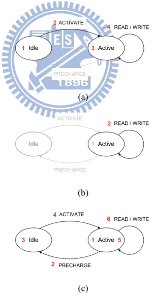
DRAM Basics
Fig. 1 illustrates a simplified block diagram of a DRAM. A DRAM usually consists of four memory banks. For each bank, it includes a row buffer, several memory rows. A DRAM usually has only one data port and is shared for both read and write. The address port is also shared for both read and write.
To access a data located in a DRAM, the row with the data must be first “opened” using an ACTIVATE command. The opened row is read from the memory and written to the row buffer. After the activation, the bank with the row being opened cannot be access for a period of time defined as the active to column access delay. However, other banks can still accept commands. Once the row is opened and the memory bank is ready to accept a command, a column-access READ/WRITE command is issued to access the data in the row buffer. If it is a READ column-access, the data would be available at the data port after a column access latency. Unlike the ACTIVATE command, there can be no other column-access command during the column-access latency because the data port is currently being used. After the current data have been accessed, the memory row can be “closed” by issuing a PRECHARGE command to this bank. Once the row is closed, it would take a period of time called the precharge command period before the next activation command can be issued.
Row De c oder Row De coder Row De cod er Row Buffer Memory row Memory row … Memory row Memory banks Data Port Address Port Row Dec ode r Column Decoder REG REG
Similar to ACTIVATE command, other banks can accept commands within the percharge command period.
Fig. 2 illustrates different DRAM bank state transitions. In Fig. 2(a), if an access happens on an idle bank in which no opened row is available, it is called a bank-miss access. In contrast, if an access happens on an opened row as shown in Fig. 2(b), it is called a row-hit access, which introduces the least access latency. This is because for a row-hit access, only a READ/WRITE column-access command is needed. However, if the access row in an active bank is closed as shown in Fig. 2(c), it is called a row-miss access. For a row-miss access, an additional PRECHARGE command must be issued before the ACTIVATE and READ/WRITE column-access command can be issued. Hence, a row-miss access results in
Idle Active ACTIVATE PRECHARGE READ / WRITE 1 2 3 4 (a) Idle Active ACTIVATE PRECHARGE READ / WRITE 1 2 (b) Idle Active ACTIVATE PRECHARGE READ / WRITE 1 2 3 4 5 6 (c)
Fig. 2. Bank state transition and related commands when (a) current bank state is idle (b) current bank state is active and row-hit (c) current bank state is active and row-miss
the longest access latency.
3.3.
AXI Memory Controller Policy
3.3.1.
Overall Scheduling Framework
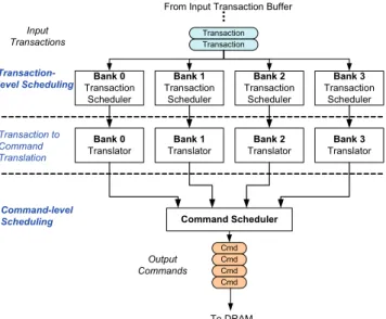
Fig. 3 illustrates the scheduling flow of the proposed two-level scheduling framework. Input transactions are dispatched to each bank for transaction-level scheduling. The goal of transaction-level scheduling is to increase memory row-hit opportunity. After transaction-level scheduling, reordered transactions are translated into DRAM commands with the status of each memory bank taken into consideration. Once the DRAM commands are available, command-level scheduling issues command to DRAM based on command age and the type information. The details of the two-level scheduling are explained as follows.
3.3.2.
First-level: Transaction-Level Scheduling
Two transaction scheduling policies are investigated: first-in first-serve (FIFS) and limited temporal source prioritized (LTSP). The first policy is similar to the first-ready scheduling policy mentioned in Rixner’s work and has been widely adopted. The second one is proposed and recommended in this work. The details of each scheduling policy are described below. Bank 0 Transaction Scheduler Bank 1 Transaction Scheduler Bank 2 Transaction Scheduler Bank 3 Transaction Scheduler Bank 0 Translator Bank 1 Translator Bank 2 Translator Bank 3 Translator Command Scheduler Transaction-level Scheduling Transaction to Command Translation Command-level Scheduling Transaction Transaction ... Cmd Cmd Cmd Cmd Input Transactions Output Commands To DRAM From Input Transaction Buffer
A. Baseline First-In First-Serve
The FIFS policy issues transactions based on transaction input order. The advantage of FIFS policy is its fairness with respect to input transactions because every transaction would eventually be issued. However, FIFS policy is highly dependent on the bus arbitration policy, which determines the transaction input order. This characteristic would make the memory performance sensitive to bus arbitration policy.
B. Limited Temporal Source Prioritized
The proposed LTSP policy sets higher priority to transaction which has the same source as the last issued transaction. In other words, LTSP policy groups transactions from the same source device together. The transactions within a group are issued consecutively based on their relative temporal order. If no such transaction exists at that moment, LTSP policy gives higher temporal priority to earlier transactions and issues the transaction with highest temporal priority. The pseudo code of LTSP scheduling policy is listed below.
Initialize {
prev_source_id = null; consecutive_cnt = 0; }
LTSP Loop {
if( transaction_buffer not empty ) {
if( consecutive_cnt < limit_threshold ) {
next_transaction = get_transaction_with_source_id( prev_sorce_id ); if( next_transaction not null ) {
consecutive_cnt ++; }else{ next_transaction = get_transaction_with_highest_temporal_priority( ); consecutive_cnt = 0; } }else{ next_transaction = get_transaction_with_highest_temporal_priority( ); consecutive_cnt = 0; } prev_master_id = next_transaction_source_id; issue next_transaction; } }
We designed LTSP policy based on the observation that multimedia applications, such as video or audio processing, often involve massive amount of vector and block data access. These data are often correlated in their access location. Such correlation can be observed in conjunction with temporal and source locality. Therefore, the type (read or write) of transactions from the same master are likely the same, and the address of these transactions are also likely to be sequential in real multimedia application. Hence bundling transactions from the same source together provides more chances to achieve row-hits, which is relatively less energy consuming than row-misses. However, issuing multiple consecutive transactions from the same source increases the latency of transactions from other source. To avoid such starvation effect, we set a threshold to limit the maximum number of transactions in a group.
Although LTSP is suitable for multimedia applications, it needs additional request source information, such as the transaction ID tag provided in AXI, to identify a transaction’s source. Unfortunately, such transaction source information is absent in traditional system bus such as AHB. Hence, scheduling transaction using transaction source information in multicore environment has not been possible with traditional bus under shared-link topology.
3.3.3.
Second-Level: Command Scheduling
Command scheduling determines which bank can issue commands to DRAM based command age and type. Before selecting a command to be issued, DRAM status and timing constraint must be checked first. If the DRAM timing constraint inhibits any regular access command from being issued, a NOP command would be issued instead. If access commands are allowed to be issued, the oldest command is selected. However, if there are two commands with the same age, their command type are considered. We assign the command type priority as PRECHARGE>ACTIVATE>READ>WRITE. PRECHARGE is given the highest priority because PRECHARGE should be issued as soon as possible to avoid
increasing the already very long access latency due to a row-miss. Similarly, ACTIVATE is given the second highest priority because of the same reason. READ is given higher priority than WRITE to minimize read-write turnarounds. Although there are other possible priority assignments, their bandwidth utilization is usually inferior to the assignment described here and the differences are within 3%.
3.4.
Simulation Result
To evaluate the performance of a memory controller within a system, we model a simplified dual core platform system using SystemC [18] with different degrees of abstraction for different parts. For the AXI bus, each channel is modeled at transaction-level, whereas the memory controller is modeled at behavior-level. Note that the AXI bus and the memory controller models are all cycle accurate on the interface ports.
3.4.1.
Multimedia Platform Architecture
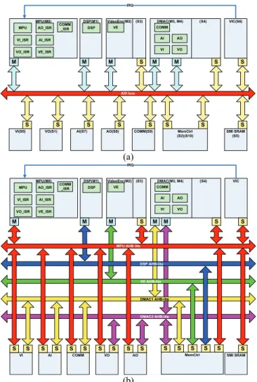
Fig. 4 illustrates the target platform from the memory controller’s point of view. The memory controller only connects with the AXI bus and the DRAM. Memory access requests are sent by the master devices connected to the AXI bus interconnect. The memory model is
AXI Bus Interconnect
CPU DSP Accelerator Video Capture Video Display Audio In Audio Out WLAN 3G Memory Controler Off-chip Data Memories Off-chip On-chip Off-chip Instruction Memories Inst. Memory Controler
based on Micron’s MT46V8M16 DDR SDRAM [21]. Note that only data memory is considered. Instruction memory and access are excluded because instruction memory can often achieve high bandwidth utilization due to predictable access behavior and pattern.
3.4.2.
Videophone Application
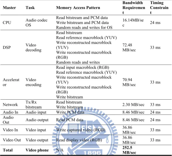
The target application adopted in our simulation platform is a video phone application. In this video phone application, the system must deliver both audio and video communication at the same time. The system supports 44.1 Khz stereo audio capture/output and audio compression/decompression. As to video, the system provides 4CIF sized video capture, compression/ decompression, and display with a frame rate of 30 FPS. Table 1 lists the task
Table 1 The task, access pattern, bandwidth, and completion time requirement of each master device Master Task Memory Access Pattern Bandwidth Requiremen
t
Timing Constrain t
CPU Audio codec OS Read bitstream and PCM data Write bitstream and PCM data Random reads and writes for OS
16.14MB/se
c 24 ms
DSP Video decoding
Read bitstream
Read reference macroblock (YUV) Write reconstructed macroblock (YUV)
Write reconstructed macroblock (RGB)
Random reads and writes
72.48
MB/sec 33 ms
Accelerat
or Video encoding
Read input macroblock (RGB) Read reference macroblock (YUV) Write reconstructed macroblock (YUV)
Write reconstructed macroblock (RGB)
Write bitstream
70.94
MB/sec 33 ms
Network Tx/Rx bitstream Read bitstream Write bitstream 2.30 MB/sec 33 ms Audio In Audio input Write PCM data 8.46 MB/sec 24 ms Audio
Out Audio output Read PCM data 8.46 MB/sec 24 ms
Video In Video input Write captured video (RGB) 36.86 MB/sec 33 ms Video Out Video output Read display video (RGB) 36.86 MB/sec 33 ms
description, minimal bandwidth requirement, and task completion time constraint of each master device in the video phone application. These system tasks are arranged in a pipelined fashion so that inter task dependency is minimized. The minimal memory bandwidth requirement for target performance is 252.5 MB/sec. If a memory controller can deliver more bandwidth, more data can be transferred within a second and better system speed can be achieved.
3.5.
Simulation Result
In this section, we evaluate the performance of different memory controllers on our simulation platform. The memory scheduling policies for comparison are No-Scheduling Nor-Bank-Interleaving (NSNBI), FIFS with bank-interleaving (FIFS), and LTSP. NSNBI represents the simplest memory controller without bank-interleaving support. FIFS represents the most common memory controllers with bank-interleaving support.
We investigated the impact of burst length, bus interface buffer size, and bus arbitration policy on bandwidth usage, memory power consumption, and memory energy efficiency.
3.5.1.
Evaluation Metrics
Table 2 lists the performance evaluation metrics and their physical meaning. The bandwidth usage (BU) evaluates how much data a memory controller can access within a second; it also implies shorter effective transaction latency from a system’s point of view. The memory power consumption evaluates scheduling policy impact on memory’s power consumption. However, scheduling policy that delivers higher bandwidth usage may also result in higher power consumption. Hence, we also use the memory energy efficiency to evaluate how much data a scheduling policy can deliver per unit energy. With memory energy consumption being the dominant part in a system, higher memory energy efficiency represents longer battery life and hence longer device operation time.
3.5.2.
Burst Length Impact
The effect of bus burst length 2, 4, 8, and 16 on DRAM performance is investigated. These bus burst length corresponds to memory burst length 4, 8, 16, and 32 on DDR memories because of the double data rate. The buffer size in both the masters and the memory controller are 8 entries.
A. Bandwidth Usage (BU)
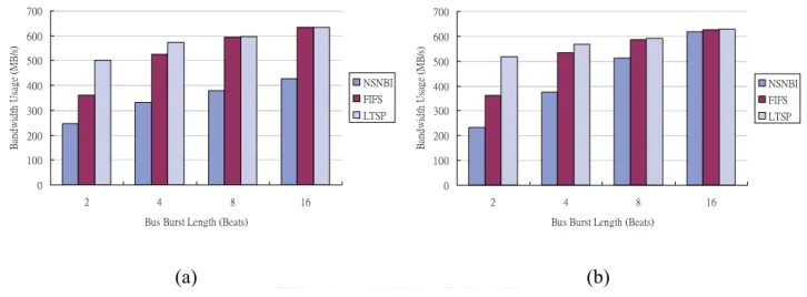
Fig. 5 shows the bandwidth usage of using LTSP scheduling policies is the highest among the compared scheduling policies. The bandwidth usage improvements compared with FIFS can reach up to 19.7% for burst length 2. However, for burst length 8 and 16, the bandwidth usage of using LTSP scheduling policy is slightly higher than that of FIFS. This is
Table 2 Performance evaluation metrics
Evaluation Metric Description Unit
Bandwidth Usage
The ratio between the total amount of data transferred and the total time taken to transfer the data.
MB/sec Memory Power Consumption The power consumed by DRAM estimated with Micron’s DRAM power calculator [16]. mW Memory Energy Efficiency The amount of data that can be accessed for a given amount of memory energy consumption. KB/mJ
0 100 200 300 400 500 600 700 2 4 8 16
Bus Burst Length (Beats)
B andw idt h U sa ge ( M B /s ) NSNBI FIFS LTSP 0 100 200 300 400 500 600 700 2 4 8 16
Bus Burst Length (Beats)
B and w idt h U sa ge ( M B /s ) NSNBI FIFS LTSP (a) (b)
because long burst length not only reduces the amount of row activation but also hides the long precharge and activation latency with the long data access time.
B. Memory Power Consumption
Fig. 6 shows that LTSP achieves the second lowest memory power consumption for burst length longer than 2. For burst length 2, however, LTSP has the highest memory power consumption. This is mainly due to the fact that the total time taken to transfer all the data when using LTSP policy is much shorter than others, hence decreasing the denominator in the power consumption formula. For burst length 4 and 8, at least 22 mW of power consumption can be reduced compared with burst length 2. However, the memory power consumptions of burst length 8 are almost the same as the power consumption of burst length 16. In contrast to LTSP’s second lowest memory power consumption, FIFS has the highest power consumption for burst length longer than 2.NSNBI can achieve the lowest memory power consumption in most cases because it performs fewer accesses within unit time than other policies. Note that the power consumptions are around 500mW and are at least an order larger than the power consumption of a memory controller itself. Hence, the power consumption overhead of the memory controller is insignificant compared with that of the memory module, which
dominates the power consumption of a multimedia platform.
0 100 200 300 400 500 600 2 4 8 16
Bus Burst Length (Beats)
M em or y P ow er ( m W ) NSNBI FIFS LTSP 0 100 200 300 400 500 600 2 4 8 16
Bus Burst Length (Beats)
Me m or y Po w er ( m W ) NSNBI FIFS LTSP (a) (b)
C. Memory Energy Efficiency
Fig. 7 shows that LTSP scheduling policy provides the highest energy efficiency in all cases. The efficiency improvements between LTSP and FIFS are 34.1%~4.0%. The improvement decreases as the burst length becomes longer due to the same reason why bandwidth usage saturates.
In summary, LTSP scheduling policy can provide both higher bandwidth utilization and memory energy efficiency, which is suitable for high performance and high energy efficiency applications. On the other hand, FIFS is an option to provide fair bandwidth usage when long burst length is available. However, FIFS has very high memory power consumption compared with other scheduling policies. Therefore FIFS is recommended for medium performance applications in which power consumption is less of an issue.
3.5.3.
Transaction Buffer Size Impact
This sub section presents the impact of using different transaction buffer size. The buffer size determines the number of transactions that can be scheduled. We investigate the scheduling policies used in previous section with buffer size 2, 4, 8, 12, and 16 entries. Each entry stores a transaction. The bus burst length is set to 4 for all cases.
0 200 400 600 800 1,000 1,200 1,400 2 4 8 16
Bus Burst Length (Beats)
M em o ry E n er gy Effi cie n cy ( K B /m J) NSNBI FIFS LTSP 0 200 400 600 800 1,000 1,200 1,400 2 4 8 16
Bus Burst Length (Beats)
M em or y E ne rgy E ff ic ie nc y (K B /m J) NSNBI FIFS LTSP (a) (b)
A. Bandwidth Usage (BU)
Fig. 8. illustrates the bandwidth utilization using different buffer size. For buffer size 2, the bandwidth utilizations of LTSP scheduling policy and FIFS are almost the same. For buffer size 4, the bandwidth utilization of LTSP is at least 6% higher than that of FIFS. In general, increasing the buffer size increases the bandwidth utilization because larger buffer size allows more transactions to be scheduled. Moreover, larger buffer size also reduces the possibility of the buffer being occupied by transactions accessing to only one particular bank. If all the transactions within the buffer try to access the same bank, only one transaction scheduler and command translator can be utilized. However, the improvement of bandwidth usage saturates as buffer size increases over 12. This is because all the transaction schedulers and command translators are already fully in use and hence scheduling capacity is reached. In addition, the utilization limit of the memory command bus also limits the maximum number of access commands that can be issued to DRAM.
B. Memory Power Consumption
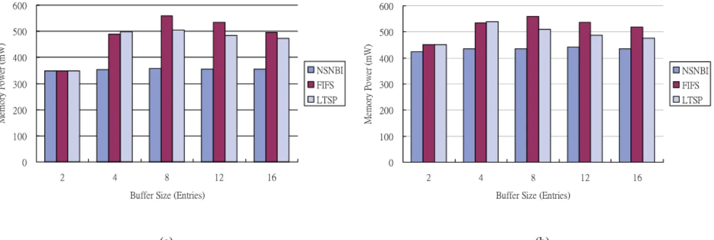
Fig. 9. illustrates the memory power consumption using different buffer size. For buffer size 2, the memory power consumptions of LTSP and FIFS are almost the same. For buffer size 4, the memory power consumption of LTSP is the highest. However, for buffer size larger than 4, the memory power consumption of FIFS becomes the highest. For buffer size
0 100 200 300 400 500 600 700 2 4 8 12 16
Buffer Size (Entries)
B andw idt h U sa ge ( M B /s ) NSNBI FIFS LTSP 0 100 200 300 400 500 600 700 2 4 8 12 16
Buffer Size (Entries)
B an dwi dt h Usa g e (M B /s) NSNBI FIFS LTSP (a) (b)
larger than 4, the power consumptions of LTSP and FIFS decrease gradually as the buffer size increases.
C. Memory Energy Efficiency
Fig. 10 reveals that the energy efficiency increases as buffer size increases for LTSP scheduling policy in general. Although there is still energy efficiency improvement between buffer size 12 and 16 using LTSP, the improvements is only 2.1% due to the saturation effect explained earlier. The energy efficiency improvement of FIFS has similar trend. However, the energy efficiency of FIFS is inferior to that of LTSP.
In summary, given that the system bus is adopting packet-based protocol, increasing the
0 100 200 300 400 500 600 2 4 8 12 16
Buffer Size (Entries)
M em o ry P o w er (m W ) NSNBI FIFS LTSP 0 100 200 300 400 500 600 2 4 8 12 16
Buffer Size (Entries)
M em ory P ow er (m W ) NSNBI FIFS LTSP (a) (b)
Fig. 9. Memory power consumption of different buffer size with (a)FP and (b)RR bus arbitration
0 200 400 600 800 1,000 1,200 1,400 2 4 8 12 16
Buffer Size (Entries)
M emor y E n er gy E ff ici en cy (K B /m J) NSNBI FIFS LTSP 0 200 400 600 800 1,000 1,200 1,400 2 4 8 12 16
Buffer Size (Entreis)
M emo ry E n er g y E ff ici ency ( K B /mJ ) NSNBI FIFS LTSP (a) (b) Fig. 10. Memory energy efficiency of different buffer size with (a)FP and (b)RR bus arbitration
efficiency for memory scheduling policies supporting bank-interleaving. However, the buffer size should not exceed 12 because of the saturation effect. Although with larger buffer size, the bandwidth usage of FIFS is only slightly lower than the bandwidth usage of LTSP. LTSP scheduling policy is still the better choice when memory energy efficiency is also an issue. From the simulation result, buffer size of 8 or 12 are suggested as the best trade-off on performance and buffer size.
3.5.4.
Bus Arbitration Policy Impact
This sub section discusses the impact of using fixed-priority (FP) or round-robin (RR) bus arbitration policies on performance.
A. Bandwidth Usage (BU)
The bus arbitration impact on bandwidth usage result in at most 1% difference for LTSP policy. FIFS is also less sensitive to bus arbitration policy when the buffer size is large enough; however, for buffer size 2, FIFS achieves higher bandwidth usage in RR than in FP. In contrast to LTSP being independent of bus arbitration policy, NSNBI has 25%~ 7% higher bandwidth usages in RR bus arbitration than in FP bus arbitration. This is because RR bus arbitration would result in higher access locality than FP bus arbitration would. If FP bus arbitration is used with longer burst, a row which was previously accessed by another device with higher bus arbitration priority would be re-opened. As a result, the access pattern would jump back and forth from one memory row to another from time to time. In contrast, RR bus arbitration has higher chances to group accesses from different devices together. Thus result in more row-hits and fewer row re-openings.
B. Memory Power Consumption
In both bus arbitration policies, the power consumptions of using LTSP are almost the same. This is due to the fact LTSP can reorder the transactions and is thus independent of which bus arbitration is being used. For NSNBI, the power consumption in FP bus arbitration