國 立 交 通 大 學
電子工程學系電子研究所
博 士 論 文
無線近距離資料傳輸
基頻收發器設計技術之研究
Baseband Design Techniques for
Wireless Proximity Data Transmission
研究生 : 游瑞元
指導教授 : 李鎮宜博士
無線近距離資料傳輸
基頻收發器設計技術之研究
Baseband Design Techniques for
Wireless Proximity Data Transmission
研 究 生: 游瑞元 Student: Jui-Yuan Yu 指導教授: 李鎮宜博士 Advisor: Dr. Chen-Yi Lee
國立交通大學
電子工程學系電子研究所
博士論文
A Dissertation
Submitted to Department of Electronics Engineering & Institute Electronics College of Electrical and Computer Engineering
National Chiao Tung University in Partial Fulfillment of Requirements for the Degree of Doctor of Philosophy
in
Electronics Engineering July 2008
Hsinchu, Taiwan, Republic of China
無線近距離資料傳輸
基頻收發器設計技術之研究
研 究 生: 游瑞元 指導教授: 李鎮宜教授 國立交通大學電子工程學系電子研究所摘要
無線應用中的近距離資料通訊系統為本論文專注的主軸。在這樣的系統中,功率和 效能是最主要需要克服的問題,而本論文著重在使用全數位的設計方案來降低功率與增 進系統效能。而這些方案的驗證平台則是使用無線正交展頻調變為基礎的基頻處理器。 近距離資料通訊的相關問題,則是在兩個系統中來探討與評估。一為IEEE 802.15.3a MB-OFDM 超寬頻系統;另一則為自有定義之系統,命名為 uPHI/WiBoC。這兩者系統 分別歸類於無線個人網路(WPAN)以及無線近身網路(WBAN)當中。這兩個系統的共通 特性為以封包為基礎之短距離通訊系統。在使用的超寬頻系統中,其傳輸數率為 480Mb/s,在這樣的高速傳輸速率之下,系統效能顯得相當容易受到非理想效應干擾, 而傳輸與接收功率也分別被定義在180mW 與 323mW 以下。在自有定義之 uPHI/WiBoC 系統下,則是專注在一毫瓦以下(sub-mW)的功率設計方案,同時其傳輸速率則屬於低速 的系統 (<10Mb/s)。綜合上述情境下,本文在基頻處理器中提出幾樣以數位設計方案, 來達到低功率與高效能的目的,而這樣的設計理念可同時應用在低速與高速無線短距離 通訊系統之中。 第一個方案為全數位式鏡相消除技術,用來解決 RF 與基頻訊號在轉換過程中所產 生的實虛兩軸不批配的問題,這個現象消減基頻處理器在解調變訊號的效能。在這個方 案之中,定義了一個誤差函數,可應用在窄頻與寬頻的條件之下,此誤差函數使得系統可使用可適性的技術來達到系統效能改進。此方案可以校正 2dB 的增益誤差及 20∘的 相位誤差。同時最大可以改善2.5dB 的訊躁比。 在動態取樣時序控制的方案當中,可將訊號取樣頻率從 Nyquist 或更高的頻率調降 至符號頻率。此數位智慧型控制方案大幅降低基頻的功率消耗,同時使得訊號可在最佳 取樣點取樣。使用此智慧型控制方案,最大可以增進1.7dB 的訊躁比,同時可以有效降 低40%功率消耗。 在遲滯電路的設計方案之中,本概念使用於全數位控制震盪器中,此震盪器可應用 於全數位鎖相迴路與全數位延遲迴路之中。這兩個迴路的應用情境,通常為持續作動的 電路,因此通常會連續消耗動態與靜態功率。而這個遲滯電路與一般的標準函式庫元件 相較起來,在訊號延遲產生效果上,可降低72.12~99.26%的功率消耗。而在整體全數位 控制震盪器效能上,則可以降低98%的功率以及 95%的面積。 在硬體實現部分,則是藉由超寬頻與uPHI/WiBoC 的基頻處理器來驗證相關方案的 概念。超寬頻基頻處理器整合了全數位鏡相消除技術與動態取樣時序控制技術,降低了 40%的功率消耗。而在 uPHI/WiBoC 基頻處理器,則是應用了電壓域以及功率域的分割 方案,來達到以電路層級的功率控制與能量節省,這使得此基頻處理器能夠操作在最低 0.5V 的電壓,達到 10μW 以下的功率消耗。
Baseband Design Techniques for
Wireless Proximity Data Transmission
Student: Jui-Yuan Yu Advisor: Chen-Yi Lee Department of Electronics Engineering and Institute of Electronics,
National Chiao-Tung University
Abstract
Proximity data communications in wireless applications are targeted in this work. The proposals are studied to overcome power and performance issues in this communications scenario. The power reductions and performance improvements are all achieved by digital approaches evaluated in a wireless OFDM-based baseband processor.
The proximity data communications is explored and evaluated in the IEEE 802.15.3a MB-OFDM UWB and an in-house designed system (uPHI/WiBoC) that corresponds to the wireless personal area network (WPAN) and the wireless body area network (WBAN), respectively. Both of them are packet-based short range wireless communications schemes. The MB-OFDM UWB is designed for high speed 480Mb/s transmissions so that it is performance sensitive in such high rate communication with power budget no more than 180mW and 323mW in transmission and receiving, respectively. The uPHI/WiBoC system is designed with low rate communications (<10Mb/s) in the sub-mW power constraint. Accordingly, this work proposes several digital-based schemes in the baseband for power reductions and performance improvements to meet both the low-rate to high speed short range wireless communications systems.
The first proposal is an all-digital I/Q-mismatch cancellation (ADIQMC) proposed to solve I/Q mismatch during RF conversions that degrades baseband decoding performance. This work defines the error function in both narrow and wide band channel so that the error
cancellation can be achieved adaptively. The gain- and phase-error tolerances are 2dB and 20∘, respectively, with maximum 2.5dB SNR reduction.
The dynamic sample-timing control (DSTC) reduces the sampling rate in an ADC circuit from Nyquist rate or higher rate to the symbol rate. This digital smart control scheme largely reduces the baseband power consumption and enables the best-position signal sampling. This DSTC scheme enables a possible maximum 1.7dB SNR improvement with 40% power reduction.
The hysteresis delay cell (HDC) is designed and applied to the utilization in a digitally controlled oscillator (DCO) that may be used in an all-digital phase locked loop (ADPLL) or an all-digital delay locked loop (ADDLL). The DCO circuits in an ADPLL or an ADDLL are an always-active circuits that continuously consume dynamic and static power even in the chip inactive duration. The HDC, depending on the topologies, provides a 72.12~99.26% power reduction compared to a cell-based delay cell. The overall DCO dynamic power and area with the HDC designs are reduced by 98% and 95%, respectively, compared to a cell-based DCO design.
The baseband processors are implemented in both of the MB-OFDM UWB and uPHI/WiBoC systems. The UWB baseband processor integrates the ADIC and DSTC circuits, providing a 40% power reduction evaluated with a whole physical layer circuits. The uPHI/WiBoC applies the voltage-domain and power-domain partitions for circuit-level power control and energy saving. This enables the WBAN baseband processor operated in minimum supply voltage 0.5V with sub-10μW power consumption.
誌謝
在Si2 實驗室的幾年中,是讓我在交大成長最多的一段時間。從大三專題開始學習 做研究、第一次出國參加國際會議學習面對世界的舞台、與學弟妹們組織研究團隊、並 且學習讓研究成果對外呈現、以及一切無法言語的體會,都要感謝一路引導我的指導教 授李鎮宜博士,在這過程提供了非常完善的學習環境,並且讓我有不斷嘗試錯誤的空 間,並且在許多沮喪的時刻提供精神上的支持,同時藉由研究過程,更讓我從老師身上 學習到對人處事及眼光的培養。另外,也要感謝口試委員黃威教授、任建葳教授、魏慶 隆教授、陳紹基教授、周世傑教授、黃家齊教授、蘇朝琴教授、及王晉良教授們能夠在 百忙之中來替學生口試與指導,使得本篇論文能夠更加完整。同時更要特別感謝鍾菁哲 教授在我研究論文的準備過程、投稿撰寫、以及口試準備的過程中,提供了許多寶貴的 意見,也可以說是我在生活中的良師益友。 此外,在Si2 實驗室裡面讓我最珍惜的也是與所有成員們的互相學習。在這邊要感 謝許騰尹教授替我引導並建構一個良好的學習環境,張錫嘉教授能夠時時刻刻非常貼心 的提供寶貴的建議,劉軒宇博士在研究與論文給了許多協助,做為我一個研究上最好的 榜樣,陳元學長非常有耐心的給予各種角度的建議和討論。我也要特別感謝與我一同並 肩作戰的學弟妹們:婉君、美慧、建螢、燦文、上賓、俊廷、偉豪、曉涵、書餘、士恒、 曼嘉,因為有你們,使得我在面對瓶頸時更有力量。在這段研究期間,也要同時感謝聯華電子提供University Shuttle Program 讓我們有
機會可以在先進製程上面驗證我們的電路行為,同時也要感謝聯發科這段時間在研究助 學金上的提供,得以使得研究過程中更無後顧之憂。 在這幾年,我要感謝一直陪伴著我的女友敏筠及敏筠家人,能夠無時無刻給予鼓勵 與支持,分享我的喜怒哀樂。最後,我要由衷的感謝爸爸及媽媽,因為有你們從小的培 養,使得我有機會進入研究的殿堂,也因為有你們在這幾年時時刻刻的引導,使得我不 斷的成長更體會到您的偉大,在這邊以此論文獻給您們,做為我們全家共同分享的成果。
CONTENTS
CONTENTS
PAGE
Chapter 1: Motivations ... 1
1-1 All-digital I/Q-mismatch cancellation (ADIQMC) for RF front-end performance improvement ... 6
1-2 Dynamic sampling-timing control (DSTC) for ADC power reduction ... 7
1-3 Hysteresis delay cell (HDC) for clock generator power reduction ... 7
1-4 Dynamic coarse-grain power control (DCGPC) for power reduction ... 8
1-5 Embedded silicon-crystal generation (ESCG) for cost and power reduction ... 9
Chapter 2: Introduction... 10
2-1 Multi-Band OFDM Ultra Wideband in WPAN ... 13
2-2 In-House Protocols (uPHI & WiBoC) in WBAN ... 17
2-2-1 Application Scenarios ... 17
2-2-2 WBAN System Design Constraints ... 22
2-2-3 uPHI Specifications... 26
2-2-4 WiBoC Specifications ... 30
Chapter 3: I/Q-Mismatch Calibration... 35
3-1 Background and Overview ... 35
3-2 I/Q-Mismatch Modeling ... 39
3-3 I/Q-Mismatch Compensation... 43
3-3-1 Time-domain compensation ... 45
3-3-2 Frequency-domain compensation ... 46
3-4 IQM Parameter Estimations... 46
3-4-1 Narrow-band adaptive estimation ... 46
3-4-2 Wide-band-based estimation ... 53
3-5 Simulation Results ... 58
3-5-1 Narrow-band adaptive scheme ... 58
3-5-2 Wide-band scheme ... 67
CONTENTS
Chapter 4: Dynamic Sampling-Timing Control... 75
4-1 Background and Overview ... 75
4-2 System Introduction... 79
4-3 Dynamic Sample-Timing Control ... 81
4-3-1 Sinc Filter ... 82
4-3-2 Raised-Cosine Filter... 83
4-3-3 Butterworth Filter... 84
4-4 Simulation Results ... 93
4-5 Summary ... 115
Chapter 5: All-Digital Hysteresis-Based Clock Generator ... 117
5-1 Background and Overview ... 117
5-2 The P2-DCO Architecture ... 120
5-3 Coarse Tuning Delay Cells... 121
5-3-1 Large-Scale Hysteresis Delay Cell (LHDC)... 121
5-3-2 Very Large-Scale Hysteresis Delay Cell (VLHDC)... 122
5-4 Fine Tuning Delay Cells... 127
5-4-1 Medium/Small-Scale Hysteresis Delay Cell... 128
5-4-2 MOS Gate Capacitance (MGC) ... 133
5-5 Simulation Results and Comparisons ... 133
5-6 Summary ... 138
Chapter 6: Case Study ... 139
6-1 Introduction... 139
6-2 Case 1: MB-OFDM UWB baseband processor... 140
6-2-1 Baseband Modem Designs... 140
6-2-2 Phase-Tunable Clock Generator ... 147
6-2-4 Simulation and Experimental Results ... 149
6-3 Case 2: WBAN WiBoC baseband processor... 159
6-3-1 Low Power Design Flow... 159
CONTENTS
Chapter 7: Conclusion and Future Work... 198
7-1 Conclusion ... 198
7-2 Future Work ... 199
Appendix I: Voltage-Power Domain Designs... 200
Appendix II: Power Gating Cell Exploration... 204
A2-1 Introduction ... 204
A2-2 Power Gating Cell Fundamental Exploration... 206
A2-2-1 Header vs. Footer ... 206
A2-2-2 NMOS-Header vs. PMOS-Header ... 207
A2-3 Power Gating Cell Fundamental Exploration... 212
A2-3-1 Leakage Characteristics... 212
A2-3-2 Performance Evaluations... 214
LIST OF FIGURES
LIST OF FIGURES
PAGE
Fig. 1-1. The two trends in semiconductor developments ... 1
Fig. 1-2. The more-Moore and more-than-Moore spectrum... 3
Fig. 1-3. The contribution matrix ... 5
Fig. 1-4. The evaluation vehicle... 5
Fig. 2-1. The target short range platforms for evaluations ... 12
Fig. 2-2. The band group plans in the UWB spectrum ... 15
Fig. 2-3. The example of band transitions in a band group ... 15
Fig. 2-4. Packet format of MB-OFDM UWB system... 16
Fig. 2-5. Network in wireless body area network applications... 18
Fig. 2-6. Multiple sensors in coexistence operation scenarios... 20
Fig. 2-7. Applications on wearable devices ... 21
Fig. 2-8. Implanted devices in WBAN applications ... 22
Fig. 2-9. Design features in wearable and implant WBAN links ... 24
Fig. 2-10. Spectrum distribution and reliability for WMTS, UWB, and ISM bands ... 26
Fig. 2-11. Brief uPHI block diagram in a WSN ... 27
Fig. 3-1. The role of the digitally RF front-end calibration in the power and data proximity scheme ... 36
Fig. 3-2. OFDM receiver with frequency-selective IQM ... 40
Fig. 3-3. IQM distorted signals with (a) constant gain and phase errors (signal and image gains) (b) frequency-selective gain and phase errors (signal and image gains). ... 42
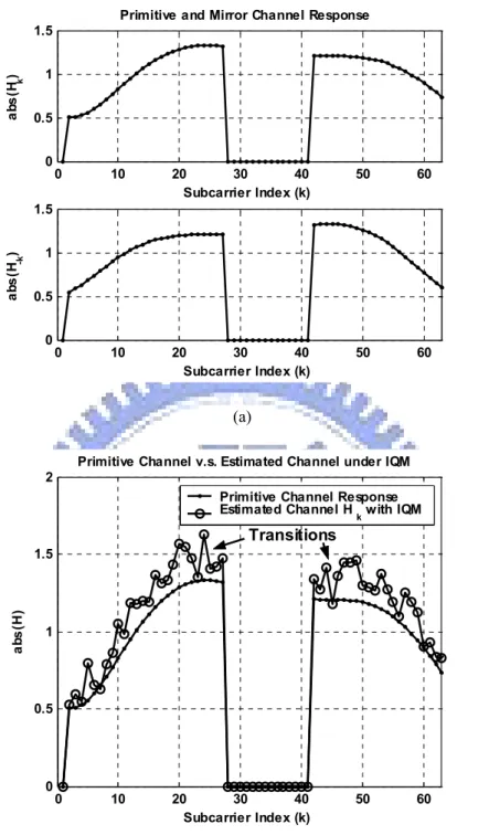
Fig. 3-4. Channel response with IQM effect (a) primitive channel response and the mirror response (b) estimated channel response under gain error 1 dB and phase 10 degree... 49
Fig. 3-5. Summary of the overall adaptation loop. ... 51
Fig. 3-6. Summary of the overall adaptation loop. ... 52
Fig. 3-7. The packet format for IQM estimation... 54
Fig. 3-8. Summary of the overall estimation and compensation behavior. ... 57
Fig. 3-9. Summary of the overall estimation and compensation behavior. ... 57
Fig. 3-10. System performance without IQM correction under Rayleigh fading channel. The reached SNR at PER 0.1 with different gain and phase error values (a) the 3-D view (b) the corresponding projection in 2-D view. ... 59
Fig. 3-11. Δ convergence with G.E. 1dB and P.E. 10 degree in Rayleigh fading channel β @ SNR 25dB. ... 60
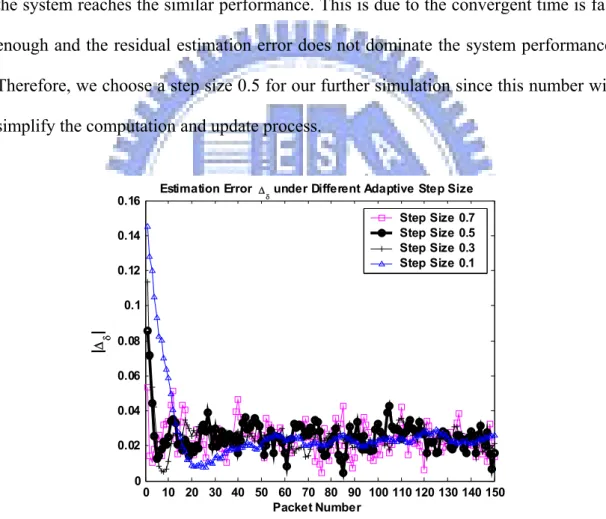
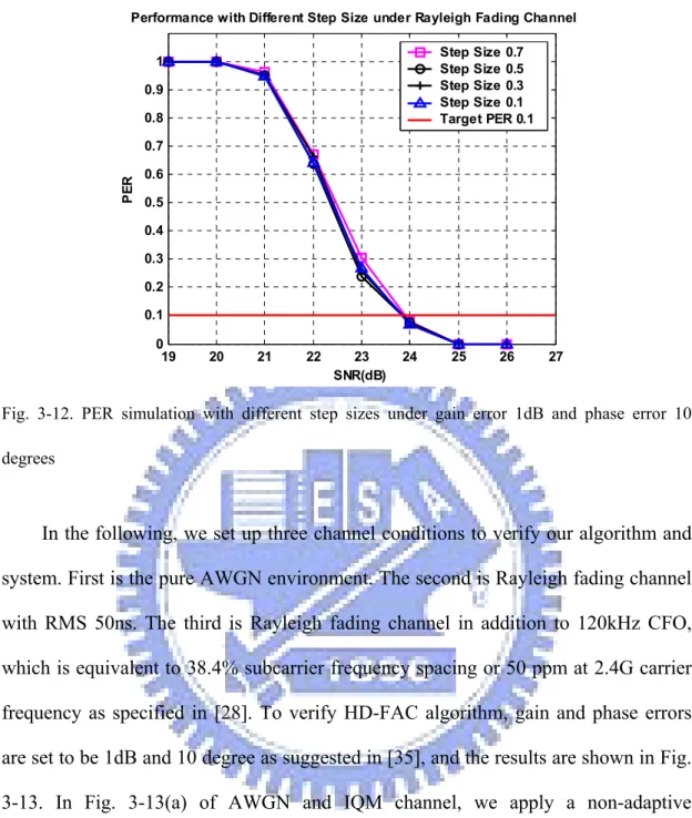
Fig. 3-12. PER simulation with different step sizes under gain error 1dB and phase error 10 degrees ... 61
Fig. 3-13. IQM compensation performance with GE 1 dB and PE 10 degree under (a) AWGN channel (b) Rayleigh fading channel (c) Rayleigh fading and CFO channel. .. 63
LIST OF FIGURES
Fig. 3-14. Estimated channel resopnse with the proposed HD-FAC under gain/phase errors1dB and 10 deg., and Rayleigh fading channel RMS 50ns @ SNR 30dB... 65
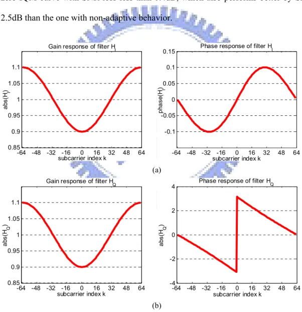
Fig. 3-15. Constellation with the proposed HD-FAC under gain/phase errors 1dB and 10 degrees and Rayleigh fading channel RMS 50ns @ SNR 30dB (a)Initial State (b)Stable State. 66 Fig. 3-16. The frequency-selective IQM modeling with transfer function of (a) filter HI (b) filter HQ... 69
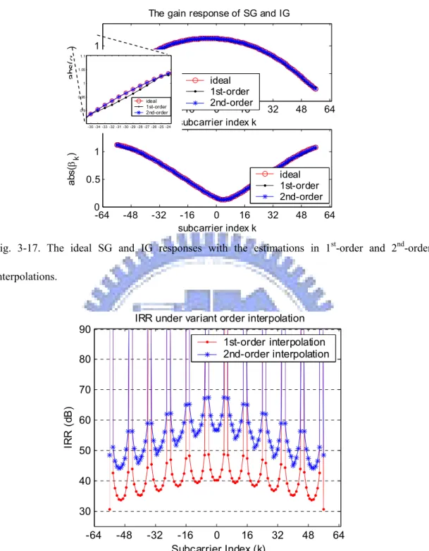
Fig. 3-17. The ideal SG and IG responses with the estimations in 1st -order and 2nd -order interpolations. ... 70
Fig. 3-18. The image rejection ratio (IRR) after compensation in a frequency selective IQM condition. ... 70
Fig. 3-19. The signal constellation under the frequency-selective IQM in 1dB gain error and 10o phase error (a) without and (b) with calibration. ... 71
Fig. 3-20. The signal constellation under the frequency-selective IQM in 1dB gain error and 10o phase error (a) without and (b) with calibration in a SNR 20dB AWGN channel. . 72
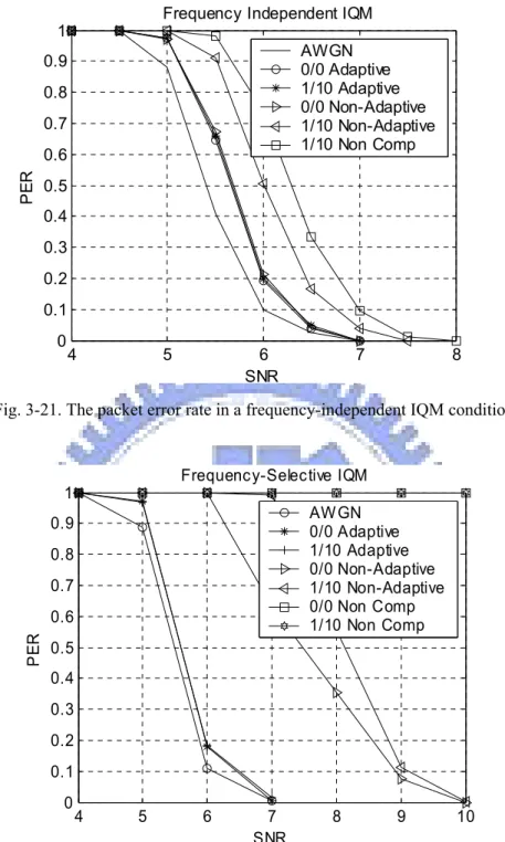
Fig. 3-21. The packet error rate in a frequency-independent IQM condition... 73
Fig. 3-22. The packet error rate in a frequency-selective IQM condition. ... 73
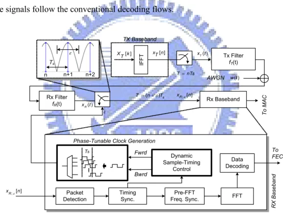
Fig. 4-1. The role of the dynamic sample-timing control in the power and data proximity scheme ... 76
Fig. 4-2. The power and operating frequency for ADC circuits... 78
Fig. 4-3. Block diagram of the proposed baseband receiver with the aid of the proposed dynamic sample-timing control (DSTC) and phase-tunable clock generation (PTCG). .. 81
Fig. 4-4. Sinc function impulse response ... 83
Fig. 4-5. Raised-cosine filter function impulse response with β= {0.2, 0.5, 0.8} ... 84
Fig. 4-6. Butterworth function impulse response... 85
Fig. 4-7. The signal-to-interference-ratio (SIR) for a sinc function impulse resopnse... 87
Fig. 4-8. The signal-to-interference-ratio (SIR) for a raised-cosine filter impulse response ... 87
Fig. 4-9. The signal-to-interference-ratio (SIR) for a 5th -order Butterworth filter impulse response ... 88
Fig. 4-10. Characteristic function of a sinc function... 92
Fig. 4-11. Characteristic function of a raised cosine filter... 92
Fig. 4-12. Characteristic function of a 5th -order Butterworth filter... 93
Fig. 4-13. Packet frame and waveform property for the DSTC operation ... 94
Fig. 4-14. Packet frame used for the DSTC computation... 95
Fig. 4-15. The operation flow for the DSTC computation ... 96
Fig. 4-16. The flow and methodology for DSTC simulations ... 102
Fig. 4-17. System performances on a corresponding sampling instance and the determined sampling-timing probability with DSTC algorithm in the sinc function condition... 103
LIST OF FIGURES
Fig. 4-18. System performances on a corresponding sampling instance and the determinedsampling-timing probability with DSTC algorithm in the RC function condition... 105
Fig. 4-19. System performances on a corresponding sampling instance and the determined sampling-timing probability with DSTC algorithm in the RC function condition... 105
Fig. 4-20. System performances on a corresponding sampling instance and the determined sampling-timing probability with DSTC algorithm in the RC function condition... 106
Fig. 4-21. System performances on a corresponding sampling instance and the determined sampling-timing probability with DSTC algorithm in the Butterworth function condition ... 106
Fig. 4-22. The decoded QPSK symbol constellation with the best sampling instance in β=0.5 raised-cosine filter condition... 107
Fig. 4-23. The decoded QPSK symbol constellation with the worst sampling instance in β=0.5 raised-cosine filter condition... 107
Fig. 4-24. System performance with 2-time interpolation scheme ... 109
Fig. 4-25. Resulted system performance in variant PTCG phase number... 112
Fig. 4-26. CF function to the corresponding sampling timing error... 115
Fig. 5-1. The role of the dynamic sample-timing control in the power and data proximity scheme ... 118
Fig. 5-2. The power-of-two delay stage DCO block diagrams... 121
Fig. 5-3. The proposed delay cells (a) large-scale hysteresis delay cell (LHDC); (b) very-large-scale hysteresis delay cell (VLHDC)... 124
Fig. 5-4. The example case (a) LHDC0 schematic (b) LHDC0 generated waveforms... 125
Fig. 5-5. The example case (a) VLHDC0 schematic (b) VLHDC0 generated waveforms... 127
Fig. 5-6. The proposed delay cells (a) medium-scale hysteresis delay cell (MHDC); (b) small-scale hysteresis delay cell (SHDC)... 129
Fig. 5-7. The example case (a) MHDC0 schematic (b) MHDC0 generated waveforms ... 131
Fig. 5-8. The example case (a) MHDC0 schematic (b) MHDC0 generated waveforms ... 132
Fig. 6-1. The role of the chip implementation in the power and data proximity scheme (a) design hierarchy; (b) design building blocks... 140
Fig. 6-2. Block diagrams in the MB-OFDM WUB transceiver (a) transmitter (b) receiver... 141
Fig. 6-3. Developments and verifications between system behavior and hardware implementation ... 142
Fig. 6-4. The block diagrams of the proposed MB-OFDM UWB baseband processor ... 144
Fig. 6-5. The proposed wideband adaptive ADIC I/Q mismatch calibration scheme ... 145
Fig. 6-6. DSTC block diagram and operation architecture ... 147
Fig. 6-7. The proposed phase-tunable clock generator (PTCG) ... 148
LIST OF FIGURES
Fig. 6-9. Generated PTCG waveforms: (a) the simulated waveforms and (b) the measuredwaveforms... 151
Fig. 6-10. The illustrations of a glitch generation in improper forward and backward controlling... 151
Fig. 6-11. The power reduction and overhead with DSTC... 152
Fig. 6-12. Pie chart of RX signal power ... 155
Fig. 6-13. Pie chart of RX signal power ... 156
Fig. 6-14. Micro-photo of the test chip in 0.13μm standard CMOS technology ... 157
Fig. 6-15. The decoded constellation example... 158
Fig. 6-16. Chip testing platform ... 158
Fig. 6-17. Circuit synthesis in the low-power design flow ... 160
Fig. 6-18. Circuit implementation in the low-power design flow... 163
Fig. 6-19. The example circuit of a level shifter... 164
Fig. 6-20. The example circuit of an isolation cell ... 165
Fig. 6-21. The example circuit of a power gating cell... 165
Fig. 6-22. The block diagram of the MT-CDMA baseband transmitter... 167
Fig. 6-23. An illustration on the sleep and active phases in a WSN-CPN transmission link... 168
Fig. 6-24. The leakage saving efficiency to the SRAM word length size... 168
Fig. 6-25. Abstract view of the circuit block partitions in terms of power domains... 170
Fig. 6-26. The block diagram of the MT-CDMA demodulator in the CPN circuit ... 171
Fig. 6-27. The DSTC algorithm applied to the MT-CDMA demodulator in the CPN side... 173
Fig. 6-28. The adaptive ADIC I/Q mismatch calibration applied to the MT-CDMA demodulator in the CPN side ... 173
Fig. 6-29. The current profile of the MT-CDMA modulator in the active and sleep phases... 174
Fig. 6-30. The virtual VDD profile from sleep phase to active phase... 174
Fig. 6-31. The pie chart of the area percentage of a MT-CDMA demodulator in a CPN circuit . 175 Fig. 6-32. The pie chart of the power percentage of a MT-CDMA demodulator in a CPN circuit ... 176
Fig. 6-33. The pie chart of the power percentage of a MT-CDMA demodulator in a CPN circuit in terms of dynamic power and leakage power ... 177
Fig. 6-34. The bar chart of the dynamic and leakage power in each operation module ... 177
Fig. 6-35. The power reduction in the (a) WSN and (b) CPN... 178
Fig. 6-36. Micro-photo of the WSN and CPN chip set in 90nm standard CMOS technology ... 179
Fig. 6-37. Testing environment for the MT-CDMA modem test chips... 180
Fig. 6-38. The dual-mode baseband transceiver with (a) abstract view of functional blocks and (b) behavior time-line ... 181
Fig. 6-39. The transceiver with power domain planning (a) wireless sensor node (WSN); (b) central processing node (CPN) ... 182
LIST OF FIGURES
Fig. 6-40. The power management cell (PMC)... 183
Fig. 6-41. The power management control sequence ... 184
Fig. 6-42. The baseband transceiver with RSD frequency pre-calibration... 187
Fig. 6-43. The proposed PFTCG architecture... 190
Fig. 6-44. The control loop of the PFTCG circuits... 190
Fig. 6-45. The DCO block diagram ... 191
Fig. 6-46. The fine-tuning delay stage ... 191
Fig. 6-47. The generated waveforms from the PFTCG (a) operation overview (b) multi-phase waveforms... 193
Fig. 6-48. Clock phases from the PFTCG circuits... 195
Fig. 6-49. Current profile between the sleep and active phases ... 196
Fig. 6-50. Micro-photo of the dual mode test chip in 90nm standard CMOS technology... 196
Fig. A1-1. Initial module and power domain partitions... 200
Fig. A1-2. The floor planning in the scope of voltage and power domain partitions ... 201
Fig. A1-3. The results of power planning ... 201
Fig. A1-4. Standard cell placement in addition to the level shifter insertions ... 202
Fig. A1-5. Standard cell placement in addition to the isolation cell insertions... 203
Fig. A1-6. Final chip view with bonding pads attached ... 203
Fig. A2-2. Power gating cell operation mechanism (a) PMOSH (b) NMOSH ... 209
Fig. A2-3. NMOS:VD(0.5V)+VG(0.9V) and PMOS:VS(0.5V)+VG(0V) (a) driving current (b) transconductance... 211
Fig. A2-4. The proposed charge-pumped NHCMOS (CP-NHCMOS). ... 217
Fig. A2-5. The control signals and the corresponding timing order... 217
Fig. A2-6. Test circuit for performance evaluations ... 217
Fig. A2-7. Delay penalty vs. power switch size... 218
Fig. A2-8. Restored time of virtual VDD (VDDV) ... 219
LIST OF TABLES
LIST OF TABLES
PAGE
Table 2-1. Data rate parameters of MB-OFDM-based UWB system... 14
Table 2-2. System perameter summary... 16
Table 2-3. Power budget of PHY layer of IEEE 802.15.3a system... 17
Table 2-4. Power budget of PHY layer of IEEE 802.15.3a system... 25
Table 2-5. uPHI system parameter summary... 29
Table 2-6. WiBoC system parameter summary ... 32
Table 2-7. uPHI and WiBoC system parameter summary... 33
Table 3-1. SNR LOSS UNDER DIFFERENT CHANNEL CONDITIONS... 64
Table 3-2. COMPUTATION REQUIREMENT... 67
Table 4-1. System performance summary with DSTC and 2x interpolation... 110
Table 5-1. Delay cell summaries and comparisons... 137
Table 5-2. DCO Summarizes and Comparisons ... 137
Table 5-3. Comparisons to The State of The Art... 138
Table 6-1. Summary of power reduction ... 153
Table 6-2. A list of 10-bit ADC power ... 154
Table 6-3. A list of 8-bit ADC power ... 154
Table 6-4. ADCs reported in academic papers ... 155
Table 6-5. The implementation and function summary... 157
Table 6-6. The area of the MT-CDMA CPN circuit... 175
Table 6-7. The Power of the MT-CDMA CPN circuit ... 176
Table 6-8. The MT-CDMA transceiver chipset summary ... 178
Table 6-9. Chip core power in the dual-mode WSN and CPN chipset ... 195
Table 6-10. The dual-mode transceiver Chip Summary ... 197
Table 7-1. The Summary of This Work... 198
Table A2-1. Minimum leakage search with combinations of VG and VB ... 216
Table A2-2. leakage variations with unchanged [VG,VB] but changed PVT... 216
Table A2-3. Leakage current summary in different design schemes... 218
Table A2-4. Required energy overhead from sleep state to active state ... 218
Chapter 1:
Motivations
More Moore and more than Moore are currently opposite but both critical trends in semiconductor developments. These dual trends correspond to the Moore’s Law and system integration law as illustrated in Fig. 1-1 [1]. More Moore is achieved by integrating more and more transistors into a specific core area, providing a condensed chip design circuitry. On the other hand, the trend of the more than Moore presents heterogeneous integrations with existing technologies, such as semiconductor, micro-electro-mechanical systems (MEMS), scavenging energy source, etc.
1970 101 102 1010 109 108 107 106 105 104 103 2004 2020 2010 2000 1990 1980 101 102 1010 109 108 107 106 105 104 103 T ran sis to rs/cm 2 Comp one nts /c m 2
Moore Law for ICs
System Integration Law 1971 Multichip module System-in-package System-on-package 50
More Moore trend is pursued in increased processing speed and chip computing power. Those applications are required with shorter processing time and more function services. Wireless systems toward this tendency may be found in IEEE 802.11b, 802.11a/g, UWB, and next generation Giga-bit/sec UWB that serve higher data rate with increased processing speed and signal bandwidth as the technology process progresses. The high-data-rate demands require higher computation complexity and hardware cost to achieve large media transmissions. This implies that more and more transistors are integrated in a wireless chip, especially a digital baseband processor. As a result, power consumption becomes the vital problem, especially integrated in a portable device.
The more-than-Moore trend faces design challenges in integrating several components into a tiny stack, including reductions of device area and eliminations of external components. These can be particularly found in wireless sensor-oriented devices applied in the systems such as wireless body area networks (WBAN) or wireless sensor networks. One key point in designing more-than-Moore based heterogeneous devices is the reduction of circuit power. The target power in a device is suggested below micro-Watt (μW). If this μW-device is achieved, lots of energy-limited sources by scavenging-based approaches like motions, temperatures, or solar power can be attached with an extreme tiny size or even integrated inside. Otherwise, it is necessary to replace those scavenging sources with high-capacity battery for a normal device operation if large power is drawn. In other words, a tiny device is achieved only when little power is consumed in the circuits. However, it is not easy to reduce device power without eliminations of external components. Any passive or active external components result in large power waste compared with any integrated circuits because signals have to go through many unnecessary paths for the
reasons of level translations, signal protections, etc. This largely reduces energy efficiency and increases difficulty in the device-size shrinking. Accordingly, low power is required for heterogeneous devices to achieve tiny area, and eliminations of external components are one of the ways to achieve the low-power purpose.
A general spectrum of the more-Moore and more-than-Moore trends is shown in Fig. 1-2. This spectrum summarizes the key categories towards more-Moore and more-than-Moore sides. The more-Moore side may have baseline CMOS and memory designs. For the possible designs with variant material substrates, the more-than-Moore side may include the radio-frequency (RF) circuits, high-voltage (HV) power designs, passive components, sensor devices, and further bio-oriented interfaces.
More Moore More Than Moore
Computation
Interaction with users and
environments Baseline CMOS Memory RF HV Power Passives Sensors, Actuators Bio, Fluidics Dissertation Targets
In the progress of this two-trend spectrum of semiconductor industry, the power, performance, and cost always play crucial role that may possible dominate the market development and applications. As each item in this spectrum proceeds to advanced or higher integration, those indicator matrices (power, performance, and cost) becomes more and more difficult to solve. Accordingly, this dissertation focuses on the problem solving in the bottleneck of (1) baseline CMOS (2) RF circuits (3) passive components. The evaluation cases will be the wireless communications systems on the OFDM-based modulation scheme.
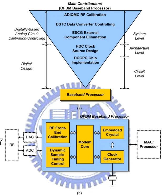
The improvements of baseline CMOS, RF circuits, and passive components may target on power saving, performance improvement, and area shrinking for highly integration. Those can be explored by the point of view in the system level, architecture level, and circuit level as illustrated in Fig. 1-3. Moreover, the approaches may be also considered as digitally-based analog circuit calibration/controlling or all digital designs. In the system level approach, the all-digital I/Q-mismatch cancellation RF calibration is applied to improve RF circuit and overall system performance in digital signal process. Furthermore, a dynamic sampling-timing control (DSTC) approach controls the sampling timing of data converters, providing better system performance and reduced power consumption. Then an embedded silicon-crystal generator (ESCG) is designed for the passive component elimination of external crystal. Then, a hysteresis delay cell (HDC) clock source design corresponds to the baseline CMOS design that targets mainly on an-order power reduction in the clock generation design. In the circuit-level design considerations, the distributed coarse-grain power control (DCGPC) is utilized for power reduction in the baseline CMOS circuit designs.
In the evaluation platforms, OFDM-based wireless communications systems, those design innovations are achieved and demonstrated in a baseband circuit, as shown in Fig. 1-4. Those building blocks have the design philosophy that improves the baseline CMOS, RF circuits, and the passive component eliminations.
Digitally-Based Analog Circuit Calibration/Controlling Digital Design ADIQMC RF Calibration DSTC Data Converter Controlling
HDC Clock Source Design DCGPC Chip Implementation ESCG External Component Elimination Main Contributions
(OFDM Baseband Processor)
System Level Architecture Level Circuit Level Baseband Processor
Fig. 1-3. The contribution matrix
RF Front-End Calibration Dynamic Sample-Timing Control Modem Core
OFDM Baseband Processor
MAC/ Processor RF ADC DAC ADC ADC Clock Generator Embedded Crystal
The main idea to achieve the proximity data and power transmission is to modify some analog-circuit behaviors of those components, like RF circuits, analog-to-digital converters (ADC), and external crystal, into a digital-based design that can largely reduce the design efforts of those collaborative devices. Moreover, the digital design itself also adopts circuit-topology techniques to further reduce power consumption. In other words, the data and power issues of a wireless physical-layer device are re-directed to and focused on the digital baseband design that can be designed with lower power and cost. The approaches are achieved without sacrificing system performance. Those contribution items, more specifically, may shortly be summarized as follows.
1-1 All-digital I/Q-mismatch cancellation (ADIQMC)
for RF front-end performance improvement
Radio-frequency (RF) circuits are utilized to up-covert baseband signals to a high-frequency band in a transmitter side, and on the contrary, down-convert them to a baseband frequency in a receiver. This up-down conversion is achieved via a set of orthogonal bases, Acosωt and Acos(ωt+π/2), for frequency mixing. In realistic hardware circuits, however, the orthogonal bases cannot be designed as expected in terms of gain balance (A) and phase offset (π /2), resulting in unwanted-image and desired-signal blending in decoded signals. This distorts signals and degrades system performance. This part provides an all-digital I/Q-mismatch cancellation (ADIC) approach to eliminate unnecessary image signals in an all-digital signal process behavior.
1-2 Dynamic sampling-timing control (DSTC) for
ADC power reduction
Nyquist frequency is a fundamental frequency that should be used to sample an analog continuously waveform without loss of information. In wireless applications, a baseband processor usually applies a sampling frequency that is even more than Nyquist rate, say 4x or 8x of signal bandwidth, to acquire more accurate signal sampling and possible better signal quality. This high sampling-frequency, however, drives an analog-to-digital convert (ADC) circuit operating in a rather high frequency status and generates digital signals that are a multiple of original transmitted samples. This in term increases ADC circuit sampling power and complicates digital signal processing. The proposed dynamic sample-timing control (DSTC) in this part presents an architecture in additional to its corresponding computation algorithm that enables a baseband receiver sampling incoming waveforms at the frequency that is equal to the symbol rate in the transmitter. This symbol-rate sampling behavior minimizes operation efforts in an ADC circuit, resulting in minimized ADC operation power. At the same time, the loading of digital signal processing is reduced. The overall scenario is designed without loss of system performance.
1-3 Hysteresis delay cell (HDC) for clock generator
power reduction
A clock generator stays active all the time because digital signal process requires clock trigger edge for computation. This part of circuit cannot be turned off even if a system is not in operation. An always-on operation implies that circuit power is continuously consumed, including dynamic and static power. As the power from data
computation and signal transformation is getting lower and lower, the amount of clock-generation power becomes obvious. However, state-of-the-art clock generators apply inverters/buffers concatenated together for large delay generation. Those short-delay components (inverters/buffers) require too many charge-discharge actions in each delay generation, resulting in tremendous power waste. Consequently, this proposal provides a design scheme, cell-based transition-free delay generation (TFDG), to prevent components output from unnecessary charge-discharge transitions. This reduces dynamic and static power consumed in clock signal generations.
1-4 Dynamic coarse-grain power control (DCGPC) for
power reduction
A wireless transceiver, including the RF and the baseband processor, is in active only when signals are ready for transmission or receiving. Otherwise, most of the building blocks stay in the idle mode. This idle status does not waste too much static power until deep submicron circuit process is applied. One of the most effective approaches to reduce static power is isolating supply-power source from its feeding components. This work proposes a dynamic coarse-grain power control (DCGPC) scheme to cut off power paths in any inactive building blocks for most leakage power savings. The DCGPC distributes over the whole circuit floorplan to provide individual on-off controls.
1-5 Embedded silicon-crystal generation (ESCG) for
cost and power reduction
An oscillator or a crystal is necessary for wireless applications or sequential signal computations. It provides an accurate and PVT-insensitive reference frequency for clock generations. The crystal components and oscillator circuit are presented as the forms of the two-pin and four-pin stand-alone components, respectively, outside of a chip. Its area size usually occupies more than 50% of a main chip. The power dissipation is in the order of 10mW. As technology progresses, the system and consequently chip area are approaching highly-integrated extreme small area and uW power level. This external physical crystal or oscillator becomes an obstruction to achieve this goal. Accordingly, this work proposes an embedded silicon-crystal generation (ESCG) to provide a pseudo crystal that can be implemented in a silicon substrate. In other words, it can be further integrated in a whole chip system with circuit design approaches. This largely reduces the interfacing efforts between chip-chip communications. The power consumption and area size are accordingly shrunk.
Chapter 2:
Introduction
Short range and low power orthogonal frequency-division multiplexing (OFDM) based wireless communications systems are targeted in this work. The selected demonstration systems include:
(1) the multi-band OFDM ultra wide-band (MB-OFDM UWB) system
defined in IEEE 802.15.3a [2]
(2) the wireless body on a chip (WiBoC) system defined by an in-house protocol [3]
The MB-OFDM UWB and WiBoC are classified as wireless personal area network (WPAN) and wireless body area network (WBAN), respectively, as shown in Fig. 2-1.
The unique features of both the elaborated WPAN and WBAN systems from the other network applications can be listed as follows. In other words, this work focuses on those issues for the problem solving.
(1) Portable device:
A portable device is usually power-thirty. Not only the power has to be reduced, but also the duration is a major concern. Otherwise, several applications addressed in WPAN and WBAN won’t be applied.
(2) Small form factor:
especially required to be in small form factor for convenient or even ubiquitous carrying. So, robust signal process with reduced calibration components in addition to reduced power consumption with possible tiny battery is the necessary design constraint to achieve this goal.
(3) Packet-based transmission:
WPAN and WBAN are almost designed with packet-based transmission. All the signal process techniques are developed under this assumption. (4) Mild channel effects:
The short distance transmission is also the feature for both the WPAN and WBAN systems. This implies a milder Doppler and multipath fading channel effects. This enables the following researches focus more on system operations among every building block in terms of algorithm and hardware implementation.
(5) OFDM modulation:
The elaborated system protocols from the WPAN and WBAN applies the OFDM modulation so that the development methodologies may target on both the time-domain and frequency-domain approaches.
According to the system features as listed, this work proposes several schemes to approach the more-Moore and more-than-Moore design goals, including the ADIC, DSTC, HDC, DCGPC, and ESCG that are described in Chapter 1.
R a nge Data Rate (Mbps) WPAN WLAN WMAN WWAN WiFi 802.11 0.01 0.1 1 10 100 1000 IEEE 802.22 WiMax IEEE 802.16 IEEE 802.20 Po wer Consumption WBAN 802.15.6WBAN Bluetooth 802.15.1 Zigbee 802.15.4 WPAN 802.15.3802.15.3a 802.15.3c Dissertation Target 1. Short Distance 2. Low Power
Fig. 2-1. The target short range platforms for evaluations
The WPAN is operated in the range of 1~10 meters that is defined as personal communications area. The system is almost implemented in a portable device so that power consumption is the main concern in this kind of applications. Usually, the power is required to be less than 100mW so that a battery can support the operation for the necessary working duration. The possible data rate may be ranged from a mega to a giga bit per second.
The WBAN is also a short-range communications system that provides an even shorter transmission distance than the WPAN, i.e. within 3 meters. The target power is no more than 10mW. Existing working group toward this application may be found in IEEE 802.15.6, but the standard is far from standardized at present (the year 2008, July). Consequently, an in-house protocol (WiBoC) is evaluated in this work that targets on a sub-mW WBAN system design.
In the following, a brief review of the system specifications for both the MB-OFDM UWB and WiBoC will be introduced.
2-1 Multi-Band OFDM Ultra Wideband in WPAN
The MB-OFDM UWB is defined in IEEE 802.15.3a [2]. This system utilizes the unlicensed UWB band from 3.1~10.6GHz, providing a wireless personal area network with data payload communication capabilities of 53.3, 55, 80, 106.67, 110, 160, 200, 320, and 480 Mb/s. Among those provided data rates, the 53.3, 106.67, 110, and 200Mb/s are mandatory in supporting the communications. This UWB employs orthogonal frequency division multiplexing (OFDM) as the core modulation scheme. Each OFDM symbol utilizes 128 subcarriers for transformations, and a total of 112 subcarriers are used for signal transmission, including 100 subcarriers as information carriers and 12 pilot tones for communications synchronizations. The other 10 subcarriers are used as guard tones to release the spectrum mask design efforts. The subcarriers are modulated by quadrature phase shift keying (QPSK). The rest of six unused subcarriers (128-122) are filled with null values that are located in the side band and the DC index. The QPSK symbol rate is 528M Symbol/sec. Therefore, the occupied unshaped spectrum for each OFDM symbol is 528MHz. The evaluated forward error correction coding scheme include both a convolutional code and a low-density parity check code (LDPC). The convolutional code is used with a coding rate of 1/3, 11/32, 1/2, 5/8, and 3/4. The mappings between QPSK symbols and OFDM subcarriers are factorized by a conjugate symmetric parameter. When the IFFT input is regarded as conjugate symmetric, the N used subcarriers, for example,
applied to be twice, the symbols of the IFFT output is generated from the number N to 2N, resulting in an overall spreading gain (2N)/(N/2)=4. A higher transmission speed corresponds to a lower overall spreading gain so that the spectrum efficient is highest. The summary of the baseband modulation is given in Table 2-1.
TABLE 2-1. DATA RATE PARAMETERS OF MB-OFDM-BASED UWB SYSTEM
Data Rate (Mb/s) Modulation Coding rate (R) Conjugate Symmetric Input to IFFT Time Spreading Factor Overall Spreading Gain
Coded bits per OFDM symbol (NCBPS) 53.3 QPSK 1/3 Yes 2 4 100 55 QPSK 11/32 Yes 2 4 100 80 QPSK ½ Yes 2 4 100 106.7 QPSK 1/3 No 2 2 200 110 QPSK 11/32 No 2 2 200 160 QPSK ½ No 2 2 200 200 QPSK 5/8 No 2 2 200 320 QPSK ½ No 1 (No spreading) 1 200 400 QPSK 5/8 No 1 (No spreading) 1 200 480 QPSK ¾ No 1 (No spreading) 1 200
This system also utilizes a time-frequency code (TFC) to interleave coded data over three frequency bands, and each group consisting of the three frequency bands is also defined as a band group. The UWB spectrum (3.1~10.6GHz) is used for four such band groups, and each group is composed of the three bands, except a band group with only two bands. In other words, there are four 3-band TFC and one 2-band TFC that provide the capability to define possible eighteen separate logical channels, as illustrated in Fig. 2-2. When the system is operated in a certain band group, say band group #1, there are three bands available for transmission. The TFC controls what time and what band the packet is going to be sent within this band group. This controlling is in the scope of an OFDM symbol, so every OFDM symbol may be sent
in different band number in a band group. An example can be seen in Fig. 2-3. It shows that each OFDM symbol is transmitted in the order of band #1, band #2, and band #3. This behavior is also identified as frequency hopping so that the effects of interference can be reduced. The pattern of the TFC can be further referred to the specification [2].
3432
MHz 3960MHz 4488MHz 5016MHz 5544MHz 6072MHz 6600MHz 7128MHz 7656MHz 8184MHz 8712MHz 9240MHz 9768MHz 10296MHz Band
#1 Band#2 Band#3 Band#4 Band#5 Band#6 Band#7 Band#8 Band#9 Band#10 Band#11 Band#12 Band#13 Band#14
Band Group #1 Band Group #2 Band Group #3 Band Group #4 Band Group #5
freuqency
Fig. 2-2. The band group plans in the UWB spectrum
3696 MHz 4224 MHz 4752 MHz 3168 MHz time Band #1 Band #2 Band #3 frequency
Fig. 2-3. The example of band transitions in a band group
The packet format of the MB-OFDM UWB system is shown in Fig. 2-4. It consists of a preamble, a header, a payload body, and some tail information. The preamble is composed of 30 OFDM symbols (21 for packet synchronization, 3 for frame synchronization, and 6 for channel estimation). The header describes the packet
payload contains the information in the form of OFDM symbols. The signal in the payload may be modulated and transmitted in variable allowable data rate with the length from 0~4095 bytes.
Fig. 2-4. Packet format of MB-OFDM UWB system
Table 2-2 summarizes the time domain information for this system. The subcarrier spacing 4.125MHz is from 528MHz bandwidth divided by 128 subcarriers. So, the IFFT or FFT period is equal to 128 multiplied by per symbol duration (1/528MHz) as 242.42ns. The OFDM zero padded cyclic prefix is composed of 32 samples with 60.61ns, and the guard interval duration for band transition is 9.47ns consisting of 5 samples.
TABLE 2-2. SYSTEM PERAMETER SUMMARY
Parameter Value NSD: Number of data subcarriers 100
NSDP: Number of defined pilot carriers 12
NSG: Number of guard carriers 10
NST: Number of total subcarriers used 122 (= NSD + NSDP + NSG) △F: Subcarrier frequency spacing 4.125 MHz (= 528 MHz/128)
TFFT: IFFT/FFT period 242.42 ns (1/△F) TCP: Cyclic prefix duration 60.61 ns (= 32/528 MHz) TGI: Guard interval duration 9.47 ns (= 5/528 MHz)
The power requirements for UWB system are provided in Table 2-3. In 90nm and 130nm process, the maximum power in transmission is within 145mW and 180mW, respectively. The receiver side allows a little higher value, say 236mW and 323mW, respectively. The sleep power is also constrained within 20μW.
TABLE 2-3. POWER BUDGET OF PHY LAYER OF IEEE 802.15.3A SYSTEM
Process Data Rate
(Mb/s) Transmitter Receiver CCA (Signal Detect) Power Save (Deep Sleep Mode) 110 93 mW 155 mW 94 mW 15μW 200 93 mW 169 mW 94 mW 15μW 90 nm 480 145 mW 236 mW 94 mW 15μW 110 117 mW 205 mW 117 mW 18μW 200 117 mW 227 mW 117 mW 18μW 130 nm 480 180 mW 323 mW 117 mW 18μW
For more information about the MB-OFDM UWB system, a detail discussion of system performance and baseline implementation can be found in [4].
2-2 In-House Protocols (uPHI & WiBoC) in WBAN
2-2-1 Application Scenarios
Wireless body area network (WBAN) has been promoted by IEEE 802.15 working group since 2007 [5]. The goal of the system is to provide a wireless vehicle for human healthcare and medical applications. Before the completeness of the standardization, this work proposes a system with in-house protocols by two versions. One is named as ubiquitous personal healthcare inspector (uPHI) [6], and the other
advanced version is called wireless body-on-a-chip (WiBoC) [3]. The details will be discussed later.
Central Processing Node
Body Area Network (BAN)
3G/GPRS WiFi WiMAX Physician Medical Server Emergency Health Care Center Family Body Area Network Internet ECG Sensors Motion Sensors Pulse Sensors Wireless Sensor Nodes (WSN)
Body Area Network (BAN)
3G/GPRS WiFi WiMAX Physician Medical Server Emergency Health Care Center Family Body Area Network Internet ECG Sensors Motion Sensors Pulse Sensors Wireless Sensor Nodes (WSN)
Fig. 2-5. Network in wireless body area network applications
The body information tends to be analyzed and monitored by any remote application centers. Many patients and non-patients can benefit from continuous monitoring as a part of a diagnostic procedure, optimal maintenance of a chronic condition or during supervised recovery from an acute event or surgical procedure, as shown in Fig. 2-5. The WBAN, however, only provides limited short range signal transmission. As a result, it is usually combined with long-distance transmission media, such as WiFi [7], mobile phone network, or WiMAX [8]. Then, those data are sent to any server sides via wired-line internet system. As long as the server side provides corresponding applications, like healthcare, emergency reaction, medical diagnosis, or physician consulting, a ubiquitous monitoring application is then achieved. The infrastructure of those existing wireless systems is quite mature. Consequently, the bottleneck of ubiquitous services becomes the short-range body-around WBAN system.
The healthcare and medical oriented applications are the first targeted application. Any sensors that interact or interface with human body can result in a specific application. The surface measured information includes electroencephalography (EEG), electro-cardiogram (ECG), blood pressure, motion activities, etc. On the other hand in the implanted applications, applications include a hearing-aid device, artificial eyes, brain abnormal detection, blood content measurement, stomach capsule, etc. The wireless device integrated with those kinds of sensors should be designed in an extreme tiny size. Furthermore, the power consumption is limited in micro-watt (μW) level such that any external components like a battery or passive components can be integrated together with the wireless platform.
The WBAN is featured by short range communications, low data rate, and specifically extreme low power consumption that are designed within a highly integrated tiny area, as shown in Fig. 2-6. A readout sensor is usually combined with WBAN systems to provide a human body’s physical information. Then the WBAN wirelessly transmits those sensed body signals to a remote device. Body information can be divided into (1) surface-obtained, including electro-cardiogram (ECG), body temperature, motion status, etc., and (2) implanted-measured, including capsule-based stomach monitoring, glucose level, etc.
The raw data rate of body signals ranges from sub-kbps to more than Mbps, depending on the measured signal source [9][10]. In other words, the wireless vehicle is only required to serve wireless transmission in the speed below Mbps. Moreover, a portable or monitoring device usually placed by wireless readout circuit, and the transmission distance becomes as short as several meters or even sub-one-meter. Accordingly, the WBAN emphasizes quite different features than previous consumer
wireless applications. It focuses on tiny size capability, power consumption level, energy source, and any possible human body impacts.
In the target operation scenario, the system allows lots of people coexistence [3][6]. Assume each person may bring his or her own central processing node (CPN) integrated in a portable device, for example, a PDA, a watch, or a notebook. The CPN gathers body signals by wireless sensor nodes (WSNs) attached or implanted in a specific person. Every CPN is capable of receiving signals from a multiple of WSNs. Thus, multiple accesses are also considered. Moreover, the CPN suppresses the mutual interference from other WSNs and out-band interference from unknown devices. As the CPN receives signals from WSNs, it may further transmit those signals to hospital or any kind of media operation centers via existing network, like WiMAX or Wireless LAN. Thus, this results in the expected operation scenario.
ECG-WSN
1-1~1-4
Glucose-WSN 3
Temperature-WSN 2
CPN-1
CPN-2
CPN-3
1-1 1-2 1-3 1-4WSNs & CPNs
Mutually Interfering
WSN: Wireless Sensor Node CPN: Central Processing NodeUSR-1
USR-2
USR-3
Beyond the healthcare applications, the WBAN is also designed for possible applications, including fitness monitoring, wearable audio, video stream, remote control, and I/O devices, as shown in Fig. 2-7 [11][12][13]. As long as someone wears a set of transceiver, he/she is able to utilize this device to communicate with the environments. For example, a sensor integrated in a shoe can measure the speed and motion duration of a sportsman. Moreover, it can be further used for place allocation. Consequently, a remote center can trace what places someone passed by, providing total achieved mileage information and route, the total amount of burned calories, the blood pressure and heart beat statistics. Moreover, some possible examples for implanted applications are also illustrated in Fig. 2-8 [14][15].
Fig. 2-8. Implanted devices in WBAN applications
2-2-2 WBAN System Design Constraints
The above discussion reveals that WBAN covers a wide range of short distance body-oriented applications. The non-implanted, invasive, or entertainment applications are targeted in this system. Therefore, the WBAN system should be designed with the following considerations:
(1) Physical layer (2) MAC layer
(3) Network architecture
(4) BAN topography, technology, channel models, and metrics
(5) BAN scalability, bitrate/throughput, range, QoS, power consumption, and power saving supports
(6) Regulatory compliance, spectrum allocation, and coexistence (7) IPR
(8) Security aspects
(9) Human safety requirements
Moreover, the specification can be categorized and featured by wearable BAN applications and implant BAN systems [16], as shown in Fig. 2-9. First, the operation environment issue is addressed, including the radio frequency band, operation channel modeling, and body safety. The on-the-body WBAN applications should also follow the free-used frequency band, such as the band specialized for industry-science-medical bands, ultra-wideband radio bands, and any other free bands. The channel effects on the wearable systems focus on the multipath effects because someone may move to any unexpected environments like buildings, offices, large plain non-obstruction places, etc. This results in signal transmission paths difficult for prediction. As a result, the wearable devices should be able to overcome the worst possible wireless condition, and the multipath model should be concerned for this category. On the other hand in implant devices, the possible existing radio frequency is defined at 1.4GHz WMTS band [17], MICS band, ISM band, or UWB band. The signal is expected passing through a human body that consists of skin and lots of water. This transmission condition results in the wireless signals mainly destroyed by its magnitude or power. In other words, the main concern of channel model in this case can be claimed as path-loss phenomenon. Beside the radio frequency and channel mode, the common issues for both of the systems are the impacts to a human body, say specific absorption rate (SAR) of microwaves. This is still a non-well-defined factor in this draft WBAN system. The second critical issue is the interference problem. The WBAN should perform high reliable behavior immunized
some of the devices are related to life-condition operations. It can not tolerate any electro-problems in life threatening. The interference can be defined as inter-interference and intra-interference. For the inter-interference, it comes from a set of the on-the-body devices or the set of invasive devices. For the intra-interference, a wearable device may interfere with the implanted device or vice versa. Accordingly, the system is designed with the specifications that can tolerate high interference.
Available Frequency Band
Main Channel Model
UWB, ISM, WMTS
Feature
Human Body Safety
Wearable WBAN Implant WBAN
UWB, ISM, WMTS, MICS
Multipath Model Path-Loss Model
1. SAR
2. Interference to other wearable/ implant device (ex. Pacemaker)
1. SAR
2. Interference to other wearable/ implant device (ex. Pacemaker) 3. Package Material
Fig. 2-9. Design features in wearable and implant WBAN links
More specifically in the system requirements, the physical layer is designed following those guidelines:
(1) Operates on, inside, or in the vicinity of the body (2) Limited range (<.01 ~ 2meters)
(3) The channel model will include human body effects. (absorption, health effects)
(4) Extremely low consumption power (.1 to 1mW) for each device (5) Capable of energy scavenging /battery-less operation
(7) Support different classes of QoS for high reliability, asymmetric traffic, power constrained
(8) Needs optimized, low complexity MAC and networking layer (9) High number of simultaneously operating piconets required (10) Applications specific, security/privacy required
(11) Small form factor for the whole radio, antenna, power supply system (12) Locating radios (“find me”) mode
Table 2-4 illustrates the main difference between the WBAN and other 802 standards [18].
TABLE 2-4. POWER BUDGET OF PHY LAYER OF IEEE 802.15.3A SYSTEM
Other 802 standards BAN
Configuration 15.3, 15.4 MAC Single scalable MAC with reliable delivery
Power consumption Low power consumption
Extremely low power while communicating to protect human tissue Power source Conventional power
source Possible scavenge operation Requirements (QoS) Low latency Guaranteed and reliable response to
external stimuli
Frequency band ISM Medical authorities approved bands for in and around human body Channel Air Air, vicinity of human body, inside
human body Safety for human body None Required (eg. SAR)
2-2-3 uPHI Specifications
According to the design constraints described in part 2-2-2, the uPHI protocol is designed. This protocol only focuses on the physical layer designs that enable this work to highlight the contributions and characteristics in the WBAN applications.
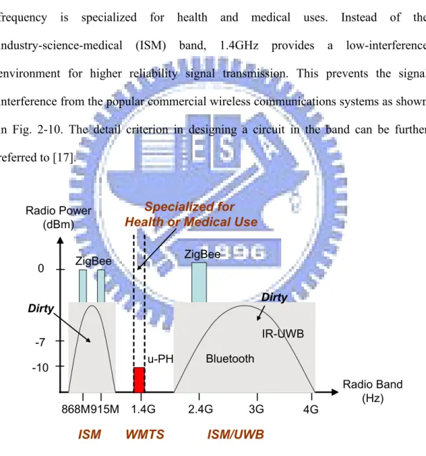
First, the radio frequency band is determined in the band 1.4GHz. This radio frequency is specialized for health and medical uses. Instead of the industry-science-medical (ISM) band, 1.4GHz provides a low-interference environment for higher reliability signal transmission. This prevents the signal interference from the popular commercial wireless communications systems as shown in Fig. 2-10. The detail criterion in designing a circuit in the band can be further referred to [17]. Radio Band (Hz) -10 -7 Specialized for Health or Medical Use
ZigBee u-PHI Radio Power (dBm) 2.4G 1.4G 3G 915M 868M 0 4G ZigBee Dirty Dirty Bluetooth IR-UWB WMTS ISM/UWB ISM
Sensor Node Compression/ Encryption QPSK Mapper Conjugate-Symmetric Subcarrier Spreading IFFT
P / S DAC RF 4 Digital Shaping Filter { User Spreading Code }
Fig. 2-11. Brief uPHI block diagram in a WSN
The system block diagrams in a transmitter are depicted in Fig. 2-11 that modulates signals according to the multi-tone CDMA (MT-CDMA) scheme [19]. The body signals come from a WSN. Depending on variant application requirements, an optional data compression or encryption could be added in signal processing. For the WBAN applications, it is required to have extreme low power consumption in a transmitter because a transmitter is made as small as possible for wearability, and is usually energy and battery limited. To achieve this goal, a function block of conjugate-symmetric subcarrier spreading is added to reduce the two-path transmission circuits (in-phase and quadrature-phase paths) to a single-path one. For example, assume the input subcarriers to an inverse fast Fourier transformation (IFFT) has the form of
} , ,..., , 0 , ,..., , , 0 { * 1 2 / * 2 2 / * 1 1 2 2 / 1 2 / + + − − = dN dN d d dN dN S (2-1)
where d is the frequency-domain subcarrier and N is the IFFT block size. So, it is derived that } Re{ } {S s IFFT s= N = (2-2)
In other words, every input pattern with the form of Eq. (2-1) results in a zero imaginary part of the IFFT output. This equivalently saves one path of DAC and RF
reduced. Those subcarriers in set S are duplicated one time, and this is also considered as spectrum spreading with spreading factor two. In a constellation mapper, it modulates signals into QPSK, and a higher order modulation more than 16-QAM is undesired in the system to prevent from the peak-to-average-power ratio (PAPR) problems. Considering the robustness to a fading channel and PAPR problems, a 16-point IFFT is used for OFDM modulation. The guard interval with 1/8 OFDM block size is applied prior to each OFDM symbol. Therefore, the system achieves the equalization ability to a fading channel. This low-order constellation mapper and small block size IFFT reduce the PAPR problem with the aid of digital reduction techniques [20][21] to achieve mild signal distortion and low out-of-band spurious interference. Then the IFFT output is spread by the spreading code and sent to a DAC. Finally, the word-length of DAC circuit decides the computation complexity and system performance. The packet format applied to the uPHI platform is illustrated in Fig. 2-12. In the beginning of a packet, there are ten periodic short preambles concatenated for timing synchronization. In the middle of the packet is the body for frame synchronization. Finally is the payload part carrying the data information.
t1 t2 t3 t4 t5 t6 t7 t8 t9 t10 GI2 T1 GI Data 1 GI Data 2
Packet preamble
GI2 T2 ……
Long preamble Packet preamble
Fig. 2-12. Packet format of the uPHI platform
In the signal power spectrum, WMTS has strict radiation power intensity definition. In the low band, 608-614MHz, the maximum in-band and out-of-band electrical field strength is defined as 200mV/m and 200uV/m, respectively. In the high band, 1395-1400MHz and 1429-1432MHz, the maximum in-band and out-of-band
field strength is 740mV/m and 540uV/m, respectively. Both the high and low band has the field strength measured at a 3-meter distance. As a result, a signal spectrum mask is specified in Fig. 2-13. This equivalently defines the allowable bandwidth for baseband signal transmission, i.e. 3MHz. To meet this spectrum mask design challenge, the digital signals before DAC circuit are upsampled four times and applied to a digital shaping filter to balance the power and design challenges between the RF front-end and baseband circuits. Table 2-5 summarizes the features of the uPHI system, including the channel, modulation, and packet features.
TABLE 2-5. UPHI SYSTEM PARAMETER SUMMARY
Parameter Features
RF Band 1.4GHz WMTS band
Maximum Data Throughput 86kb/s
User Spreading Code Type Gold Code
Spreading Code Length 31
Spreading Code Chip Rate 3Mc/s
IFFT/FFT Block Size 16
Guard Interval Duration 20.6 us
Constellation Mapper QPSK
Coded bits per subcarrier 2
frequency (MHz) fc -42 dBr -64 dBr 1.5 2 2.5 -1.5 -2.5 -2 3MHz 0 dBr
Fig. 2-13. The designed spectrum mask for the WMTS band
2-2-4 WiBoC Specifications
The system behavioral scheme of WiBoC is shown in Fig. 2-14 based on the pure OFDM modulation scheme. Here we depict this operation for multi-user in a view of time axis. The body signals are gathered and transmitted from the WSNs. The CPN, which is integrated in a portable device such as a personal digital assistant (PDA), receives the human body signals from WSNs for ubiquitous monitoring. When the WSNs and CPN is activated, they are initially in a reset state. In the beginning of network establishment, the CPN waits for sign-in signals from possible WSN nodes. After all WSNs join this network, the CPN broadcasts frames to every WSN (downlink process) for timing and frequency synchronizations. After the network synchronization in the downlink process, each WSN starts to gather body signals and transmits to the CPN (uplink process). Finally, the CPN receives the body information from WSNs. The proposed communication system operates in 1.4GHz radio band, and occupies 5MHz bandwidth.
Time Sign in uplink Sign in uplink Broadcast (downlink) Data Inspection Reset Reset Reset WSN1 CPN WSN2
Fig. 2-14. Timing sequence for the WSN and CPN communications
Fig. 2-15 shows the downlink broadcast frame. The first two repeated short preambles are used for the symbol timing synchronization and the coarse CFO estimation. The following two GI are for the boundary detection. The subsequent two long preambles are used to perform channel estimation and further fine CFO estimation. In the end of the frame, concatenated SCO preambles are used to perform SCO estimations.
Uplink frame structure is shown in Fig. 2-16. The preambles and the data are scrambled into a frame. The first GI is composed of the repeated subset of long preambles. It is used to perform symbol timing synchronization and symbol boundary detection. The following two long preambles are used for channel estimation. The signal field indicates the number of OFDM symbols in this frame. The final part of the frame is the payload data. Table 2-6 reveals the WiBoC system features in terms of radio frequency, signals bandwidth, modulations, and frame durations. Note that a convolutional code is applied in this version to verify the coded performance in the WBAN applications. This convolutional code applies a generator polynomial (133,171) [7].
![Table 2-4 illustrates the main difference between the WBAN and other 802 standards [18]](https://thumb-ap.123doks.com/thumbv2/9libinfo/8597442.189987/41.892.136.757.430.973/table-illustrates-main-difference-wban-standards.webp)