有機薄膜電晶體後退火之影響研究
71
0
0
全文
(2) 有機薄膜電晶體後退火之影響研究 The Post-Annealing Effect on Organic Thin-Film Transistors. 研 究 生:施尹婷. Student:Yin-Ting Shih. 指導教授:陳方中. Advisor:Fang-Chung Chen. 國 立 交 通 大 學 光 電 工 程 學 系 顯 示 科 技 研 究 所 碩 士 論 文. A Thesis Submitted to Display Institute College of Electrical and Computer Engineering National Chiao Tung University In partial Fulfillment of the Requirements for the Degree of Master in Display Institute July 2007 Hsinchu, Taiwan, Republic of China. 中華民國九十六年七月.
(3) 有機薄膜電晶體後退火之影響研究 學生:施尹婷. 指導教授:陳方中博士. 國立交通大學 光電工程學系 顯示科技研究所. 摘 要. 在有機材料中,載子的傳遞主要是以載子躍遷的方式進行,遷移率受 限於元件製程中有機薄膜品質的好壞。較差的成膜品質會使得有機薄膜電 晶體之載子移動率無法有效提升,因此如何在元件製程中提升薄膜品質一 直是非常重要的議題。本研究之主要目的在於探討元件熱退火處理對有機 薄膜電晶體之元件特性的影響和元件效能改善的機制,並探討熱退火處理 如何影響有機半導體層-pentacene-之成膜品質。 實驗結果顯示,有機薄膜電晶體經由元件熱退火處理後,元件的遷移 率由原先的 0.42 cm2V-1s-1 提升至 0.8 cm2V-1s-1,其中的原因部分來自於熱退 火處理使得元件的通道電阻大幅下降。另外,透過原子力顯微鏡我們證明 pentacene 通道部分的晶界,在熱退火處理後有減少的趨勢,我們推測這是 造成通道電阻下降的主因。然而,熱退火處理卻使得元件的接觸電阻和半 導體層中垂直於通道部分的電阻上升了。其內部機制,我們也進一步由原 子力顯微鏡和 X 光繞射儀的分析結果來探討。另外,我們也發現當我們結 合 poly-α-methylstyrene 表面修飾及元件後退火效應,可以使得元件的 interface traps 大幅下降,而且 pentacene 和基板表面的附著變的更好,進而 使得元件遷移率由 0.11 cm2V-1s-1 提升到 0.8 cm2V-1s-1。. i.
(4) The Post-Annealing Effect on Organic Thin-Film Transistors. Student:Yin-Ting Shih. Advisor:Dr. Fang-Chung Chen. Institute of Display National Chiao Tung University. ABSTRACT. Charge transport in organic semiconductor is typically described by hopping of charges between localized states. For this type of transport, the charge carriers are easily trapped at the grain boundary or by the disorder and impurities around the grains, resulting in the limitation of organic thin-film transistors (OTFTs) device mobility. Therefore, how to improve organic thin film quality becomes a very important issue. Based on the principle of controlling the growth of pentacene film, the effect of post-annealing treatment on pentacene-based TFTs is investigated in this study. Aims of our researches are to examine the effect of post-annealing treatment on device performance, pentacene crystal structures, and their correlations. It is found that the device mobility is increased from 0.42 to 0.80 cm2V-1s-1, which results from the reduced channel resistance. Images of atomic force microscopy (AFM) show that it is because the pentacene grain boundaries are reduced after thermal annealing. However, both contact and bulk resistances are slightly raised after post-annealing treatment. The mechanisms are further discussed by the investigation of the X-ray diffraction spectra and AFM patterns. In addition, the device mobility can be improved from 0.11 to 0.8 cm2V-1s-1 by combining PαMS modification and the post-annealing treatment. It is because that traps in pentacene/insulator interface are significantly moved and the adhesion between pentacene and insulator are improved.. ii.
(5) 誌. 謝. 本文能順利地完成全來自於顯示所的師長們、有機電子元件實驗室前輩們 及伙伴們的傾囊相助,在此由衷地表達我的感激。 首先要感謝我的指導教授—陳方中博士,在碩士班兩年中在研究上及學業 上給了我很多幫助,老師的建議及指導讓我在研究過程中更加順利。另外也要 感謝戴亞翔老師、黃乙白老師以及朱治偉博士在擔任口試委員的過程中給我的 寶貴建議,使得本文得以更加完善。 同時,我也要謝謝實驗室的祖榮學長、喬舜學長、志平學長,在研究知識 上傾囊相授,永昇學長、東賢學長以及立仁學長在實驗技巧的協助,他們帶領 我從無知中漸入佳境。另外,特別要感謝映頻學姐在 XRD 量測分析上的鼎力 相助,以及 MATLAB 程式上的貢獻,使我在實驗的分析過程中更加順利。也 謝謝 OTFT Group 的伙伴們:泰元、紓婷、曉芬、呈祥、昱仁、太獅,以及所 有的伙伴們,因為大家對實驗器材的維護和實驗時段的分享,才能讓實驗的過 程順利。也謝謝大家在生活上的分享,為枯燥的研究生活增添了許多樂趣。 最後,也要感謝我的家人在我求學過程中不斷地給我的鼓勵和生活上的支 持。沒有他們的大力相助,我的求學過程不可能如此平順。. 謹誌於 國立交通大學顯示科技研究所 中華民國九十六年七月 iii.
(6) CONTENTS. 要. ………………………..……………………. i. ABSTRACT. ………………………………………………. ii. 誌. 謝. ……………………………………………… iii. CONTENTS. ……………………………………………… iv. FIGURE CAPTIONS. ……………………………………………… vi. LIST OF TABLES. ……………………………………………… ix. 摘. Chapter 1 INTRODUCTION………………………..…………....... 1 1.1 General Statement of OTFT………………..………………… 1 1.2 Objective and Motivation……...…..………………………... 4 1.3 Organization of Thesis……………..………………………… 5 Chapter 2 LITERATURE REVIEW…………….……………………. 6 2.1 Organic Thin film Transistor………………………..……... 6 2.1.1 The Geometry and Operation…………………….…….. 6 2.1.2. The Parameters………………………………..……… 8. 2.1.3. Effective Resistance…………………………..……… 10. 2.2 Organic Semiconductor………………………………….…… 15 2.2.1 The Basic Structure of Pentacene……………..……… 15 2.2.2 Charge Transport……………………………..………. 16 2.3 The Thermal Annealing Treatment…………………..………… 18 Chapter 3 EXPERIMENTAL PROCESS……………..………..……... 21 3.1 Device Fabrication………………………………………........ 21 iv.
(7) 3.3.1. Substrate Cleaning……………………………….. 21. 3.1.2 The Surface Treatment of Insulator Surface………… 22 3.1.3 Pentacene and Gold Electrode Deposition…………… 23 3.1.4. The Post-Annealing Treatment………………………. 23. 3.2 Device Measurement System………………………………… 26 Chapter 4 THEOREM & ANALYSIS METHOD…………………... 27 4.1 Morphology of Pentacene Thin Films…………………………. 27 4.2 Pentacene Crystal Structure……………………………………. 29 4.2.1 Pentacene Phase - From Bragg’s Law…………………. 29 4.2.2 Pentacene Crystal Size - From Scherrer Equation……... 31 4.2.3 Pentacene Crystalline - From Paracrystal Theory……. 32 Chapter 5 RESULTS & DISCUSSION…………………………………. 33 5.1 The Effect on Pentacene Crystal…………………………….…. 33 5.1.1 The Analysis of Film Morphology…………………….. 33 5.1.2 The Analysis of XRD spectra………………………..… 36 5.2 The Effect on Device Property………………………………… 39 5.2.1 Electrical Characteristics………………………………. 39 5.2.2. Resistance Analysis……………………………….…… 42. 5.2.3 DC Stress Degradation…………….…………………… 45 5.3 Trap Calculation………………………………………………... 47 5.3.1 Grain Boundaries………………………………………. 47 5.3.2 Interface………………………………………………... 48 5.3.3 Summary……………………………………………….. 50 Chapter 6. CONCLUSIONS……………………………………………… 51. REFERENCES …………….…………….………..………….…………… 53 APPENDIX. …………………….……………..…..…………………… 59 v.
(8) FIGURE CAPTIONS. Chapter 1 1.1 Evolution of hole-mobility for the most common p-type organic semiconductors. The mobility has been improved by more than five orders of magnitude during 15 years……………………………………..................................................................... 2 1.2 The first full-color active-matrix organic LED display on a flexible plastic substrate developed by SONY Corp. (Picture source: http:// www. etimes.com/showArticle.jhtml?articleID=199703004)............................................... 2. Chapter 2 2.1 (a) top-contact structure of OTFT and (b) bottom-contact structure of OTFT. In the top-contact device, the organic semiconductor is deposited before the deposition of metal electrodes. On the contrary, the deposition sequence of bottom-contact device is reversed…………......................................................................................... 7 2.2 A typical plot of drain current (ID) versus drain voltage (VDS) at various gate voltages (VGS). ID linearly increases with VDS in the linear regime; however, ID tends to be independent of VDS in the saturation regime…………………………….. 8 2.3 Semi-logarithmic plot of ID versus VGS (left y-axis) and plot of |ID|1/2 versus VGS (right axis) at a constant drain voltage of 60 V (saturation regime)………………………………………………………………………............. 10 2.4 Total resistance as a function of L at different VGS. By the TLM, RC is given by the intercept of the total resistance Ron versus L plot at L = 0…………………………... 11 2.5 The equivalent circuit of top-contact OTFT near the pentacene and electrode interface. The rch, rbulk, and rc are calculated by the theorem which published by Michael Shur in 1990.…………………………………………………….................. 12 2.6 Chemical structure of pentacene (C14H22). It is a rod-like aromatic molecule composed of five benzene rings………………………………...…………................ 15 vi.
(9) 2.7 Charge transport in solids. (a)Band transport. The band of a perfect crystal is described as a straight line where the delocalized free carrier moves. (b) Hopping transport. In this type of transport the carrier is localized due to disorder, defects o self-localization (e.g. polarons) and hops from site to site with the essential help of lattice vibrations……………………………………………………………………... 17 2.8 Arrhenius plot of the logarithm mobility versus the reciprocal temperature………... 19. Chapter 3 3.1 The procedure of substrate cleaning. The SiO2 wafers were placed on the Teflon carrier during the cleaning process………………………………………………….. 21 3.2 The chemical formula of poly-α-methylstyrene (PαMS). Our SiO2 surface was modified with PαMS by spin-coating from toluene solutions…………...………… 22 3.3 The flow chart of device fabrication. To discuss the effect of post-annealing, a portion of our devices were treated by thermal annealing process after device fabrication……………………………………………………………........................ 25. Chapter 4 4.1 (a) The Rrms of this AFM image is 7.599 nm , which was obtained by analyzing over 3×3 μm2 area using the built-in software of the AFM. (b) The grain boundaries defined by a program of MATLAB. The detail of the program is shown in APPENDIX……………………………………………………………………….. 28 4.2 The XRD spectrum for 60-nm thick of pentacene thin films. There are five intensity-peaks, (00l), l = 1, 2, …, 5………………………………………………... 30. Chapter 5 5.1 5-nm pentacene thin films for (a) as-prepared and (b) thermally annealed samples………………………………………………………………………………. 34 5.2 20-nm Pentacene thin films (a) as-prepared, (b) after thermal annealing. 30-nm thick samples (c) as-prepared, (d) after thermal annealing. 60-nm thick samples (e) as-prepared, and (f) after thermal annealing………………………………………… 35 5.3 The XRD spectra obtained from 60 nm-thick pentacene films. The inset shows the XPS spectrum near (002) intensity peak…………………………..………………… 37 vii.
(10) 5.4 (δs)02 as a function of the fourth power of the diffraction order m4. From the intercept and slope of this plot, we can obtain the mean crystal size vertical to substrate and second kind of distortion of crystal structure……………….………… 37 5.5 The current-voltage characteristics of pentacene-based TFT with anneal/ un-annealed condition. (a) The drain current ID versus the drain-source voltage VDS at VGS =60 V and (b) the absolute value of the drain current and the logarithmic drain current versus the gate-source voltage VGS at VDS =60V. The post-annealing treatment was carried out at 90 oC for 80 min in a N2-filled glove box…………………………………………………………………………………… 41 5.6 The simplified equivalent OTFT circuit, where the conducting path is divided into three parts of resistance, rch, rC, and rbulk……………………………………………. 42 5.7 Resistance characteristics of pentacene-based TFT with/without the annealing treatment. (a) the channel resistance versus gate voltage VGS and (b) the effective series resistance versus VGS. In our assumption, effective contact rersistance rC is VGS independent and effective bulk resistance rbulk is variable with VGS. The effective series resistance is equal to the sum of rC and rbulk………………………...……………………..………………………………….. 43 5.8 The DC stress of the pentacene-based TFTs. The continuous DC voltage bias was VGS = 30 V lasting for 2500 sec……………...……………………………………… 46 5.9 Levinson plot of “ln(ID/VGS) vs. 1/VGS” for our devices. For these two samples, the trap density at the grain boundary can be estimated by the slope of this diagram………………………………………………………………........................ 48. viii.
(11) LIST OF TABLES. 2.1. The related researches about thermal annealing treatment………………………… 19. 5.1. The analysis of XRD spectra………………………………………………………. 38. 5.2. The device performance…………………………………………………………… 39. 5.3. The key parameters of devices…………………………………………………….. 45. 5.4. The parameters of devices with/without surface treatment…………………........... 49. ix.
(12) Chapter 1. INTRODUCTION. 1.1 General Statement of OTFT. In recent years, the research of organic materials grows rapidly because of their high potential for the applications on optoelectronic and electronic devices, such as photovoltaic cells [1-2], organic light-emitting diodes [3], organic thin-film transistors [4], nonlinear optical materials, etc. More and more optoelectronic devices tend to be fabricated based on organic materials due to many advantages, such as flexibility, low-cost and large-area devices. Recently, organic thin-film transistors (OTFTs) have attracted intensive attention due to the significant improvement in mobility which reaches higher than 1 cm2V-1sec-1 [5-8]. The state-of-art device mobility reported so far is even up to 35 cm2V-1sec-1. [9] The development history of p-type OTFTs are shown in Figure 1.1 [4]. Apparently, pentacene is the most promising organic semiconductors applied in p-type OTFTs because pentacene exhibits high device performance comparable to that of hydrogenated amorphous silicon (α-Si:H). SONY Corp. even has developed the first full-color active-matrix organic light-emitting diode display on a flexible plastic substrate as shown in Figure 1.2. The semiconductor used in the transistors of this organic LED display is exactly pentacene.. 1.
(13) Figure 1.1. Evolution of hole-mobility for the most common p-type organic. semiconductors. The mobility has been improved by more than five orders of magnitude during 15 years.. Figure 1.2. The first full-color active-matrix organic LED display on a flexible plastic. substrate developed by SONY Corp. (Picture source: http://www.eetimes.com/showArticle.jhtml?articleID=199703004). 2.
(14) Unlike the inorganic crystals which are formed by atoms with covalent bonds, the structure of organic materials is formed by molecules weakly bonded by van der Waals force. It is much weaker than the covalent force in inorganic materials, which is the reason for their low mobility. The conducting mechanism in organic semiconductors is quite different from that in metals or conventional semiconductors. Because organic semiconductors consist of chemically conjugated systems, charge transport is typically described by hopping of charges between localized states. In this type of transport, the charge carriers are localized due to the structure disorder, defects or self-localization (polarons). Furthermore, the mobile charges are easily trapped at the grain boundary or by the disorder and impurities around the grains, resulting in the limitation of the device mobility. Pentacene is a well-known the organic semiconducting materials. The mobility of pentacene-based TFTs is relatively high since pentacene has a strong tendency to form an ordered film. However, the film quality is deeply affected by the growth conditions, such as deposition temperature, evaporation rate, base pressure, surface roughness, etc. Each condition mentioned above plays an important role in the property of film morphology; however, it is very difficult to control the deposition condition. [10-11] Therefore, an easier way to improve film quality is necessary.. 3.
(15) 1.2 Objective and Motivation. Although the device performance of OTFTs is still not good enough, the flexible property of organic materials creates the superiority of organic semiconductors over the inorganic semiconductors for applications. Therefore, how to enhance the device performance of OTFTs was always interested. As mentioned in the preceding section, it has been shown that the formation of pentacene films is significantly sensitive to the growth conditions, and the film quality plays an important role on device performance. Consequently, to understand and, further, to control of molecular growth become crucial issues. Post-annealing treatment is a simple method to improve the film quality. Several reports have investigated the post-annealing effect on the pentacene thin-film and device characteristics. [12-14] However, the detailed mechanism is still not well understood yet. In this work, the effect of the post-annealing treatment on pentacene-based TFTs is investigated systematically. We firstly controlled the growth of pentacene through the post-annealing treatment, followed by studying the correlation between the thin-film morphology of pentacene and TFT device performance. The details are as following issues: (1) the effect of post-annealing treatment on device performance, (2) the effect of post-annealing treatment on pentacene crystal structures, and (3) their connections.. 4.
(16) 1.3 Organization of Thesis. The thesis consists of six chapters. In this chapter, our objective and motivation have been described. In chapter 2, we have introduced the background knowledge of this thesis, including the operation and the parameters of OTFTs, the concept of charge conduction in organic semiconductor, and so on. Moreover, we also present an overview of related researches on thermal annealing effect and its device performance. Chapter 3 gives a detailed description of our device fabrication process and measurement system. In chapter 4, the analysis methods are introduced. It describes how we analyzed the grain boundary density and roughness from images recorded by atomic force microscopy, and how we examined pentacene phase and crystal structure from X-ray diffraction-spectra. Chapter 5 shows our experimental results as well as the related details Conclusions and future work are summarized in chapter 6.. 5.
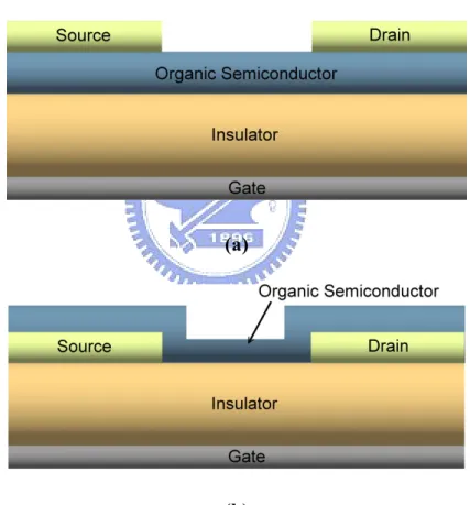
(17) Chapter 2. LITERATURE REVIEW. 2.1 Organic Thin film Transistor [4]. 2.1.1. The Geometry and Operation. Figure 2.1 (a) and 2.1 (b) show two structures of OTFTs that are most commonly used, top-contact and bottom-contact structures. In the top-contact device, the organic semiconductor is deposited before the deposition of metal electrodes. On the contrary, the deposition sequence of bottom-contact device is reversed. Pentacene-based TFTs exhibit p-type device behavior, which means that the holes serve as majority carriers. Therefore, a negative bias of gate voltage was applied to accumulate holes in the p-type active layer. The operation of a p-type OTFT can be simply described as following:. (1) When the gate bias VGS is zero, there is no gate-induced charge near the semiconductor/insulator interface. At this moment, no charges can transport even if a small negative source-drain bias VDS is applied, since there are no mobile charges in the organic semiconductor.. (2) When a negative VGS is applied on gate electrode, accumulation of positive charges at the semiconductor/insulator interface takes place and an electric field. 6.
(18) is induced. This is the accumulation regime. In this regime, the accumulation of charges will form a channel from source to drain electrodes, which allows hole current to flow inside.. (3) While the electric field is large enough and under an negative bias of VDS, the hole current is induced in the channel and subsequently flows from the drain to the source electrode.. (a). (b) Figure 2.1. (a) top-contact structure of OTFT and (b) bottom-contact structure of OTFT.. In the top-contact device, the organic semiconductor is deposited before the deposition of metal electrodes. On the contrary, the deposition sequence of bottom-contact device is reversed.. 7.
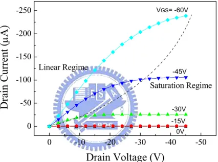
(19) 2.1.2. The Parameters. The current (I) −voltage (V) characteristics model of OTFTs are often expressed as that of convection inorganic semiconductors devices. Figure 2.2 shows a plot of drain current (ID) versus drain voltage (VDS) at various gate voltages (VGS).. Drain Current (μA). -250. VGS= -60V. -200 -150 Linear Regime. -45V. -100. Saturation Regime. -50. -30V -15V. 0. 0V. 0. -10. -20. -30. -40. -50. Drain Voltage (V) Figure 2.2. A typical plot of drain current (ID) versus drain voltage (VDS) at various gate. voltages (VGS). ID linearly increases with VDS in the linear regime; however, ID tends to be independent of VDS in the saturation regime.. At low VDS, i.e., − V DS << −(VGS − VT ) , ID increases linearly with VDS, which is called linear regime. In this regime, ID is approximately described as the following equation:. 8.
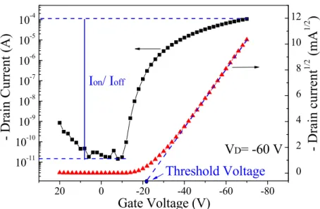
(20) ID =. WCi V μ (VGS − VT − DS )VDS L 2. (2.1). where W is the channel width, L is the channel length, μ is the field-effect mobility, VT is the threshold voltage, and Ci is the capacitance per unit area. At large VDS, i.e., − V DS > −(VGS − VT ) , ID tends to saturate due to the pinch off of accumulation layer, which is called saturation regime. The characteristics of the saturation current are expressed by the equation:. ID =. WCi μ (VGS − VT ) 2 L. (2.2). Figure 2.3 shows Gate voltage dependence of Drain current. The mobility (μ) discussed in this study is extracted from the slope of the plot of |ID|1/2 versus VGS in the saturation regime, according to ID =. WCi μ (VGS − VT ) 2L. (2.3). The threshold voltage (VT) defines the onset voltage for the channel formation. VT shown in Equation (2.3) represents the x-intercept of |ID|1/2-VGS plot in the saturation regime. The on-off current ratio (Ion/Ioff) which means the ratio of the current turned device on over the current turned device off is also exhibited in Figure 2.3. Further, the sub-threshold swing (S.S.) reveals how fast the device can be turned on and off, defined as S .S . =. ∂VG ∂ (log I D ). (2.4). 9.
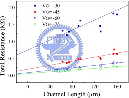
(21) 10. -7. 8. Ion/ Ioff. 10. -8. 6. -9. 4. 10 10. -10. 10. VD= -60 V. -11. 10. Threshold Voltage 20. Figure 2.3. 0. -20. -40. Gate Voltage (V). -60. 2. 1/2. (mA ). 10. -6. 1/2. - Drain Current (A). -5. 10. - Drain current. 12. -4. 10. 0. -80. Semi-logarithmic plot of ID versus VGS (left y-axis) and plot of |ID|1/2 versus. VGS (right axis) at a constant drain voltage of −60 V (saturation regime).. 2.1.3. Effective Resistance. The approach utilized to discuss resistance of OTFT is the transmission-line method (TLM). [15] The concept of TLM was described in Figure 2.4. Based on the TLM, we separate the whole device resistance (Ron) of OTFT into a total contact resistance (RC, source/drain contacts) and channel resistance (RCh). At low VDS, RCh is a function of L and VGS. Therefore, the RC is given by the intercept of Ron versus L plot at L = 0, where Ron = RCh + RC. But this assumption is not very critical. One of the reasons is that the RC we obtained is the contact resistance at L=0 without taking the whole source/drain contact area into account. Besides, it is invalid to multiply RC by source/drain contact area since. 10.
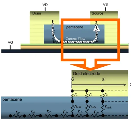
(22) the distribution of the current is not uniform throughout the whole source/drain contact area. Another reason is that RC is not the pristine contact resistance because the resistance comprises the resistance of contact surface and the resistance of bulk pentacene vertical to the channel, as shown in Figure 2.5. Accordingly, the influence of contact resistance and bulk resistance should be discussed individually.. VG= -30 VG= -45 VG= -60 VG= -75. Total Resistance (ΜΩ). 2.0 1.5 1.0 0.5 0.0 0. 40. 80. 120. 160. Channel Length (μm) Figure 2.4. Total resistances as a function of L at different VGS. By the TLM, RC is given. by the intercept of the total resistance Ron versus L plot at L = 0.. To obtain accurate contact resistance and bulk resistance, we followed the theorem which published by Michael Shur in 1990. [16-17] M. Shur’s theory is based on TLM and followed by a second order differential equation to calculate effective resistance. 11.
(23) and injection length. According to his theorem, in the linear regime, the Ron can be expressed as the sum of the intrinsic channel resistance (rch) which is independent of L, and the parasitic resistance (Rp), as the following equation:. ∂V Ron = DS ∂I DS. vg. = vds →0. L + RP = rch L + R p Wμ i Ci (VG − VT ). (2.5). where μi is the intrinsic mobility and VT is the threshold voltage. In Figure 2.5, a simple schematic circuit diagram at the source contact of OTFT is illustrated.. Figure 2.5. The equivalent circuit of top-contact OTFT near the pentacene and electrode. interface. The rch, rbulk, and rC are calculated by the theorem which published by Michael Shur in 1990. [16-17]. 12.
(24) The current distribution under a contact surface can be described from the following equation: dI ch ( x) = −WJ c ( x), dx. (2.6). where Ich(x) specifies the current parallel to the channel, x represents the coordinate in the direction parallel to channel, and Jc is the vertical current density, J c ( x) = Vch ( x) / rP. (2.7). Here Vch(x) is the electrical potential of channel at position x and rP is the effective parasitic resistance consist of effective contact and bulk resistance. rP = rbulk + rC. (2.8). The variation of Vch(x) along x can be expressed as dVch ( x) = − I ch ( x)rch dx. (2.9). where rch is the channel resistance of the pentacene film and W is the contact width. Combing Equations (2.6) and (2.9), we have a second order differential equation as: d 2Vch ( x) Vch ( x) = dx 2 ( LT ) 2. (2.10). where. ⎛ r LT = ⎜⎜ P ⎝ Wrch. ⎞ ⎟⎟ ⎠. 1/ 2. (2.11). is the effective transfer length. The boundary conditions for Equation (2.10) are. 13.
(25) dVch ( x) dx. x =0. dVch ( x) dx. x=d. = − I 0 rch. (2.12). =0. (2.13). and. where I0 is the total channel current and d is the contact length. By solving the Equation (2.10) with boundary conditions of Equation (2.12) and (2.13), we get. LT = RP / rch ,. (2.14). From Equation (2.10), we can obtain the effective contact resistance, rCeff = WL2T rch = WRP2 / rch. (2.15). 14.
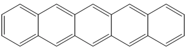
(26) 2.2 Organic Semiconductor. 2.2.1. The Basic Structure of Pentacene. Pentacene (C14H22) is a rod-like aromatic molecule composed of five benzene rings. (see Figure 2.6) [18] Benzene consists of a chemically conjugated system in its molecular structure, which is a system of carbon atoms covalently bonded with alternating single and double bonds. In a conjugated molecule the electrons in the. π-bond can be excited while the electrons in the σ-bonds in the backbone maintain the structural integrity of the molecule, hence a conjugated polymer can be electronically excited without being destroyed. Moreover an electron (or hole) in a conjugated system will be delocalized within the conjugated segment. Therefore, the conduction mechanism in organic semiconductors is very different from that in metals or inorganic semiconductors. The carrier mobility is strongly dependent on the molecular structure and ordering. On the other hand, compared with other organic semiconductors, pentacene exhibits a strong tendency to form highly ordered films, which depend on the surface properties of substrates and the growth conditions. [10]. Figure 2.6. Chemical structure of pentacene (C14H22). It is a rod-like aromatic molecule. composed of five benzene rings.. 15.
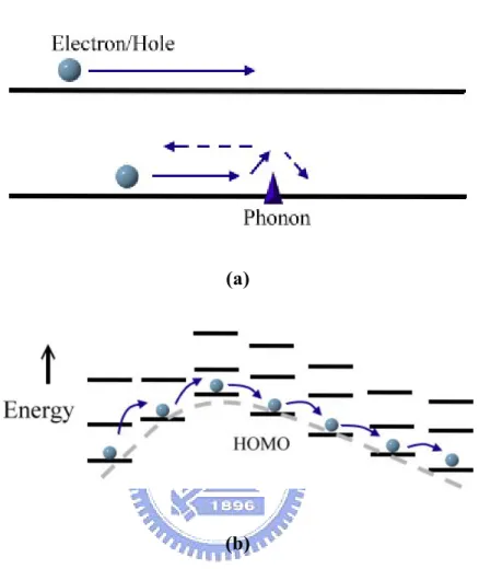
(27) 2.2.2. Charge Transport [19-21]. The conducting mechanism in inorganic semiconductors or metals is usually described by band transport. No matter how perfect the crystal is, the symmetry is always disrupted by phonons (lattice vibrations) that scatter the charge carriers. The diagram is shown in Figure 2.7 (a). Since less phonon are generated at lower temperature, the mobility of the charge carriers decreases with increasing temperature. It is mentioned that organic semiconductor consist of a chemically conjugated system. This system results in a general delocalization of the electrons across all of the adjacent parallel aligned π-orbital of the atoms. Further, the structures of organic semiconductor are usually disordered, and the energy bands formed by extended conjugated chains are usually not very long and separated by defects. Those defects also create traps for charges; and hence the mobile charges are fairly localized. Because of defects and disorder, organic semiconductors have no extended band structures as inorganic semiconductors. Charge transport in organic semiconductors is typically described by hopping of charges between localized states, which is a phonon assisted mechanism from site to site as shown in Figure 2.7 (b). In this type of transport the carrier is localized due to disorder, defect or self-localization (polarons). In summary, the charge transport mechanism in organic semiconductor is thermally activated hopping at high temperature. In some cases, it becomes band-like transport described by the band like a straight line at very low temperature. [22]. 16.
(28) (a). (b) Figure 2.7. Charge transport in solids. (a)Band transport. The band of a perfect crystal is. described as a straight line where the delocalized free carrier moves. (b) Hopping transport. In this type of transport the carrier is localized due to disorder, defects o self-localization (e.g. polarons) and hops from site to site with the essential help of lattice vibrations.. 17.
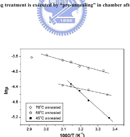
(29) 2.3 The Thermal Annealing Treatment. Thermal annealing is a heat treatment of material, usually changing its orderings or properties. The annealing process contains heating and maintaining at a suitable temperature, and then cooling. It is hoped to improve the molecular structure and the properties of devices. Therefore, the thermal annealing effect on film orderings and the relationship between molecular structure and device properties are concerned. The thermal annealing treatment has been widely used in the fabrication of poly-Si TFTs [23-24]. Since 2002, several researches about thermal annealing effect on OTFTs and organic films have been proposed. The related literatures are summarized in Table 2.1, including device structures, annealing conditions, and device mobility. Researches on pentacene thin film and its device performance have been concerned. In Figure 2.8, the plot of ln(μ) versus 1000/T can be fitted by the Arrhenius formula:. ⎛ Ea ⎞ ⎟ ⎝ kT ⎠. μ ∝ μ 0 exp⎜ −. (2.16). indicating that the charge transport in devices can be described by the hole-hopping model. [27, 30]. 18.
(30) Table 2.1. The related researches about thermal annealing treatment.. Authors. Device Structure. Best. Mobility. G\insulator\semiconductor\S.D. Annealing Condition. cm2/Vs. T. Komoda et al.. [25] n+-Si\SiO2\pentacene\Gold. 50 οC/1 hr (in vacuum). 0.2. S. J. Kang et al.. [13] n+-Si\SiO2\pentacene\ Gold. 90 οC/1 hr (in vacuum)*. 0.49. 140 οC/12 hr (in N2). 0.56. 40-120 οC/1 hr (in vacuum). /. R. B. Chaabane et al. [29] Si\SiO2 + Si3N4\NiPc\Gold. 100 οC/1 hr (in vacuum). 8.9×10⁻³. [30] n+-Si\SiO2\pentacene\ Gold. 45 οC/2 hr (in vacuum). ≒0.22. T. Seckitani et al. R. Ye et al.. [26-28] [12]. D. Guo et al.. Au\Polyimide\pentacene\ Gold n+-Si\SiO2\pentacene. * The annealing treatment is executed by “pre-annealing” in chamber after pentacene deposition.. Figure 2.8. Arrhenius plot of the logarithm mobility versus the reciprocal temperature. [30]. 19.
(31) In ref. [12, 13, 25], both AFM images and XRD analysis showed that pentacene ordering were improved by thermal annealing. Nevertheless, the mechanism has not been explained in details. How the device performance was influenced by the thermal annealing treatment was still not well understood yet. Therefore, to understand the mechanism of the post-annealing effect on OTFTs is the most important target in this study.. 20.
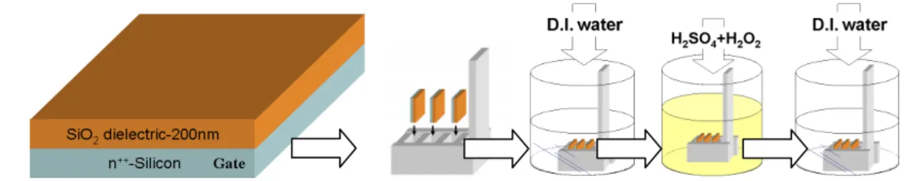
(32) Chapter 3. EXPERIMENTAL PROCESS. 3.1 Device Fabrication. 3.1.1. Substrate Cleaning. The substrate used in this study consists of heavily n-doped silicon wafer with 200 nm-thick thermal oxides. To remove organic contaminants, the substrates were rinsed in de-ionized water for 5 minutes, dipped in H2SO4 + H2O2 (H2SO4:H2O2=3:1, 80 οC) solution for 20 minutes, and then rinsed in de-ionized water for another 10 minutes. Finally, the cleaned substrates were blew by dry N2 gas and dried in an oven at 120 οC for 1 hour.. Figure 3.1. The procedure of substrate cleaning. The SiO2 wafers were placed on the. Teflon carrier during the cleaning process.. 21.
(33) 3.1.2. The Surface Treatment of Insulator Surface. Surface treatment on the gate insulator is one of the effective methods to control the condition of dielectric surface. The treatment has been proposed to have significant effects on the resulting thin film structure and electrical characteristics. [31] Therefore, surface treatment on the SiO2 is carried out prior to the deposition of the pentacene layer. Our SiO2 surface was modified with poly-α-methyl styrene (PαMS, Aldrich Co.) by spin-coating from toluene solutions, which can change the electronic state at the dielectric/channel interface, and improve the pentacene-based TFT performance. After spin-coating, the PαMS modified substrates were baked at 100 oC for 1 hour to remove residual solvent. The PαMS film was about 8-nm-thick, and the capacitance per unit area Ci of 200 nm-thick thermal oxides with PαMS-coating layer is 1.41 × 10⁻⁸ F/cm2 in our study.. Figure 3.2. The chemical formula of poly-α-methyl styrene (PαMS). Our SiO2 surface. was modified with PαMS by spin-coating from toluene solutions.. 22.
(34) 3.1.3. Pentacene and Gold Electrode Deposition. The growth of pentacene thin film and deposition of gold electrodes were accomplished via vacuum sublimation by thermal evaporation. In the chamber, a quartz oscillator and a shutter were utilized to control the deposition rate avoiding deposition under unstable vapor flux. The deposition temperature was measured by an Al-Cr thermocouple. The pentacene source was placed in a BN-crucible and heated by a W-coil, and gold ingot was placed and heated in a W-boat. The substrates were attached to shadow masks to define the deposited area. The 60 nm-thick pentacene (FLUKA Co., without further purification) thin-films were deposited under a working pressure below 1.6 × 10⁻⁶ Torr. During the thin film formation, the deposition rate was maintained at 0.05 nm/s, and the substrate temperature was kept at 17 oC. Gold, as the source/drain electrode, was finally evaporated on top of the pentacene thin-film through a patterned shadow mask. The channel width (W) was 2 mm and the channel length (L) ranged from 75 to 160 μm. The device fabrication procedure is shown in Figure 3.3.. 3.1.4. The Post-Annealing Treatment. To discuss the effect of post-annealing, a portion of our devices were treated by the thermal annealing process. The thermal annealing treatment was carried out at 90 oC for. 23.
(35) 80 min in a nitrogen-filled glove box. The concentrations of O2 and H2O in the glove box are both controlled bellow 1 ppm. After thermal annealing, the annealed samples are then cooled down naturally.. 24.
(36) STEP 1 Surface modification on cleaned substrates with PαMS by spin-coating from toluene solutions.. STEP 2. Pentacene thin film deposition through shadow mask.. STEP 3. Golden electrode deposition through shadow mask.. Device fabrication complete.. Figure 3.3. The flow chart of device fabrication. To discuss the effect of post-annealing, a. portion of our devices were treated by thermal annealing process after device fabrication.. 25.
(37) 3.2 Device Measurement System. After completing the experimental process and before measuring the samples, all of our samples were conserved in the vacuum environment to avoid exposure to moisture and oxygen. The current−voltage characteristics of this study were measured at room temperature under the atmosphere by a probe station connected with the Keithley 4200−SCS semiconductor parameter analyzer in a dark room. In the ID-VD measurement, the drain bias was swept from 0 to -45 Volts and the gate voltage step were 0, −15, −30, −45, and −60 Volts, respectively. In the ID-VG measurement, the gate bias ranged from +10 to −60 Volts, and the drain voltage step were 0, −15, −30, −45, and −60 Volts. To investigate into the effective contact resistance, the ID−VD curve was measured by small drain bias sweeping from 0 to −1 Volts and the step at each volt of gate voltage ranging from 0 to −90 Volts.. 26.
(38) Chapter 4. THEOREM & ANALYSIS METHOD. 4.1 Morphology of Pentacene Thin Films. In our study, the crystal structure and morphology properties of pentacene thin film were investigated by using atomic force microscopy (AFM) and X-ray diffraction (XRD). In this chapter, the analysis methods of AFM images and the theorems of XRD-spectra analysis were investigated. The characterization of the surface morphology of pentacene thin film was examined by AFM (Digital Instruments NanoScope Dimension D3100 probe microscope system). Each of our images was recorded in tapping mode in air with 1 Hz of scan rate and 256×256 dpi. To examine the post-annealing effect on pentacene grain in channel, in bulk, and in contact area, we prepared pentacene thin-film samples with different thickness: 5, 10, 20, 30, and 60 nm. The value of root-mean-square roughness (Rrms) of film was obtained by analyzing over 3×3 μm2 area using the built-in software of the AFM instrument. Figure 4.1 displays one of the surface morphology from our samples, and a Rrms of 7.599 nm is obtained. Moreover, a program of MATLAB was used to calculate the density of grain boundary. The grain boundaries defined by the program were shown in the Figure 4.1 (b), and the density of grain boundary is 3.92. 27.
(39) (μm)-1.. (a). (b) Figure 4.1. (a) The Rrms of this AFM image is 7.599 nm , which was obtained by analyzing. over 3×3 μm2 area using the built-in software of the AFM. (b) The grain boundaries defined by a program of MATLAB. The detail of the program is shown in APPENDIX.. 28.
(40) 4.2 Pentacene Crystal Structure [5]. The characterization of our pentacene thin film structure was investigated by XRD, which is the direct evidence for the periodic atomic structure of crystals. The specification of XRD is M18 XHF, MacScience. The XRD measurements were performed to 60-nm thick pentacene thin films, and it was operated with Cu-Kα (λ = 1.5406 Å) radiation in a symmetric reflection, coupled θ−2θ mode. Phase identification using XRD relies mainly on the positions of the peaks in a diffraction profile and to some extent on the relative intensities of these peaks. The shapes of the peaks, however, contain additional and valuable information. The shape, particularly the width, of the peak is a measurement of the amplitude of thermal oscillations of the atoms at their regular lattice sites. It can also be a measurement of vacancy and impurity element concentrations and even plastic deformation, any factor which results in a distribution of d-spacings. In the following sections, we will discuss about how we analyze our XRD data.. 4.2.1. Pentacene Phase - From Bragg’s Law. The principle of diffraction is described by Bragg’s law, which refers to the simple equation: nλ = 2d hkl sinθ hkl. (4.1). Intensity-peaks represent multiple lattice spacings (d), which can be labeled as (hkl) peaks. Each dhkl corresponds to a specific angle (θhkl). λ is the wavelength of the. 29.
(41) incident X-ray beam, and n is an integer. A XRD-spectrum consists of the position (2θ) and the intensity of (hkl) peaks. The former implies some information about crystal structures such as size and sharp, and the latter reveals what kind of atoms are included in a film and how these atoms arrange. One of our pentacene X-ray diffraction (λ = 1.5406 Å) spectra is shown in Figure 4.2. Five intensity-peaks represent multiple dhkl. According to the Bragg’s law, (001) peak at 5.7o corresponds to d001 with value of 15.49 Å.. (001). Intensity (a. u.). (002). (003) (004). 5. 10. 15. 20. 25. (005) 30. 2θ (deg.) Figure 4.2. The XRD spectrum for 60-nm thick of pentacene thin films. There are five. intensity-peaks, (00l), l = 1, 2, …, 5.. Similar result has been reported by C.D. Dimitrakopoulos et al. The value of d001 was found to be 15.4 Å. [4] However, the expected [32-33] single-crystal structure of pentacene in triclinic with a = 7.90 Å, b = 6.06 Å, c = 16.01 Å, α = 101.9 Å, β = 112.6. 30.
(42) Å, and γ = 85.8 Å. In such a structure, the (001) plane spacing d001 is ∼14.5 Å. Obviously, the result of d001 = 15.49 Å is attributed to a phase different with single crystalline phase, called “thin film phase.” The other pentacene phase with (001) peak at 6.1ο is called “bulk phase,” which is closer to the (001) peak of single crystal phase at 6.25ο. Only (00l) peaks are found in pentacene XRD-spectrum with the absence of any other (hkl) peaks, which indicates that all the pentacene crystals in the film are oriented along their (00l) planes parallel to the substrate.. 4.2.2. Pentacene Crystal Size - From Scherrer Equation [34-35]. There are two ways to calculate pentacene grain size along c-axis, the Scherrer Equation and Paracrystal Theory. The crystallite size measured by the Scherrer method is given by Lhkl =. Kλ δθ hkl cosθ hkl. (4.2). Here Lhkl is the volume-weighted size, θhkl is the Bragg angle, λ is the wavelength of the X-ray, and K is unit cell geometry dependent constant whose value is typically between 0.85 and 0.99. δθ hkl is the full width of the peak at half maximum of Bragg’s peak intensity (FWHM) in radians.. 31.
(43) 4.2.3. Pentacene Crystalline - From Paracrystal Theory [36-39]. Paracrystal theory is another way used to calculate pentacene crystal size along c-axis. To use both methods to verify our results becomes reliable. From the formula of paracrystal theory,. π 4 g II4 4 1 (δs ) = (δs ) + (δs ) = 2 + 2 m , Lhkl d hkl 2 0. 2 c. 2 II. (4.3). we can obtain two important parameters, Lhkl and g II , from the intercept on the ordinate axis and the slope of the straight line determined by the least-squares fitting. Here Lhkl specifies the mean crystal size vertical to the plane (hkl), and g II represents the distance fluctuation between successive planes of the family (hkl) or second kind of distortion of crystal structure. Besides, (δs) c is the broadening associated with the size of the crystal domain, (δs) II stands for the broadening due to lattice distortions of the second kind, m is the 2 is the mean spacing between (hkl) planes. (δs ) 0 is order of the diffraction, and d hkl. the overall broadening excluding instrumental broadening and is further described by:. (δs ) 0 =. 2 cosθ hkl δθ hkl. (4.4). λ. where λ is the X-ray wavelength, θhkl is the diffraction angle and δθhkl represents the full width of the peak at half maximum of Bragg’s peak intensity (FWHM) in radians.. 32.
(44) Chapter 5. RESULTS & DISCUSSION. 5.1 The Effect on Pentacene Crystal 5.1.1. The Analysis of Film Morphology. Figure 5.1 (a) and 5.1 (b) show AFM images of pentacene thin films near the channel [40] for the as-prepared sample and the thermally annealed sample, respectively. From the AFM images, we can find that the layer-by-layer of pentacene growth and the grain boundary in channel became less apparent, especially after post-annealing. Pentacene grains seem to make better convection with each other and the grain size is slightly larger after thermal annealing. Further, the density of grain boundary reduces from 1.35 (μm)-1 to 1.16 (μm)-1 after thermal annealing, that is 14 % decrease. Since it has been reported that grain boundaries limit the charge transport in thin organic films, we can presume that the annealed device with less grain boundaries exhibits better electrical properties than the un-annealed one. [19]. 33.
(45) (a) Figure 5.1. (b). 5-nm pentacene thin films for (a) as-prepared and (b) thermally annealed. samples.. Figure 5.2 (a)-(f) are the images of pentacene thin films with different thicknesses and annealing condition. From the AFM images, it seems reasonable that the grain size only grows slightly, because the grain size of pentacene is dominated by the nucleation sites on substrate [41] and interaction/aggregation forces between pentacene/substrate molecules. [42] Thermal annealing treatment will not influence the number of nucleation sites. From Figure 5.2 (e) and (f), the Rrms values calculated by the built-in software of AFM instrument showed that the film morphology are decreased after the thermal annealing treatment. It is well known that the rougher the surface is, the larger contact area becomes. Therefore, the contact area of pentacene/gold interface should be reduced after the thermal annealing treatment.. 34.
(46) Figure 5.2. (a). (b). (c). (d). (e). (f). 20-nm Pentacene thin films (a) as-prepared, (b) after thermal annealing.. 30-nm thick samples (c) as-prepared, (d) after thermal annealing. 60-nm thick samples (e) as-prepared, and (f) after thermal annealing.. 35.
(47) 5.1.2. The Analysis of XRD spectra. XRD was carried out to study the crystal structure of the pentacene thin films, as shown in Figure 5.3. As discussed in Chapter 4, there are five intensity peaks and only (00l, l = 1,2,…5) peaks are found, indicating that all the pentacene crystals in the film are oriented along their (00l) planes parallel to the substrate. Whether the thermal annealing treatment was performed or not, only thin-film phase was observed in the spectra. This result reveals that the change of device performance is independent of the pentacene phase transition. After thermal annealing, the Bragg’s peak intensity was significantly boosted, which implies the fact that thermal annealing treatment indeed improves the pentacene molecular ordering. The similar results have been proposed in reference [12]. Table 5.1 specifies the XRD parameters deduced from Equations (4.2), (4.3), and (4.4). Combined Equation (4.3) and (4.4), the following equation is obtained: 2. π 4 g II4 4 1 ⎛ 2 cos θ hkl δθ hkl ⎞ (δs ) 02 = ⎜ m = + ⎟ 2 2 λ Lhkl d hkl ⎝ ⎠. (5.1). By Substituting θhkl and FWHM of each Bragg’s peak in Figure 5.3 into Equation (5.1), a plot of (δs)02 versus the fourth power of the diffraction order m4 (Figure 5.4) can be obtained. By linear fitting, Lhkl and gII can be obtained from the intercept and slope of Equation (5.1), respectively. Both Scherrer Equation and Paracrystal Theory showed that the mean crystal size vertical to substrate is decreased after thermal annealing. The values of gII below 2 % indicate that the structural perfection of pentacene crystalline is high [5]. After the thermal annealing treatment, the second kind of lattice distortion became more serious (increasing from 1.3 to 1.7 %).. 36.
(48) Intensity (a. u.). Intensity. as-prepared with thermal annealing treatment. 10.8. 11.2. 11.6. 2θ (deg.). 002. 001. 5. 10. 004. 003. 15. 20. 005. 25. 30. 2θ (deg) Figure 5.3. The XRD spectra obtained from 60 nm-thick pentacene films. The inset shows. the XPS spectrum near (002) intensity peak.. 3. (δS)0 x10. -5. (A-2). 4. 2. 2 1 0. 200. 400 4. 600. m Figure 5.4. (δs)02 as a function of the fourth power of the diffraction order m4. From the. intercept and slope of this plot, we can obtain the mean crystal size vertical to substrate and second kind of distortion of crystal structure.. 37.
(49) Table 5.1. The analysis of XRD spectra.*. Condition. Intensity. FWHM. Lhkl. Lhkl. gII. (deg.). (nm). (nm). (%). As prepared. 575. 0.136. 58.0. 33.0. 1.3. With treatment. 4333. 0.229. 34.5. 20.5. 1.7. * Lhkl is calculated from Scherrer Equation. Lhkl and g II are evaluated from Paracrystal Theory.. 38.
(50) 5.2 The Effect on Device Property. 5.2.1. Electrical Characteristics. In the beginning, we tried the annealing condition for different annealing temperature at 60, 90, and 120 οC for 80 min. The key results were listed in Table 5.2. We found that annealing at 90 οC gave to better device performance.. Table 5.2. The device performance*. Annealing Condition As prepared. μsat. VT. (cm2/Vs). (V). 0.42. -17.4. 3×10⁶. Ion/Ioff. Annealing at. 60 oC. 0.54. -17.9. 7×10⁶. Annealing at. 90 oC. 0.80. -19.1. 2×10⁷. Annealing at 120 oC. 0.49. -21.2. 6×10⁶. * The device performance of pentacene-based TFT at different annealing temperature: room temperature (without annealing), 60, 90, and 120 oC, respectively.. However, while the temperature is higher than 120 oC, the device performance degrades. Since, the best device performance was achieved at 90 oC in our experiment, so that the condition of annealing treatment was set to be at 90 oC for 80 min in the following discussions.. 39.
(51) First, we focused on the post-annealing effect on the device performance. The resulting characteristics were presented in Figures 5.5, which exhibits the common TFT behavior as described in Chapter 2. The influence of the post-annealing treatment can be seen clearly. The drain current (ID) was dramatically increased after the post-annealing treatment. The log|ID|−VGS characteristics provide some information about the post-annealing effect. First, the Ion/Ioff was increased by almost one order after post-annealing. The S.S. also decreased from 2.5 V/decade to 1.4 V/decade, and the VT shifted from −17.4 to −19.1 V. From the (ID)1/2-VGS characteristic, it was found that the device mobility increased from 0.42 to 0.80 cm2V-1sec-1 in the saturation regime for VDS = −60 V. Obviously, the device performance has been improved by the thermal annealing treatment.. 40.
(52) as-prepared with post-annealing treatment. Drain Current (μA). -200 -150 -100 -50. VGS= -60V. 0 0. -10. -20. -30. -40. -50. Drain Voltage (V) (a) as-prepared with post-annealing treatment. 20. -5. 10. -6. 10. 15. -7. 10. -8. 10. 10. -9. 10. 5. -10. 10. -11. 10. VD= -60 V. -12. 10. 20. 0. -20. -40. -60. 0. (mA1/2). - Drain Current (A). 10. 25. 1/2. -4. - Drain current. -3. 10. -80. Gate Voltage (V) (b) Figure 5.5. The current-voltage characteristics of pentacene-based TFT with anneal/. un-annealed condition. (a) The drain current ID versus the drain-source voltage VDS at VGS = −60 V and (b) the absolute value of the drain current and the logarithmic drain current versus the gate-source voltage VGS at VDS = −60 V. The post-annealing treatment was carried out at 90 oC for 80 min in a N2-filled glove box.. 41.
(53) 5.2.2. Resistance Analysis. The device performance can be significantly improved, as mentioned above. In order to clarify the underlying mechanism, the device resistance was further investigated. Figure 5.6 shows a simplified equivalent OTFT circuit where the conducting path is divided into three parts of resistance, rch, rC, and rbulk. As shown in Figure 5.7 (a), it is obviously observed that the channel resistance was significantly reduced after post-annealing. Accordingly, we can presume that a number of defects in the pentacene grain boundary in the channel were removed after the thermal annealing treatment. This improvement probably can be explained by the reduced number of defects existing in the grain boundary in the channel regime. The. rbulk and rC were estimated by the method published by M. Shur in 1990. The concepts of M. Shur’s theorem have been discussed in Chapter 2. According to this method, rC and rbulk can be discussed individually, and the equivalent circuit is shown in Figure 5.7(b).. Figure 5.6. The simplified equivalent OTFT circuit, where the conducting path is divided. into three parts of resistance, rch, rC, and rbulk.. 42.
(54) Channel resistance (Ω/μm). as-prepared with annealing treatment. 30M. 20M. 10M -20. -40. -60. -80. Gate Voltage (V). 2. Effect series resistance (Ωcm ). (a) 9. as-prepared with annealing treatment. 6. 3. 0 -20. -40. -60. -80. Gate Voltage (V) (b) Figure 5.7. Resistance characteristics of pentacene-based TFT with/without the annealing. treatment. (a) the channel resistance versus gate voltage VGS and (b) the effective series resistance versus VGS. In our assumption, effective contact resistance rC is VGS independent and effective bulk resistance rbulk is variable with VGS. The effective series resistance is equal to the sum of rC and rbulk.. 43.
(55) To simplify our problem, rC was assumed to be independent of VGS, and therefore. rbulk is a function of VGS. Taking this assumption into consideration, rbulk can be negligible as compared to rC at high VGS. The values of rC for the untreated and the thermally annealed devices are 0.003 and 0.235 Ω-cm2, respectively. In addition, the influence of rbulk is extremely large than rC at low VGS. After post-annealing, both rC and rbulk increase, which are harmful to device performance. Combining the change of pentacene crystals and that of device performance, it is believed that the increased rC is attributed to the reduced pentacene surface roughness. Since the contact area of pentacene/gold interface is reduced after post-annealing. Further, the increased rbulk is due to the more serious lattice distortion which does not facilitate the carrier transport in pentacene. As shown in Table 5.3, although both of rC and rbulk increased, rch decreased. For our devices, the channel lengths range form 75 to 160 μm. The decreased amount of rch is much more than the increased sum of rC and rbulk. Therefore, the total resistance of pentacene-based TFTs is decreased after post-annealing treatment. However, it must be noticed that the reduced degree of rch is much smaller than the increased degree of μsat. Accordingly, some other factors are expected to influence the device performance. The DC stress degradation on the OTFT devices was subsequently performed.. 44.
(56) Table 5.3. The key parameters of devices*. Annealing Condition. As prepared Annealing at 90 oC. μsat. rC. rbulk. rch. (cm2/Vs). (Ω-cm2). (Ω-cm2). (MΩ/μm). 0.42. 0.003. 0.007. 11.9. 0.80. 0.235. 0.432. 10.1. * The resistance of device with different annealing condition obtained under VGS = −60 V.. 5.2.3. DC Stress Degradation. The ID of the TFTs was measured under a continuous DC voltage biases of VGS = −30 V. As shown in Figure 5.8, the post-annealing treatment is effective in the reduction of DC stress degradation from more than 50 % to less than 40 %. It is believed that the change of DC bias stress is associated with the traps induced by molecular defects, disorder, and/or impurities. Deep trapping of carriers lead to a decrease of ID. [26] As a result, the reduction of defects can relieve the phenomenon of charge trapping, thus improving the device stability under DC stress and device performance.. 45.
(57) Normalized Drain current. 1.0. as-prepared with annealing treatment. 0.9 0.8 0.7 0.6 0.5 500. 1000. 1500. 2000. Time (s) Figure 5.8. The DC stress of the pentacene-based TFTs. The continuous DC voltage bias. was VGS = −30 V lasting for 2500 sec.. 46.
(58) 5.3 Trap Calculation. In the previous sections, the changes of electrical properties, AFM images, and XRD patterns after the post-annealing treatment were systematically studied. In the following parts, experimental results were further discussed by the trap calculation.. 5.3.1. Grain Boundaries. The grain boundary trap density (NGB) can easily be estimated from the fitting of the Levinson plot of ln(ID /VGS) versus 1/ VGS. [43-44] Here ID can be approximated by ⎛ I ln⎜⎜ D ⎝ VGS. 3 2 ⎞ ⎛ Wμ GBVD Ci ⎞ q N GB d ⎛ 1 ⎟⎟ = ln⎜ ⎜⎜ ⎟− L ⎝ ⎠ 8εkTCi ⎝ VGS ⎠. ⎞ ⎟⎟ ⎠. (5.2). The Levinson plot for our devices is shown in Figure 5.9. According to Equation (5.2) and the slopes of Figure 5.9, NGB of un-annealed and annealed devices are calculated to be 2.6×1012 cm-2 and 2.3×1012 cm-2, respectively. The 11.5 % reduction of. NGB proves that traps in grain boundaries are decreased after post-annealing. This result explains why the device performance and channel resistance are improved. From AFM images and XRD spectra, the reduced trap density must be attributed to the decreased. GB density of AFM images.. 47.
(59) as-prepared with post-annealing treatment. ln(ID/VGS). -12. -14. -S = -83.673 -16 0.000. -S = -96.3486 0.025. 0.050. -1. 0.075. 0.100. 1/VGS (V ) Figure 5.9. Levinson plot of “ln(ID/VGS) vs. 1/VGS” for our devices. For these two samples,. the trap density at the grain boundary can be estimated by the slope of this diagram.. 5.3.2. Interface. For further investigating, we focus on the interface quality of pentacene and PαMS-modified SiO2. The maximum interface trap density (Nit(max)) could be estimated by the approximation [45]:. ⎛ S .S ⋅ log(e) ⎞ C i − 1⎟⎟ × N it (max) = ⎜⎜ ⎝ kT / q ⎠ q. (5.3). where Ci is the capacitance per unit area, k is Boltzmann’s constant, T is the absolute temperature, and S.S is the minimum sub-threshold swing deduced from the transfer curve of devices. From our calculation, the approximate Nit(max) of PαMS-modified devices was decreased from 3.60×1012 cm-2eV-1 to 1.97×1012 cm-2eV-1 after. 48.
(60) post-annealing treatment. The decrease of Nit(max) might be due to the surface modification of PαMS at the pentacene/SiO2 interface. The glass transition temperature (Tg) of PαMS at atmosphere is 85 οC. Above Tg, PαMS becomes soft and behaves as rubbery state. During the thermal annealing treatment, the soft PαMS could make the interfacial adhesion better. Defects and voids near the interface are extensively removed and filled, respectively, after the post-annealing treatment, which leads to the decrease of the rC and Nit(max). Further, we made a comparison of devices with and without surface treatment in Table 5.4.. Table 5.4. The parameters of devices with/without surface treatment*. Annealing Condition. Surface treatment. μsat. Nit(max). rch. (cm2/Vs). (cm-2eV-1). (MΩ/μm). no. 0.11. 6.64×10¹². 54.2. PαMS. 0.42. 3.60×10¹². 11.9. no. 0.14. 5.54×10¹². 52.7. PαMS. 0.80. 1.97×10¹². 10.1. As prepared. o. Annealing at 90 C. * The device properties were obtained under VGS = −60 V.. The surface treatment is indeed helpful to the decrease of interface traps. The. Nit(max) of devices without surface treatment was only 17 % decreased after post-annealing. On the contrary, Nit(max) of devices with surface treatment was. 49.
(61) extremely decreased by 45 % after post-annealing. By combining surface treatment with post-annealing treatment, the Nit(max) was significantly decreased by 70 %. Obviously, surface treatment not only improved the device performance but also enhanced the degree of the improvement induced by the post-annealing effect.. 5.3.3. Summary. The surface roughness of pentacene at the pentacene/gold interface was decreased after the annealing treatment, leading to a decrease of contact area. This explained the increase of contact resistance. Through the XRD analysis, the lattice distortion became seriously after thermal annealing. The serious lattice distortion gave rise to the increase of bulk resistance. After thermal annealing, the AFM images showed that the GB density was decreased, and the NGB was proved to be decreased from Equation (5.2) In addition, the. Nit(max) at pentacene/insulator interface was also decreased. The reduction of traps must lead to a decrease of the channel resistance. Furthermore, the reduction of DC stress degradation also explained the reduction of defects and traps. The decrease of Nit(max) was more distinct than that of NGB, showing that the post-annealing effect on pentacene/insulator interface was the most critical to the device performance.. 50.
(62) Chapter 6. CONCLUSIONS. In this study, we controlled the morphology of pentacene through the post-annealing treatment, followed by studying the correlation between the thin-film morphology of pentacene and TFT device performance. The aims of our research are to find out the effect of post-annealing treatment on the device performance, pentacene crystal structures, and their correlations. After the post-annealing treatment, the device mobility increased from 0.42 to 0.80 cm2V-1sec-1 and the device became more stable. After investigating the mechanism, the results indicate that thermal annealing treatment reduces the number of defects in the grain boundaries and pentacene/PαMS-modified-SiO2 interface, leading to the reduction of channel resistance and trap density. Further, results reveal that surface modification of PαMS not only improved the device performance but also enhanced the degree of the improvement induced by the post-annealing effect. After post-annealing, the decrease of film roughness leads to a raised contact resistance, and the lattice distortion leads to an increased bulk resistance. The increased contact and bulk resistance prohibit the efficiency of charge injection from gold to pentacene and charge transport inside the bulk of pentacene thin-film (perpendicular to the device substrate), respectively. Further, the problem of the increased resistance will. 51.
(63) become more noticeable when decreasing the channel length of OTFTs. Therefore, it is necessary to find ways to decrease the bulk and contact resistance. If we combine post-annealing treatment and other methods, like modification of the pentacene/gold interface, [46] which can enhance the charge injection from gold to pentacene, a better device performance and device mobility higher than 0.80 cm2V-1sec-1 can be expected.. 52.
(64) REFERENCES. [1]. Gross M, et al. “Improving the performance of doped pi-conjugated polymers for use in organic light-emitting diodes”, Nature. 405, pp. 661-665. (2000). [2]. Hoppe H, Sariciftci NS. “Organic solar cells: an overview”, J. Mater. Res. 19, pp. 1924-1945. (2004). [3]. Tang C.W. “2-Layer organic photovoltaic cell”, Appl. Phys. Lett. 48, pp. 183-185. (1986). [4]. C. D. Dimitrakopoulos and Patrick R. L. Malenfant. “Organic thin film transistors for large area electronics”, Adv. Mater. 14, pp.99 – 117. (2002). [5]. C. D. Dimitrakopoulos, A. R. Brown, and A. Pomp. “Molecular beam deposited thin films of pentacene for organic field effect transistor applications”, J. Appl. Phys. 80, pp. 2501 – 2508. (1996). [6]. J. G. Laquindanum, et al. “Morphological origin of high mobility in pentacene thin-film transistors”, Chem. Mater. 8, pp. 2542 – 2544. (1996). [7]. D. J. Gundlach, et al. “Pentacene organic thin-film transistors- molecular ordering and mobility”, IEEE electron device lett. 18, pp. 87 – 89. (1997). [8]. S. F. Nelson, et al. ”Temperature- independent transport in high-mobility. 53.
(65) pentacene transistors”, Appl. Phys. Lett. 72, pp.1854 – 1856. (1998) [9]. Oana D. Jurchescu, et al.” Interface-controlled, high-mobility organic transistors”, Adv. Mater. 19, pp. 688 – 692. (2007). [10]. D. Knipp, et al. “Pentacene thin film transistors on inorganic dielectrics: Morphology, structural properties, and electronic transport”, J. Appl. Phys. 93, pp.347. (2003). [11]. Tommie W. Kelley, et al. “High performance organic thin film transistors”, Mat. Res. Soc. Symp. Proc. 771, L 6.5.1. (2003). [12]. Rongbin Ye, et al. ”Effect of thermal annealing on morphology of pentacene thin films”, Jpn. J. Appl. Phys. 42, pp. 4473 – 4475. (2003). [13]. S. J. Kang, et al. ” Influence of postannealing on polycrystalline pentacene thin film transistor”, J. Appl. Phys. 95, pp. 2293 – 2296. (2004). [14]. F. Dinelli, et al. ” Thermal annealing effects on morphology and electrical response in ultrathin film organic transistors”, Syn. Met. 146, pp. 373 – 376. (2004). [15]. Peter V. Necliudov, et al. “Contact resistance extraction in pentacene thin film transistors”, Sol. St. Elec. 47, pp. 259 – 262. (2003). [16]. C.S. Chiang, et al. “Top-gate staggered amorphous silicon thin-film transistors: series resistance and nitride thickness effects”, Jpn. J. Appl. Phys. 37, pp. 5914 – 5920. (1998). [17]. M. Shur. Physics of Semiconductor Devices, Prentice Hall Press, New Jersey,. 54.
(66) pp.214. (1990) [18]. John E. Northrup, et al. “Surface energetics and growth of pentacene”, Phys. Rev. B. 66, pp. 121404. (2002). [19]. Gilles Horowitz. “Organic field-effect transistors”, Adv. Mater. 10, pp. 365 – 377. (1998). [20]. Francesco Maddalena. “An air and water stable semiconducting polymer: polyfluorene tetraPhenyl diamine”, Nanoscience – MSCPlus, Physics of Organic Semiconductors, Rijksuniversiteits Groningen.. [21]. Gilles Horowitz and Mohsen E. Hajlaoui. “Mobility in polycrystalline oligothiophene field-effect transistors dependent on grain size”, Adv. Mater. 12, pp. 1046 – 1050. (2000). [22]. J. H. Schön, Ch. Kloc, and B. Batlogg, “Hole transport in pentacene single crystal”, Phys. Rev. B, 63, pp. 245201. (2001). [23]. Horng Nan Chern, et al. ”Correlation of polysilicon thin-film transistor characteristics to defect states via thermal annealing”, Electron Devices, IEEE Transactions on, 41, pp. 460 – 462. (1994). [24]. Campo E, et al. ”Influence of rapid thermal and low-temperature processing on the electrical-properties of polysilicon thin-film transistors“, IEEE Trans. Semi. Manu. 8, pp. 298 – 303. (1995). [25]. T. Komoda, et al. “Field-dependent mobility of high oriented pentacene thin-film transistors”, Jpn. J. Appl. Phys. 41, pp. 2767 – 2769. (2002). 55.
數據
+7
相關文件
好了既然 Z[x] 中的 ideal 不一定是 principle ideal 那麼我們就不能學 Proposition 7.2.11 的方法得到 Z[x] 中的 irreducible element 就是 prime element 了..
Wang, Solving pseudomonotone variational inequalities and pseudocon- vex optimization problems using the projection neural network, IEEE Transactions on Neural Networks 17
volume suppressed mass: (TeV) 2 /M P ∼ 10 −4 eV → mm range can be experimentally tested for any number of extra dimensions - Light U(1) gauge bosons: no derivative couplings. =>
For pedagogical purposes, let us start consideration from a simple one-dimensional (1D) system, where electrons are confined to a chain parallel to the x axis. As it is well known
The observed small neutrino masses strongly suggest the presence of super heavy Majorana neutrinos N. Out-of-thermal equilibrium processes may be easily realized around the
Define instead the imaginary.. potential, magnetic field, lattice…) Dirac-BdG Hamiltonian:. with small, and matrix
incapable to extract any quantities from QCD, nor to tackle the most interesting physics, namely, the spontaneously chiral symmetry breaking and the color confinement..
(1) Determine a hypersurface on which matching condition is given.. (2) Determine a
