Comprehensive Noise Characterization and
Modeling for 65-nm MOSFETs for
Millimeter-Wave Applications
Sheng-Chun Wang, Pin Su, Member, IEEE, Kun-Ming Chen, Kuo-Hsiang Liao, Bo-Yuan Chen,
Sheng-Yi Huang, Cheng-Chou Hung, and Guo-Wei Huang, Member, IEEE
Abstract—Using an external tuner-based method, this paper demonstrates a complete millimeter-wave noise characterization and modeling up to 60 GHz for 65–nm MOSFETs for the first time. Due to channel length modulation, the channel noise continues to increase and remains the most important noise source in the mil-limeter-wave band. Our experimental results further show that, with the downscaling of channel length, the gate resistance has more serious impact on the high-frequency noise parameters than the substrate resistance even in the millimeter-wave frequency.
Index Terms—Millimeter wave, MOSFET, noise, RF.
I. INTRODUCTION
W
ITH THE downscaling of channel length into deep-sub-micrometer regime, RF MOSFETs have become good choices for millimeter-wave applications [1]. Although RF noise characterization and modeling for deep-submicrometer MOSFETs have been widely studied, the operating frequencies were mostly limited to several gigaherz and may not be enough for millimeter-wave applications. Therefore, there is an urgent need to characterize and model the noise behaviors up to mil-limeter-wave frequencies. Although Waldhoff et al. [2] have shown noise parameters covering the millimeter-wave regime, their results were based on the F50 method [3] that may not be accurate enough due to its approximations for noise parameter extraction.In this paper, to more accurately obtain and model the millimeter-wave noise behaviors, the tuner-based method is used instead. With the help of tuner-based Auriga noise and scattering parameter measurement system [4], a complete Manuscript received July 29, 2009; revised September 29, 2009. First pub-lished March 08, 2010; current version pubpub-lished April 14, 2010. This work was supported in part by the National Science Council of Taiwan.
S.-C. Wang is with the Department of Electronics Engineering, National Chiao Tung University, Hsinchu 300, Taiwan, and also with National Nano Device Laboratories, Hsinchu 300, Taiwan (e-mail: scwang@ndl.org.tw).
P. Su is with the Department of Electronics Engineering, National Chiao Tung University, Hsinchu 300, Taiwan (e-mail: pinsu@mail.nctu.edu.tw).
K.-M. Chen, K.-H. Liao, B.-Y. Chen, and G.-W. Huang are with the National Nano Device Laboratories, Hsinchu 300, Taiwan (e-mail: kmchen@ndl.org.tw; khliao@ndl.org.tw; bychen@ndl.org.tw; gwhuang@ndl.org.tw).
S.-Y. Huang and C.-C. Hung are with the United Microelectronics Corporation, Hsinchu 300, Taiwan (e-mail: Samny_Huang@umc.com; Big-choug_Hung@umc.com).
Color versions of one or more of the figures in this paper are available online at http://ieeexplore.ieee.org.
Digital Object Identifier 10.1109/TMTT.2010.2041582
millimeter-wave noise characterization and modeling for MOS-FETs fabricated in 65-nm technology can be achieved. Note that contrary to the in-situ tuner based technique [5], [6], the Auriga measurement system uses an external tuner to avoid the pre-design, characterization, and deembedding of the on-die tuner, and maintains reasonable measurement results.
This paper is organized as follows. Section II describes the device geometries and de-embedding method used in this work. The noise equivalent circuit is also addressed. Section III shows the intrinsic noise sources and their gate length dependence. The modeling results and the impact of gate and substrate resistances on the noise parameters are discussed in Section IV. Finally, we will make conclusions in Section V.
II. DEVICES ANDEXPERIMENTS
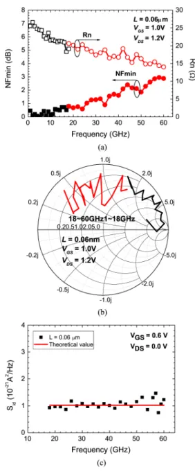
The devices used in this paper were fabricated by UMC 65-nm technology process and laid out in multifingers and multigroups structure with two sided gate access. The number of fingers and groups are eight and four, respectively, and finger length is 4 m, which might not be optimized for millimeter-wave applications. The scattering and noise parameters (minimum noise figure , equivalent noise resistance , magnitude of optimum source reflection coeffi-cient , and phase of optimum source reflection coefficient ) from 18 to 60 GHz were measured using Auriga noise and scattering parameter measurement system, and the dummy OPENandSHORTde-embedding technique was used to eliminate the parasitic contributions from the probing pads and metal in-terconnections [7]. The Auriga system was carefully calibrated and the accuracy of measurement results were confirmed by the widely used 18-GHz ATN noise and scattering parameter measurement system, as shown in Fig. 1. The good agreement between the extracted channel noise and its theoretical value for a cold device shown in Fig. 1(c) also validates measurement reliability.
The equivalent circuit shown in Fig. 2 was used to charac-terize devices’ noise behaviors, and its small-signal model ele-ments were carefully extracted using the approach presented in [8]. In this figure, the input resistance and phase delay are essential in describing the intrinsic small-signal behaviors when operating frequencies approach cutoff frequency , and the junction capacitance along with substrate resistance are used to model the RF substrate loss. In addition, the series inductances ( , , and ) are pronounced for the high-fre-quency operation. Therefore, these elements must be considered 0018-9480/$26.00 © 2010 IEEE
Fig. 1. Broadband (1–60 GHz) noise parameters. (a)NF andR versus frequency plot. (b)0 in a Smith chart. The data below 18 GHz were measured by an ATN system, while above were measured by an Auriga system. (c) Good agreement between extracted channel noise and its theoretical value for a cold device.
Fig. 2. RF noise equivalent circuit for bulk MOSFETs.
when it comes to millimeter-wave characterization and mod-eling. Table I shows the intrinsic small-signal parameters that
Fig. 3. Extracted: (a)S , (b) S , and (c) S versus frequency. The solid lines show the frequency dependence.
can benefit the characterization of the noise parameters. Be-sides, since the gate current is about or smaller than 1 nA, its associated incremental resistance 100 M and shot noise
Fig. 4. Short-circuited current(jH j) gain, unilateral power gain (U), and associated gain(G ) versus frequency.
III. CHANNELNOISESOURCECHARACTERIZATION ANDMODELING
Fig. 3 shows the extracted power spectral density (PSD) for channel noise , induced gate noise , and imaginary part of cross correlation component (denoted as , , and , respectively). To obtain these intrinsic PSDs, the noise contri-butions from the parasitic series and substrate components were eliminated following the approach presented in [9]. is shown to be frequency independent, and and to be propor-tional to and , respectively. These relations agree with the van der Ziel model [10]. Besides, our extracted results coincide with the previous findings that with the channel length scaling, are expected to increase, while and are expected to decrease [9], [11] due to the smaller oxide capacitance cou-pling [12]. Note that due to the smaller power gain, and hence, the larger inaccuracy in noise measurement, the upper measure-ment frequency is limited to 40 GHz for the m device. The short-circuit current gain , unilateral power gain , and associated gain versus frequency are also shown in Fig. 4 for the reader’s reference.
Traditionally, can be expressed as [10], [12]
(1) where J/K is the Boltzmann constant, is the ambient temperature in kelvin, is the channel con-ductance at zero drain–source voltage, and is the noise factor. The extracted noise factor versus channel length is depicted in Fig. 5, which shows that continues to increase with decreasing channel length.
Asgaran et al. [13] have developed an analytical expression for based on the classical thermal noise theory with taking the channel length modulation into account
(2) where is the drain saturation voltage at which the car-riers start to travel with their saturation velocity, is the gate
Fig. 5. Noise factor versus gate length.
Fig. 6. Extracted channel noises (symbols) and their theoretical values (lines) calculated using (2) versus drain current.
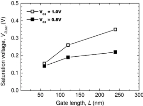
Fig. 7. Saturation voltage versus channel length.
overdrive voltage, and is the bulk charge coefficient. The ap-proximation is especially valid for shorter devices with smaller
. The extracted and modeled versus drain current for different channel sizes are shown in Fig. 6. In our experi-ments, the values for under a given gate bias were extracted by linear extrapolation in the output resistance versus drain bias plot [14], and the extraction results are also shown in Fig. 7.
According to this model [13], devices with smaller , which means more channel length modulation in the channel, would exhibit larger channel noise. As shown in Fig. 7, since continuously decreases with downscaling channel length, one can expect that would continue to increase, as shown in Fig. 6. Since (2) was a purely thermal noise based
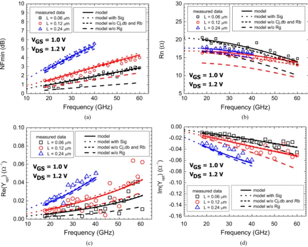
Fig. 8. Modeled: (a)NF , (b)R , (c) G , and (d)B versus frequency. The impact ofS , gate resistance, and substrate resistance on these noise param-eters are also shown in this figure.
model, the good channel noise modeling results also imply that the shot noise is not significant at 65-nm technology node, which agrees with the results shown in [15]. This also explains the increase of noise factor with the downscaling of the channel length.
IV. NOISEPARAMETERCHARACTERIZATION ANDMODELING Based on the equivalent circuit shown in Fig. 2, and the channel noises extracted in Section III, the noise parameters were simulated using Agilent Technologies’ Advanced Design System (ADS). Note that the noise sources associated with series resistances ( , , and ) and substrate resistance are considered as thermal noise, and their PSDs can be expressed as , where is the resistance value. In addi-tion, for simplificaaddi-tion, we have neglected and , as in [16]. To validate the assumption for millimeter-wave modeling, both the modeling results with and without considering are shown in Fig. 8 for comparison. This figure shows that without considering , the errors are still within acceptable range, especially for and m devices, and this supports the approximation we used in the millimeter-wave modeling. Besides, since the m device is not suitable for millimeter-wave application due to its low cutoff frequency and maximum oscillation frequency , as implied in Fig. 4, the larger errors in and for this device may not be a concern for millimeter-wave applications.
A. Intrinsic Noise Parameters
Neglecting and , the intrinsic noise parameters can be expressed as follows:
(3)
(4)
(5)
(6)
where subscript denotes the intrinsic part and K is the reference temperature.
A good figure of merit (FOM) to judge the intrinsic noise performance is . According to (3), lower can lead to smaller , which can benefit the input matching for circuit design. Fig. 9 depicts and
Fig. 9. S and R versusg .
versus for different channel lengths. It shows that with length scaling down, the increase of the channel noise tends to over-whelm the increase of , and in turn, degrades .
B. Impact of Gate Resistance on Noise Parameters
It has been shown that the gate resistance has a significant impact on the noise parameters and cannot be ignored in deep-submicrometer noise modeling [16], [17]. In fact, as the gate resistance exists, the total expressions for noise parameters have the following relations to the intrinsic ones:
(7) (8)
(9) (10) These equations suggest that the gate resistance would highly increase equivalent thermal resistance and minimum noise figure. In addition, since the gate resistance is significant in shorter devices, as shown in Fig. 10, its impact on their noise parameters is expected to be more serious. This is also confirmed in Fig. 8, where a larger error can occur in the shorter device without considering the gate resistance.
Note that for cases where is comparable or even larger than , as in [16], more accurate equations can be obtained by replacing with in (7)–(10). Besides, the value of can be changed as the used gate materials, number of gate fingers, and gate layout dependency. Therefore, the effect of on the noise parameters can be varied at different cases.
C. Impact of Substrate Resistance on Noise Parameters
Reference [18] has considered the effect of substrate resis-tance on high-frequency noise modeling. The modeling re-sults without considering the substrate resistance are also shown in Fig. 8. This figure shows, however, as compared to , the substrate resistance has a much smaller influence on noise parameters. To explain this, one can find that at very high fre-quency, the drain-side noise current’s PSD can be approximated
Fig. 10. Extracted gate resistance(R ) versus channel length.
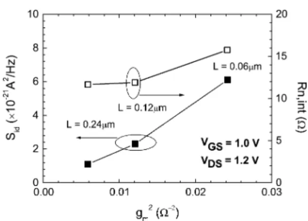
Fig. 11. R and S =S versus gate length.
by , where is the noise current PSD for the substrate resistance. As shown in Fig. 11, based on the extracted values of , is about 1/10 of at the very high frequency and can be ignored. That is, in millimeter-wave fre-quencies, the overall noise performance would be mainly dom-inated by and .
V. CONCLUSIONS
We have demonstrated the millimeter-wave noise character-ization and modeling for 65-nm MOSFETs based on the tuner method for the first time. Our experimental results show that with the continuous down scaling of channel length, the channel noise would remain the dominant noise source in the in-trinsic part of the device, and can be predicted by the traditional thermal noise theory. The sharply increased also degrades
.
Finally, the millimeter-wave noise modeling is achieved. With the help of circuit simulation, the impact of and on the noise parameters has been examined. Compared to ,
is shown to have a more serious influence on the noise parameters, and needs to be included in the millimeter-wave noise modeling.
ACKNOWLEDGMENT
The authors would like to thank the United Microelectronics Corporation (UMC), Hsinchu, Taiwan, for providing the de-vices used in this study. The authors would also like to thank Dr. D. Wandrei, Auriga Microwave, Lowell, MA, for his tech-nical support.
to extract noise parameters of 65 nm CMOS aiming 70–90 GHz ap-plications,” in IEEE Radio Freq. Integr. Circuits Symp., Jun. 2009, pp. 397–400.
[6] K. H. K. Yau, M. Khanpour, M.-T Yang, P. Schvan, and S. P. Voinigescu, “On-die source-pull for the characterization of the W -band noise performance of 65 nm general purpose (GP) and low power (LP) n-MOSFETs,” in IEEE MTT-S Int. Microw. Symp. Dig., Jun. 2009, pp. 773–776.
[7] G. Knoblinger, “RF-noise of deep-submicron MOSFETs: Extraction and modeling,” in Proc. Eur. Solid-State Device Res. Conf., 2001, pp. 331–334.
[8] S. C. Wang, G. W. Huang, K. M. Chen, A. S. Peng, H. C. Tseng, and T. L. Hsu, “A practical method to extract extrinsic parameters for the sil-icon MOSFET small signal model,” in Proc. NSTI Nanotechnol. Conf., Boston, MA, 2004, pp. 151–154.
[9] C. H. Chen, M. J. Deen, Y. Cheng, and M. Matloubian, “Extraction of the induced gate noise, channel noise and their correlation in sub-mi-cron MOSFET’s from RF noise measurements,” IEEE Trans. Electron Devices, vol. 48, no. 12, pp. 2884–2892, Dec. 2001.
[10] A. van der Ziel, Noise in Solid State Devices and Circuits. New York: Wiley, 1986.
[11] A. J. Scholten, L. F. Tiemeijer, R. Langevelde, R. J. Havens, A. T. A. Z. van Duijnhoven, and V. C. Venezia, “Noise modeling for RF CMOS circuit simulations,” IEEE Trans. Electron. Devices, vol. 50, no. 3, pp. 618–632, Mar. 2003.
[12] A. F. Tong, W. M. Lim, K. S. Yeo, C. B. Sia, and W. C. Zhou, “A scalable RF CMOS noise model,” IEEE Trans. Microw. Theory Tech., vol. 57, no. 5, pp. 1009–1019, May 2009.
[13] S. Asgaran, M. J. Deen, and C.-H. Chen, “Analytical modeling of MOSFET’s channel noise and noise parameters,” IEEE Trans. Elec-tron Devices, vol. 51, no. 12, pp. 2109–2114, Dec. 2004.
[14] J. J.-Y. Kuo, W. P.-N. Chen, and P. Su, “Investigation of analogue per-formance for process-induced-strained PMOSFETs,” Semicond. Sci. Technol., vol. 22, pp. 404–407, 2007.
[15] J. Jeon, J. Lee, J. Kim, C. H. Park, H. Lee, H. Oh, H.-K. Kang, B.-G. Park, and H. Shin, “The first observation of shot noise characteristics in 10-nm scale MOSFETs,” in VLSI Technol. Symp., 2009, pp. 48–49. [16] J. Jeon, I. Song, I. M. Kang, Y. Yun, B.-G. Paark, J. D. Lee, and H. Shin, “A new noise parameter model of short-channel MOSFETs,” in IEEE Radio Freq. Integr. Circuits Symp., Jun. 2007, pp. 639–642. [17] M. J. Deen, C. H. Chen, S. Asgaran, G. A. Rezvani, J. Tao, and Y.
Kiyota, “High-frequency noise of modern MOSFETs: Compact mod-eling and measurement issues,” IEEE Trans. Electron Devices, vol. 53, no. 9, pp. 2062–2081, Sep. 2006.
[18] C. Enz, “An MOS transistor model for RFIC design valid in all regions of operation,” IEEE Trans. Microw. Theory Tech., vol. 50, no. 1, pp. 342–359, Jan. 2002.
Sheng-Chun Wang received the B.S. and M.S.
degrees in electrical engineering from National Cheng Kung University, Tainan, Taiwan, in 1999 and 2001, respectively, and is currently working toward the Ph.D. degree at Chiao Tung University, Hsinchu, Taiwan.
In 2001, he joined the National Nano Device Laboratories, Hsinchu, Taiwan, as an Assistant Researcher. His current research interests focus on small-signal and noise characterization and modeling for RF CMOS devices.
for advanced CMOS devices, and device/circuit interactions in nano-CMOS. He has authored or coauthored over 90 research papers in refereed journals and international conference proceedings.
Kun-Ming Chen received the M.S. degree and Ph.D.
degree in electronics engineering from National Chiao Tung University, Hsinchu, Taiwan, in 1996 and 2000, respectively.
In 2000, he joined the National Nano Device Laboratories, Hsinchu, Taiwan, as an Associate Researcher, and in 2007 became a Researcher. He has been engaged in research on the microwave device process and characterization.
Kuo-Hsiang Liao received the M.S. degree in
elec-tronic engineering from the National Changhua Uni-versity of Education, Taiwan, Taiwan, in 2005.
In 2005, he joined the National Nano Device Laboratories, Hsinchu, Taiwan, as an Assistant Researcher. He has been engaged in research on RF device characterization and modeling.
Bo-Yuan Chen was born in Miaoli, Taiwan, in 1980.
He received the M.S. degree in materials science and engineering from National Dong Hwa University, Hualien, Taiwan, in 2006.
In 2006, he joined National Nano Device Labora-tories, Hsinchu, Taiwan, as an Assistant Researcher. He has been engaged in research on III–V compound semiconductors and RF device characterization.
Sheng-Yi Huang received the B.S. degree in
electrical engineering from National Cheng Kung University, Tainan, Taiwan, in 2001, and the M.S. and Ph.D. degrees in electronics engineering from National Chiao Tung University Hsinchu, Taiwan, in 2003 and 2007, respectively.
Since 2003, he has been with the Advanced Technology Development Division, United Micro-electronics Corporation (UMC), Hsinchu, Taiwan, where he is involved with RF-related technolo-gies. His current research focuses on advanced mixed-mode and RF CMOS design including device modeling, noise charac-terization, power behavior, and reliability studies.
Cheng-Choug Hung received the B.S. and M.S.E.E.
degrees in electrical engineering from National Cheng Kung University, Tainan, Taiwan, in 1996 and 1999, respectively.
He is currently with the Advanced Technology Department, United Microelectronics Corporation (UMC), Hsinchu, Taiwan, as an RF Device Devel-opment Manager. His current responsibility and research focuses on RF CMOS technology char-acterization/delivery including active and passive devices.
Guo-Wei Huang (S’94–M’97) was born in Taipei,
Taiwan, in 1969. He received the B.S. degree and Ph.D. degree in electronics engineering from Na-tional Chiao Tung University, Hsinchu, Taiwan, in 1991 and 1997, respectively.
In 1997, he joined National Nano Device Labo-ratories (NDL), Hsinchu, Taiwan, where he is cur-rently a Researcher and Manager of the High-Fre-quency Technology Division. Since August 2008, he has been an Adjunct Associate Professor with the De-partment of Electronics Engineering, National Chiao Tung University. His current research interests focus on characterization and modeling techniques of high-frequency devices, and characterization and veri-fication of RF integrated circuits (RFICs)/monolithic microwave integrated cir-cuits (MMICs).