Properties and thermal stability of chemically vapor deposited W-rich WSi x thin films
M. T. Wang, Y. C. Lin, M. S. Chuang, M. C. Chun, L. J. Chen, and M. C. Chen
Citation: Journal of Vacuum Science & Technology B 17, 385 (1999); doi: 10.1116/1.590567 View online: http://dx.doi.org/10.1116/1.590567
View Table of Contents: http://scitation.aip.org/content/avs/journal/jvstb/17/2?ver=pdfcov
Published by the AVS: Science & Technology of Materials, Interfaces, and Processing
Articles you may be interested in
Thermal stability of chemical vapor deposition grown W and W N x thin films in low- k integration structure
J. Vac. Sci. Technol. B 24, 1428 (2006); 10.1116/1.2203638
Effect of NH 3 thermal treatment on an atomic layer deposited on tungsten films and formation of W–B–N
J. Vac. Sci. Technol. B 21, 1466 (2003); 10.1116/1.1585064
Atomic-layer-deposited WN x C y thin films as diffusion barrier for copper metallization
Appl. Phys. Lett. 82, 4486 (2003); 10.1063/1.1585111
Effects of composition and N 2 plasma treatment on the barrier effectiveness of chemically vapor deposited WSi x films
J. Vac. Sci. Technol. B 18, 1929 (2000); 10.1116/1.1305273
Thermal stability of selective chemical vapor deposited tungsten contact and effects of in situ N 2 plasma treatment
M. C. Chun
National Nano Device Laboratory, 1001 Ta Hsueh Rd., Hsinchu, Taiwan L. J. Chen
Department of Submicron Technology Development, ERSO/ITRI, Hsinchu, Taiwan M. C. Chena)
Department of Electronics Engineering, National Chiao-Tung University, Hsinchu, Taiwan ~Received 27 February 1998; accepted 18 December 1998!
The tungsten-rich~Si/W atomic ratio less than 2.0! chemical vapor deposition ~CVD!-WSix layer
was found to be an efficient diffusion barrier against Cu diffusion. In this study, the properties and thermal stability of the W-rich WSix films chemically vapor deposited at various deposition
temperatures, pressures, and SiH4/WF6 reactant gas flow ratios were investigated. With SiH4/WF6 flow rates of 6/2 sccm and a total gas pressure of 12 mTorr, the activation energy of the CVD process was determined to be 3.0 kcal/mole, and the film deposited at 250 °C has a Si/W atomic ratio of unity. The WSixfilms have a low residual stress, low electrical resistivity, and excellent step
coverage. For the WSix layers deposited on Si substrates, the residual stress varies from 7 to 9
3108dynes/cm2depending on the deposition temperature. The resistivity of the WSi
xfilms varies
from 200 to 340 mV cm; higher deposition temperatures and SiH4/WF6 flow ratios resulted in higher film resistivities. The as-deposited amorphous WSix layer is thermally stable up to 600 °C;
however, crystallization of the deposited film takes place at 650 °C and WSixwas transformed into
WSi2 phase when the WSix/Si structure was thermally annealed at temperatures above 650 °C.
© 1999 American Vacuum Society.@S0734-211X~99!03602-1#
I. INTRODUCTION
It was found recently that a tungsten-rich ~Si/W atomic ratio less than 2.0! chemical vapor deposition ~CVD!-WSix layer served efficiently as diffusion barrier against Cu diffusion.1,2 The thermal stability of Cu/WSix~50 nm!/p1-n
junction diodes was found to reach 500 °C; with an in situ N2 plasma treatment on the surface of WSixlayers, the resultant
Cu/WSiN/WSix~50 nm!/p1-n junction diodes were able to
retain integrity of their electrical characteristics up to at least 600 °C.2Moreover, the tungsten-rich CVD-WSixfilms were
found to have a low residual stress, low electrical resistivity, and excellent step coverage. This indicates that the tungsten-rich CVD-WSix films possess great potential in application
to Cu metallization system. Thus, a systemic study of tungsten-rich CVD-WSixfilms is vital to their applications in
ultralarge scale integration~ULSI! circuits.
Refractory metal silicides have been intensively studied for potential use as interconnection in ULSI circuits.3,4These materials offer good thermal stability and good electrical conductivity. Among them, tungsten silicide ~WSix) is one
of the most promising materials because of its good compat-ibility with conventional ULSI fabrication processes.5–21 Sputter deposited WSixfilms have been widely used in
inte-grated circuits ~ICs! manufacture.4,6 In general, the sputter deposited WSix used in ICs manufacture has a Si/W atomic
ratio larger than 2.0, and is often referred to as ‘‘silicon-rich WSix.’’ The as-sputtered WSix films have a resistivity of
600–900 mV cm, which decreases to about 50mV cm after annealing at 1000 °C.6 However, it is difficult to deposit WSixfilms, with acceptable step coverage, into contact holes
of deep subhalf micron dimensions using physical vapor deposition ~PVD! method. In contrast, CVD method gener-ally offers superior step coverage of conformal deposition; thus chemically vapor deposited WSix~CVD-WSix) layer is
becoming very attractive in ULSI application.5
The first systemic study of CVD-WSix, to our
knowl-edge, was done by Brors et al.,7 they proposed to deposit WSixfilms in a cold wall reactor using SiH4/WF6as reactive gas mixtures and obtained a good quality silicide films with a resistivity as low as 30 mV cm after a postdeposition an-nealing treatment. It was reported that the residual stress in CVD-WSix films decreased linearly with increasing silicon
content in the WSixfilm.2,22In addition, it was found that the
resistivity of as-deposited CVD-WSixfilm increased with
in-creasing deposition temperature.7,13,22 Although many stud-ies have been dedicated to the propertstud-ies and thermal stabil-ity of silicon-rich ~Si/W atomic ratio larger than 2.0! nonstoichiometric CVD-WSix films, little work has been
done on the tungsten-rich CVD-WSixlayers.
In this study, the properties and thermal stability of tungsten-rich nonstoichiometric CVD-WSix thin films were
systemically investigated. The WSixthin layers were
depos-*No proof corrections received from author prior to publication. a!Electronic mail: [email protected]
ited by low pressure chemical vapor deposition ~LPCVD! method using the SiH4reduction of WF6. The properties of CVD-WSix layers including crystalline phase, deposition
rate, electrical resistivity, residual stress, surface roughness, and step coverage were investigated. The thermal stability of CVD-WSixlayers was also investigated using various
tech-niques @scanning electron microscopy ~SEM!, x-ray diffrac-tion ~XRD! analyses, Rutherford backscattering spectros-copy~RBS!, and sheet resistance measurements#. The results of this study might be useful in multilevel metallization for ULSI circuits.
II. EXPERIMENT
The test samples were fabricated on n type, ~100!-oriented, 4-in.-diam silicon wafers with 4–7 V cm nominal resistivity. After RCA standard cleaning, one group of wa-fers was thermally oxidized to grow a 500-nm-thick SiO2 layer. Unpatterned samples of WSix/Si and WSix/SiO2/Si structures were then prepared for material analysis. For step coverage study, patterned samples with trenches having as-pect ratios ranging from 1 to 4 were also prepared.
The WSix layers were deposited by CVD method using
SiH4 reduction of WF6. Prior to the WSix deposition, both
the bare Si and SiO2/Si wafers were dipped in dilute HF
~50:1! for 30 s, followed by a rinse in DI water for 3 min and spin dry. The wafers were then loaded into a load-locked cold wall CVD system within 5 min and transferred by a robot arm to the deposition chamber without exposure to the atmosphere. The base pressure of the CVD chamber was 1026 Torr. In this study, WSix films were chemically vapor
deposited from SiH4/WF6 gas mixtures with the conditions illustrated as follows: substrate temperature 150– 450 °C, to-tal gas pressure 12–20 mTorr, WF6 flow rate 2 sccm, and SiH4flow rate 4–100 sccm.
The properties of the CVD-WSixlayers including
crystal-line phase, deposition rate, electrical resistivity, residual stress, surface roughness, and step coverage were investi-gated. The samples of the WSix/Si and WSix/SiO2/Si struc-tures were thermally annealed in N2flowing furnace for 30
min at a temperature ranging from 400 to 800 °C. The varia-tion of sheet resistance with respect to the annealing tem-perature was used to monitor the thermal stability. Atomic force microscopy ~AFM! was employed to characterize the surface roughness. XRD analysis was used for phase identi-fication. RBS was used to determine the Si/W atomic ratio of WSixfilms and to examine the interdiffusion between W and
Si substrate at the WSix/Si interface. Moreover, SEM was
employed to measure the film thickness and observe the sur-face morphology as well as the change of microstructure.
III. RESULTS AND DISCUSSION A. Properties of CVD-WSix thin films
1. Effects of SiH4/WF6 flow rate
Three different types of film microstructure, a-W phase,
b-W phase, and amorphous WSix phase, were obtained by the SiH4 reduction of WF6 with different SiH4/WF6 flow ratio, as revealed by XRD analysis ~Fig. 1!. At a substrate temperature of 300 °C and with a total gas pressure of 20 mTorr,a-W diffraction peaks were detected for films depos-ited with SiH4/WF6 flow ratio lower than 1.0 @Fig. 1~a!#, while b-W peaks were detected for films deposited with SiH4/WF6flow ratio ranging from 1.0 to 1.5@Fig. 1~b!#. With the SiH4/WF6flow ratio higher than 2, the structure of WSix
films was eventually amorphous@Fig. 1~c!#.
To investigate the effects of SiH4/WF6 flow ratio on the resistivity and Si/W atomic ratio of WSix films, the CVD
FIG. 1. XRD spectra of WSix films deposited on bare Si substrate with
SiH4/WF6flow ratio of~a! 0.25, ~b! 1.5, and ~c! 3.0. The films were depos-ited at 300 °C with a total gas pressure of 20 mTorr.
FIG. 2. Resistivity of WSixfilms vs SiH4/WF6flow ratio. The WSixfilms
were deposited at 250 °C with a total gas pressure of 12 mTorr and WF6 flow rate of 2 sccm.
FIG. 3. Deposition rate of WSixfilms vs deposition temperature. The WSix
films were deposited with a total gas pressure of 12 mTorr and SiH4/WF6 flow rates of 6/2 sccm.
386 Wanget al.: Properties and thermal stability of CVD WSixthin films 386
process was conducted at a substrate temperature of 250 °C and with a SiH4flow rate ranging from 4 to 100 sccm, while keeping the WF6flow rate at 2 sccm and the total gas pres-sure at 12 mTorr. Figure 2 shows the resistivity of CVD-WSix films versus SiH4/WF6 flow ratio. The resistivity of WSix layers increases with increasing flow ratio of
SiH4/WF6; this increase in resistivity is presumably related to an increased amount of Si incorporated in the WSixlayer.
We found that the Si/W atomic ratio in the WSix layer
in-creased from 1.0 to 1.3 as the SiH4/WF6flow ratio was in-creased from 3 to 50, as determined by RBS measurements. Similar results were reported by Clark, although the SiH4/WF6flow ratio ranged from 85 to 315, deposition tem-perature ranged from 330 to 360 °C and the resultant WSix
layer was nonstoichiometric silicon-rich (x.2) in his study.22
2. Deposition temperature effect
The CVD of WSix films was conducted at temperatures
ranging from 150 to 450 °C with a total gas pressure of 12 mTorr, WF6 flow rate of 2 sccm, and SiH4 flow rate of 6 sccm. Figures 3 and 4 show the deposition rate and resistiv-ity of WSix films versus deposition temperature. Below
300 °C, the surface reaction might be the rate limiting pro-cess, and the activation energy of the CVD process was de-termined to be 3.0 kcal/mole. At temperatures above 300 °C, the deposition rate was independent of the substrate tempera-ture; as a result, the process was possibly controlled by mass
transfer mechanism. Thermodynamically, silane is an un-stable compound and will decompose into silicon and hydro-gen. Since the decomposition of SiH4is a thermally activated process, the amount of Si incorporated into WSix films will
increase with increasing deposition temperature. It was re-ported that the resistivity of chemically vapor deposited amorphous WSix films increased with increasing Si content
in the as-deposited films.20,22 The reported observation is thus consistent with the results of this work that the increase in deposition temperature resulted in an increase in resistiv-ity for the as-deposited WSix films.
FIG. 5. Residual stress in as-deposited WSixfilms as a function of deposition
temperature. The WSixfilms were deposited at a total gas pressure of 12
mTorr and SiH4/WF6flow rates of 6/2 sccm.
FIG. 6. Surface roughness of as-deposited CVD-WSixfilms vs deposition
temperature. The WSixfilms were deposited at a total gas pressure of 12
mTorr and SiH4/WF6flow rates of 6/2 sccm.
FIG. 7. AFM micrographs for WSixfilms deposited at substrate temperature
of~a! 250 and ~b! 450 °C. FIG. 4. Resistivity of WSixfilms vs deposition temperature. The WSixfilms
were deposited at a total gas pressure of 12 mTorr and SiH4/WF6flow rates of 6/2 sccm.
3. Residual stress
The residual stress was measured using a Tencor’s FLX-2320 system. The value of stress was determined according to Eq.~1!, s56~12E n! t 2 d
F
1 R2 1 R0G
, ~1!wheres is the stress, E is the Young’s modulus of Si sub-strate,n is the Poisson ratio of Si substrate, t is the thickness of WSixfilm, d is the thickness of Si substrate, while R0and
R are the radii of curvature of the substrate before and after
the film deposition, respectively.
Figure 5 shows the residual stress in as-deposited WSix
films versus deposition temperature. The stress decreases slightly with increasing deposition temperature. This is pre-sumably due to larger amount of Si incorporated in the WSix
layer at higher deposition temperatures. This result agrees with the reported work in literature that the stress of WSixis
influenced by the Si/W atomic ratio in the WSix film.
22,23 It should be noted that a good adherence can be obtained for the CVD-WSix layer deposited on Si substrate at
tem-peratures higher than 200 °C. Peeling of WSix layer on Si
substrate was found for the WSix layer deposited at 150 °C
to a thickness of 220 nm. Moreover, peeling of WSix layer
on SiO2was found for the WSix layer deposited at 200 °C.
4. Surface roughness
The surface roughness of CVD-WSixfilms was measured
using AFM on unpatterned WSix/Si samples. Figure 6 shows
the surface roughness versus deposition temperature for as-deposited CVD-WSix layers. A fairly smooth surface was obtained for the WSix films deposited at temperatures be-tween 250 and 400 °C, as analyzed using AFM @Fig. 7~a!#. However, the surface roughness increased drastically for the films deposited at temperatures above 450 °C @Fig. 7~b!#. Particles generated by gas phase nucleation might lead to the surface roughness. It has been reported that the gas phase nucleation occurred at temperatures above 400 °C and with SiH4/WF6 flow ratio higher than unity. Moreover, it was found that the particle generation rate increased with increas-ing deposition pressure.24
5. Step coverage
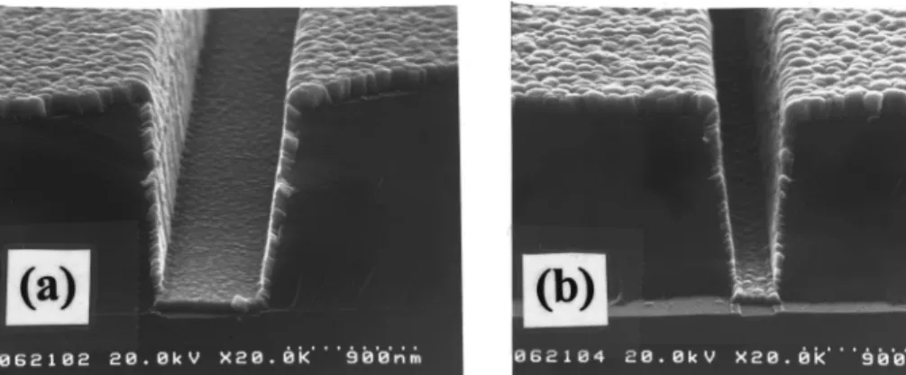
A highly conformal deposition of CVD-WSix films was
obtained. Figure 8 shows the WSix films deposited on
sub-micron trenches with aspect ratios of 2 and 4 using the depo-sition condition illustrated as follows: substrate temperature 250 °C, total gas pressure 12 mTorr, WF6flow rate 2 sccm, and SiH4flow rate 6 sccm. We referred to this condition as ‘‘standard deposition condition’’ hereafter.
FIG. 9. XRD spectra for as-deposited and thermally annealed WSix~220
nm!/Si samples.
FIG. 10. XRD spectra for as-deposited and thermally annealed WSix~50
nm!/SiO2/Si samples.
FIG. 8. Step coverage of WSix films
deposited on submicron trenches with aspect ratio of~a! 2.0 and ~b! 4.0.
388 Wanget al.: Properties and thermal stability of CVD WSixthin films 388
B. Thermal stability of CVD-WSixfilms
The thermal stability of the WSix layers, deposited using the standard deposition condition on bare Si and SiO2/Si sub-strates to produce WSix~220 nm!/Si and WSix~50 nm!/ SiO2/Si structures, respectively, was investigated using the techniques of XRD, RBS, SEM, and the sheet resistance measurement.
1. XRD analyses
For WSix~220 nm!/Si samples, the as-deposited WSix films are amorphous, as indicated by XRD analysis shown in Fig. 9. A broad peak was present clearly at 2u angle of 39°– 43°. Since at least six diffraction peaks available to various phases ~110-a-W, 330-W5Si3, 202-W5Si3, 420-W5Si3, 411-W5Si3, and 110-WSi2) are located within this 2u range, it is not possible to draw any conclusion from the
position of this broad peak. After annealing at 600 °C, the WSixlayer retained its original amorphous phase. However,
a number of diffraction peaks belonging to WSi2 phase ap-peared after the sample was annealed at 650 °C. The pres-ence of WSi2 phase indicates that reaction occurred at the WSix/Si interface.
XRD spectra for as-deposited and thermally annealed WSix~50 nm!/SiO2/Si samples are illustrated in Fig. 10. After annealing at 650 °C, a very weak peak of W5Si3 phase ap-peared at 2u angle of about 37°, and the intensity of the W5Si3 peaks increased with increasing annealing tempera-ture. However, no peak of WSi2 phase was observed even after annealing at 800 °C. This different behavior between the WSix/Si and WSix/SiO2/Si structures is apparently re-lated to the presence of SiO2layer in the latter structure. The SiO2layer prevented out diffusion of Si atoms from the
sub-FIG. 11. Sheet resistance change vs annealing temperature for WSix/Si and
WSix/SiO2/Si samples.
FIG. 12. Thickness change of WSix layer vs annealing temperature for
WSix/Si and WSix/SiO2/Si samples.
FIG. 13. Cross-sectional SEM micro-graphs for WSix/Si samples ~a!
as-deposited, and thermally annealed at
strate to the WSixlayer; thus, the Si deficient WSixlayer was
not able to form stable WSi2phase during thermal annealing. Moreover, since no signal of WSi2 phase was observed for the thermally annealed WSix/SiO2/Si sample, we excluded the possibility that the as-deposited WSix film contained
amorphous WSi2. Therefore, we conclude that the as-deposited WSix is a mixture of amorphous phase of W and
Si, together with possible existence of amorphous phase of W5Si3.6
2. Sheet resistance measurements
The sheet resistance change of annealed samples, normal-ized to the as-deposited sheet resistance value, is denoted as DRs/Rs ~%! and defined as follows:
DRs Rs ~%!5
F
Rsafter anneal2Rsas-deposited
Rsas-deposited
G
3100%. ~2!
Figure 11 shows the sheet resistance change versus an-nealing temperature for the WSix/Si and WSix/SiO2/Si samples, in which the WSix layers were deposited using the
standard deposition condition. The sheet resistance of WSix/Si remained constant up to 600 °C, implying that the
amorphous structure of WSix film remained unchanged, as
confirmed by XRD patterns shown in Fig. 9. With the samples annealed at temperatures above 650 °C, the sheet resistance decreased rapidly with increasing annealing tem-perature. This is attributed to the formation of the low resis-tivity WSi2phase at temperatures above 650 °C~Fig. 9!. For WSix~50 nm!/SiO2/Si samples, the sheet resistance also showed decreasing trend after annealing at temperatures above 650 °C; however, the extent of decrease is much smaller than the WSix/Si samples. The decrease in sheet
re-sistance was presumably due to crystallization and grain growth of W5Si3phase~Fig. 10!.
3. Thickness change of WSix layers
The thermal annealing was found to result in the thickness change of WSix layers for WSix/Si samples. The thickness change normalized to the as-deposited thickness is denoted as Dt/t ~%! and defined as follows:
Dt t ~%!5
F
tafter anneal2tas-deposited
tas-deposited
G
3100%, ~3!
where t is the thickness of WSix layers.
FIG. 14. Rutherford backscattering spectra for WSix/Si samples~a! as-deposited, and thermally annealed at ~b! 600, ~c! 650, and ~d! 700 °C.
390 Wanget al.: Properties and thermal stability of CVD WSixthin films 390
peratures up to 600 °C; however, the thickness made a sig-nificant increase at temperatures above 600 °C and the nor-malized increase finally reached a saturated value of about 50% when the sample was annealed at temperatures above 700 °C. This is consistent with the results of XRD analysis ~Fig. 9! and sheet resistance measurements ~Fig. 11! that WSi2 phase was formed at temperatures above 600 °C. For WSix/SiO2/Si samples, the thickness of WSixlayers showed
no obvious change after thermal annealing at temperatures up to 800 °C. Figure 13 shows the cross sectional SEM mi-crographs for WSix/Si samples before and after thermal
an-nealing. The increase in thickness of WSixlayers was clearly
observed for WSix/Si samples annealed at temperatures
above 650 °C. Moreover, the amorphous phase of the as-deposited WSixlayer became a grain-like structure,
presum-ably related to the WSi2 grains.
4. RBS analyses
The observed spectra from 2.0 MeV He1RBS measure-ments for the as-deposited and thermally annealed WSix/Si
samples are illustrated in Fig. 14. The as-deposited sample exhibits one RBS peak of channeling energies relating to W in the WSix layer, and two edges which relate to,
respec-tively, the Si in the WSixlayer~at about 1.12 MeV! and the
Si substrate~at about 0.88 MeV! @Fig. 14~a!#. After anneal-ing at 600 °C, no obvious change in the RBS spectrum was observed@Fig. 14~b!#. The Si/W atomic ratio of as-deposited WSix layers was determined to be 1.0 and remained
un-changed after annealing at 600 °C. This suggests that the WSix/Si structure remained stable up to at least 600 °C.
Af-ter annealing at 650 °C, the width of the W peak increased, indicating an increase in thickness of the W containing layer @Fig. 14~c!#. Upon annealing at 700 °C, the width of the W peak increased to about 1.5 times the original width @Fig. 14~d!#. This is consistent with our previous results of the increase in the WSix thickness shown in Fig. 12. The Si/W atomic ratio was determined to be 66/34 and a small increase in Si peak intensity at backing energy of 1.12 MeV was also observed, indicating the increase of Si/W atomic ratio for the WSixlayer. This clearly indicates the transformation of WSix
into WSi2phase.
IV. SUMMARY
The properties and thermal stability of W-rich CVD-WSix
thin films were investigated. We found that the WSix layers
have a low stress, low electrical resistivity, and excellent step coverage. For WSix layers deposited on Si substrates, the
stress varies from 7 to 93108 dynes/cm2 depending on the deposition temperature. The resistivity of the WSixfilms
var-ies from 200 to 340mV cm; higher deposition temperatures
posited at a temperature of 250 °C has a Si/W atomic ratio of unity. As for the thermal stability of CVD-WSix films, we
found that the WSix/Si contact system is thermally stable up
to at least 600 °C. However, WSix was transformed into
WSi2 phase when the WSix/Si structure was thermally
an-nealed at temperatures above 650 °C.
ACKNOWLEDGMENT
This work was supported by the National Science Council ~ROC! under Contract No. NSC86-2215-E-009-040.
1M. T. Wang, Y. C. Lin, J. Y. Lee, C. C. Wang, and M. C. Chen, J. Electrochem. Soc.~to be published!.
2
M. T. Wang, Y. C. Lin, J. Y. Lee, C. C. Wang, and M. C. Chen ~unpub-lished!.
3T. P. Chow and A. J. Steckl, IEEE Trans. Electron Devices ED-30, 1480
~1983!.
4
S. P. Murarka, J. Vac. Sci. Technol. 17, 775~1980!. 5
J. E. J. Schmitz, Chemical Vapor Deposition of Tungsten and Tungsten Silicides for VLSI/ULSI Applications~Noyes, Park Ridge, NJ, 1992!, pp. 171–208.
6S. R. Wilson, C. J. Tracy, and J. L. Freeman, Jr., Handbook of Multilevel Metallization for Integrated Circuits: Materials, Technology, and Appli-cations~Noyes, Park Ridge, NJ, 1993!, pp. 53–55.
7D. L. Brors, J. A. Fair, K. A. Monnig, and K. C. Saraswat, Solid State Technol. 26, 183~1983!.
8
M. Suzuki, N. Kobayashi, and K. Mukai, Tungsten and Other Advanced Metals for VLSI/ULSI Applications V, edited by S. S. Wang and S. Fu-rukawa~Materials Research Society, Pittsburgh, PA, 1990!, pp. 259–265. 9D. L. Brors, J. A. Fair, and K. Monnig, Semiconductor International, May
1984~unpublished!, p. 82. 10
S. Sachdev and R. Castellano, Semiconductor International, May 1985
~unpublished!, p. 306.
11R. Togei, J. Appl. Phys. 59, 3582~1986!.
12M. Kottke, F. Pintchovski, T. R. White, and P. J. Tobin, J. Appl. Phys. 60, 2835~1986!.
13
Y. Shioya, T. Itoh, I. Kobayashi, and M. Maeda, J. Electrochem. Soc.
133, 1475~1986!.
14Y. Shioya and M. Maeda, J. Appl. Phys. 60, 327~1986!.
15C. Bernard, R. Madar, and Y. Pauleau, Semicond. Sci. Technol. 32, 79
~1989!.
16K. C. Saraswat, D. L. Brors, J. A. Fair, K. A. Monnig, and R. Beyers, IEEE Trans. Electron Devices ED-30, 1497~1983!.
17D. K. Sadana, A. E. Morgan, M. H. Norcott, and S. Naik, J. Appl. Phys.
62, 2830~1987!.
18
D. Dobkin, L. Bartholomew, G. McDaniel, and J. DeDontney, J. Electro-chem. Soc. 137, 1623~1990!.
19M. Suzuki, N. Kobayashi, K. Mukai, and S. Kondo, J. Electrochem. Soc.
137, 3213~1990!.
20
J. H. Sone and H. J. Kim, in Advanced Metallization and Processing for Semiconductor Devices and Circuits, edited by A. Katz, S. P. Murarka, Y. I. Nissim, and James M. E. Harper~Materials Research Society, Pitts-burgh, PA, 1990!, Vol. 260, pp. 621–626.
21N. Thomas, A. M. Dutron, C. Vahlas, C. Bernard, and R. Madar, J. Electrochem. Soc. 142, 1608~1995!.
22T. E. Clark, J. Vac. Sci. Technol. B 6, 1678~1988!.
23Y. Shioya, T. Itoh, S. Inoue, and M. Maeda, J. Appl. Phys. 58, 4194
~1985!.
24
E. J. McInerney, T. W. Mountsier, B. L. Chin, and E. K. Broadbent, J. Vac. Sci. Technol. B 11, 734~1993!.