This article was downloaded by: [National Chiao Tung University 國立交通大學] On: 27 April 2014, At: 20:04
Publisher: Taylor & Francis
Informa Ltd Registered in England and Wales Registered Number: 1072954 Registered office: Mortimer House, 37-41 Mortimer Street, London W1T 3JH, UK
Journal of the Chinese Institute of Engineers
Publication details, including instructions for authors and subscription information:
http://www.tandfonline.com/loi/tcie20
New high
‐speed low‐power current‐mode CMOS
sense amplifier
Shang‐Ming Wang a & Ching‐Yuan Wu b a
Institute of Electronics , National Chiao‐Tung University , Hsinchu, Taiwan 300, R.O.C. Phone: 886–3–5777897 Fax: 886–3–5777897 E-mail:
b Institute of Electronics , National Chiao‐Tung University , Hsinchu, Taiwan 300, R.O.C. Published online: 03 Mar 2011.
To cite this article: Shang‐Ming Wang & Ching‐Yuan Wu (2003) New high‐speed low‐power current‐mode CMOS sense amplifier, Journal of the Chinese Institute of Engineers, 26:3, 367-370, DOI: 10.1080/02533839.2003.9670789
To link to this article: http://dx.doi.org/10.1080/02533839.2003.9670789
PLEASE SCROLL DOWN FOR ARTICLE
Taylor & Francis makes every effort to ensure the accuracy of all the information (the “Content”) contained in the publications on our platform. However, Taylor & Francis, our agents, and our licensors make no
representations or warranties whatsoever as to the accuracy, completeness, or suitability for any purpose of the Content. Any opinions and views expressed in this publication are the opinions and views of the authors, and are not the views of or endorsed by Taylor & Francis. The accuracy of the Content should not be relied upon and should be independently verified with primary sources of information. Taylor and Francis shall not be liable for any losses, actions, claims, proceedings, demands, costs, expenses, damages, and other liabilities whatsoever or howsoever caused arising directly or indirectly in connection with, in relation to or arising out of the use of the Content.
This article may be used for research, teaching, and private study purposes. Any substantial or systematic reproduction, redistribution, reselling, loan, sub-licensing, systematic supply, or distribution in any
form to anyone is expressly forbidden. Terms & Conditions of access and use can be found at http:// www.tandfonline.com/page/terms-and-conditions
Short Paper
NEW HIGH-SPEED LOW-POWER CURRENT-MODE CMOS
SENSE AMPLIFIER
Shang-Ming Wang* and Ching-Yuan Wu
ABSTRACT
A novel low-power current-mode sense amplifier for fast CMOS SRAM applica-tions is presented. It is based on the current mode approach. The sensing speed is independent of the bit-line and data-line capacitances and a separated positive feed-back technique is employed to give the circuit high-speed, low-power operation. Based on the new current-mode sense amplifier, a 32Kx8 SRAM chip was designed and fabricated. The access time is 9ns at a supply voltage of 3V and the active current is 28mA at 100MHz.
Key Words: current-mode, sense amplifier, SRAM, positive feedback.
*Corresponding author. (Tel: 5777897; Fax: 886-3-5779832; E-mail: [email protected])
The authors are with the Institute of Electronics, National Chiao-Tung University, Hsinchu, Taiwan 300, R.O.C.
I. INTRODUCTION
Power dissipation has become an important de-sign criterion of VLSI chips. Several dede-sign tech-niques have been proposed to reduce the power dis-sipation of static RAM (Itoh et al., 1995) in the past. On the other hand, several current mode sensing cir-cuits (Seevinck, 1990; Seevinck et al., 1991; Blalock and Jaeger, 1991) have been proposed to overcome the problem of possible speed degradation due to large bit-line or data-line capacitances.
As the density of memory devices increases, inevitably the associated parasitic capacitances also increase. Large capacitive loads cause a major sens-ing delay in memory devices, so high speed sense amplification of small memory cell signals is the key to achieving a fast access time in SRAMs. Conven-tional sense amplifiers are based on voltage sensing techniques, which are sensitive to parasitic capa-citance. Recent approaches to designing sense am-plifiers employ current sensing techniques (Shibata, 1996; Wicht et al., 2001). The advantages in term of speed are obvious and very attractive, especially if the supply voltage is low and the memories are
large. In this paper, a novel current-mode sense amplifier, which gives fast access time and low power consumption, is presented. In addition, it is insensi-tive to both bit-line and data-line capacitances.
II. CIRCUIT DESCRIPTION
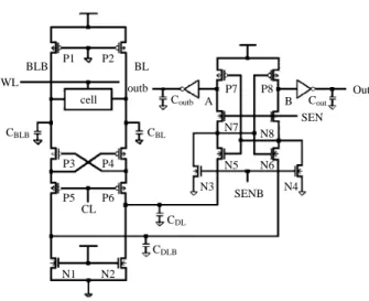
The new circuit is shown in Fig. 1. The current conveyor (P3-P6) used in the conventional current sense amplifier is adopted for column sensing. The
P1 and P2 are used to pull the bit-lines close to the
supply voltage to attain memory cell stability. The precharge equalizing device is omitted, because the current conveyor intrinsically keeps the bit-line at equal potentials once CL is initiated. The N5-N6 and P7-P8 are formed in ways similar to positive feed-back latches. N1 and N2 connect the input nodes and pull down the data-lines close to the ground level. The transistors N7 and N8 are the separating transis-tors and the transistransis-tors N3 and N4 are the equaliza-tion transistors. The bit-line and data-line capaci-tances are represented by CBL and CDL, respectively, and WL and CL are the word-line and column-line selector signals, respectively. The inputs to the cur-rent-mode cross-coupled latch are at the sources of the N5 and N6. Owing to the low impedance at the input nodes, the current signals at the data-lines are injected to the cross-coupled latch without charg-ing or dischargcharg-ing of the data-line capacitances.
368 Journal of the Chinese Institute of Engineers, Vol. 26, No. 3 (2003)
Therefore the sensing speed is insensitive to both bit-line and data-bit-line capacitances.
When the sense amplifier is in the standby state, the signal “SENB” is at high-level and the signal “SEN” is at low-level. In this condition, the N3 and N4 are turned on, so the nodes A and B are pulled down to low-level. Hence, the N5 and N6 are at the cut-off state, and the P7 and P8 are operated in the linear region due to their gate voltages being at low-level. Since the “SEN” is at low-level, the N7 and N8 are at the cut-off state, which separates the cross-coupled latch, therefore, there is no DC current flow in the sense amplifier.
During the read operation, both WL and CL lines are activated. The “SENB” is at low-level, which turns off N3 and N4, and the “SEN” is at high-level to turn on the cross-coupled latch. When a particular memory cell is accessed, a differential current signal appears at the common bit-lines BL and BLB. The current conveyor (P3-P6) transports the differential currents to the data-line. Because the output nodes of the cross-coupled latch are at high-level, at the standby state, there is a large current driven by P7 and P8. When little charges flow into the input nodes of a current sense amplifier, the common-gate ampli-fier (N5, N6) amplifies the differential voltage and transports the current to the latch nodes A and B. The cross-coupled pair is a positive feedback loop, it re-generates the voltage to full swing and latches the voltage, since the capacitance of the output node is very small, and the response time of the cross-coupled latch is very short.
The features different from conventional current sense amplifiers are the equalization transistors N3 and N4, and the special positive latch structure with the separating transistors N7 and N8. In the
conventional design (Chee et al., 1992), there is al-ways only one NMOS transistor connecting the two latch nodes as an equalization transistor. For this method, when the equalizing signal rises high, the NMOS turns on to equalize the charge between the two latch nodes. Assume that the beginning voltage levels of the latch nodes are supply voltage and ground level. After the equalization stops, the volt-age is one half of the supply voltvolt-age. In this condition, the transistors that combine the positive feedback latch always turn on because their gate-source volt-age is higher than their threshold voltvolt-age. Hence, there is a static current flowing through from the power supply node to the ground. In the operation, this static current makes the power consumption in-crease as the equalization time inin-creases. Besides, using only one NMOS for the equalization transistor, the operation of latch-node charge redistribution re-quires two identical capacitances, so that NMOS must be large to speed up the equalization time. One NMOS will not only slow down the equalization, but also increase the loading on the equalizing signal.
To avoid the static current flowing through and to reduce the equalizing time, N7 and N8 separate the latch nodes, and N3 and N4 are used to substitute for the one transistor. During equalizing, N7 and N8 turn off to cut the current flowing down from P7 and P8. N3 and N4 are turned on to pull down the latch nodes to ground. Because the capacitance of ground is larger than the capacitance of the latch nodes, the equalizing time can be reduced, and the sizes of N3 and N4 are much smaller than when using a conven-tional one transistor set up.
III. SIMULATION AND EXPERIMENTAL RESULTS
The simulation shows that the voltage differ-ences at the bit-line and data-line are indeed very small (about 50mV) and close to the power level and ground level, thus reducing the power dissipation. The positive feedback effect of the new current sense amplifier amplifies the differential voltage across nodes A and B to the CMOS logic level very rapidly. The performance of the proposed circuit is evaluated and compared with the hybrid current-mode sense amplifier (Chee et al., 1992) based on 3.3V 0.35um technology. The simulations were carried out on the new current sense amplifier circuit, by sizing the transistor compared to the previous circuit. The effect of bit-line capacitances on both sensing delay and average power consumption at a frequency of 100 MHz is shown in Fig. 2. All the circuits are in-sensitive to the bit-line capacitances, but the new cir-cuit has a faster sensing speed. The average power consumption of the new circuit during the read BLB WL BL Coutb Cout Out CBL CDLB CDL CBLB P7 P8 B A SEN SENB N5 N3 N4 N6 N7 N8 P3 P4 P1 P2 P5 P6 N1 N2 cell CL outb
Fig. 1 New current sense amplifier and a simplified data path
cir-cuit
operation is also less than the circuit in (Chee et al., 1992). Before the read operation, the sense ampli-fier is in the standby state, the transistors of the cross-coupled latch in (Chee et al., 1992) are all turned on, which causes larger power dissipation. On the other hand, the N5 and N6 of the new sense amplifier sepa-rate the cross-coupled latch, so there is no DC cur-rent path.
The sensing delay and power consumption with respect to the data-line capacitance is illustrated in Fig. 3. It can be seen that the sensing delay is hardly changed as the data-line capacitance increases. The new circuit also has faster sensing speed and lower power dissipation. For example, at a load (CL) of
0.1pF and CBL=CDL=1pF, the average power
con-sumption and the sensing speed of the new circuit are 58% lower and 31% faster than in (Chee et al., 1992). Hence, the proposed circuit is very suitable for use in high-speed, low-power and high-density SRAMs. To evaluate the new current-mode technique, a 32Kx8 SRAM chip was designed and fabricated. The 32Kx8 SRAM was fabricated using a 0.35um 1P2M CMOS logic process technology. The SRAM is ex-ternally organized as 32Kx8, and inex-ternally as two banks each containing 512 rows and 256 columns, with adjacent bits in a nibble laid out in adjacent col-umns to allow for write qualification. Features of
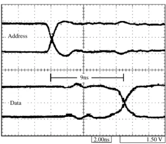
the process and typical characteristics of the SRAM are listed in Table 1. Fig. 4 shows the waveforms of the address input and the data output at room tem-perature with a 3V supply voltage. Typical access time is 9ns at a supply voltage 3V and an output load capacitance of 30pF. Active current is 28mA at 100MHz under typical conditions.
IV. CONCLUSIONS
A new high-speed low-power current-mode sense amplifier is presented. It is based on the posi-tive feedback technique and its access time is unaf-fected by the bit-line and data-line capacitances. The static behavior of the new circuit is analyzed. Owing to the separated cross-coupled latch, it causes no DC current path in standby state, a very small voltage swing at the bit-line and data-line, and a low average power consumption in the read operation. Compara-tive evaluations show that the new circuit gives higher sensing speed and lower power consumption than the reported circuit.
A novel current-mode technique for high-speed low-power SRAM’s has been described. The new
0.7
0.5
0.3
1 2 3 4 5 6 7 8 9 10
bit line capacitance, pF conv. new sensing delay , ns av erage po wer dissipation, mW 5 4 3 2 1 0
Table 1 Process and SRAM characteristics
Technology 0.35um 1P2M CMOS Logic Process
Gate length 0.35um Gate oxide 7.5nm Configuration 32Kbx8 Supply voltage 3V
Address access time 9ns (30pF, 3V)
Active current 28mA (100MHz, 25°C)
Fig. 3 Sensing delay and average power dissipation against
data-line capacitance (−−−− delay; - - - - power)
Fig. 2 Sensing delay and average power dissipation against
bit-line capacitance (−−−− delay; - - - - power)
1 0.8 0.6 0.4 0.2 0 4 3 2 1 0 1 2 3 4 5 6 7 8 9 10
data line capacitance, pF conv. new sensing delay , ns av erage po wer dissipation, mW 9ns 2.00ns 1.50 V Data Address
Fig. 4 Typical address and output waveforms
370 Journal of the Chinese Institute of Engineers, Vol. 26, No. 3 (2003)
circuit technique, was proven to be useful through the evaluation of an experimental 32Kx8 SRAM chip fabricated using 0.35um process technology. The SRAM has an ultra-low power dissipation of 84mW at 100MHz under typical conditions. Typical access time is 9ns at a supply voltage of 3V and an output load capacitance of 30pF. The new current-mode sense amplifier is suitable to realize high-speed and low-power SRAM’s.
REFERENCES
Blalock, T. N., and Jaeger, R. C., 1991, “A High Speed Clamped Bit-line Current-mode Sense Amplifier,” IEEE Journal of Solid-State Circuits, Vol. SC-26, pp. 542-548.
Chee, P. Y., Liu, P. C., and Siek, L., 1992, “High-speed Hybrid Current-mode Sense Amplifier for CMOS SRAMs,” Electronics Letters, 23rd. Vol. 38, No.9, pp.871-873.
Itoh, K., Sasaki, K., and Nakagome, Y., 1995, “Trends in Low-power RAM Circuit Technologies,”
Proceedings of the IEEE, Vol. 83, pp. 524-543.
Seevinck, E., 1990, “A Current Sense-amplifier for Fast CMOS SRAMs,” Symposium on VLSI
Cir-cuits Digest Technical Papers, pp. 71-72.
Seevinck, E., Van Beers, P. J., and Ontrop, H., 1991, “Current-mode Techniques for High-speed VLSI Circuits with Application to Current Sense Amplifier for CMOS SRAMs,” IEEE Journal of
Solid-State Circuits, Vol. SC-26, pp. 525-536.
Shibata, N., 1996, “Current Sense Amplifier for Low-voltage Memories,” IEICE Transactions on
Electronics, Vol. E79-C, No. 8, pp. 1120-1130.
Wicht, B., Schmitt-Landseidel, D., Paul, S., and Sanders, A., 2001, “SRAM Current-sense Ampli-fier with Fully-compensated Bit-line Multi-plexer,” IEEE International Solid-State Circuits
Conference, Digest of Technical Papers, pp.
172-173.
Manuscript Received: Apr. 22, 2002 Revision Received: Sep. 28, 2002 and Accepted: Nov. 11, 2002