372 IEEE ELECTRON DEVICE LETTERS, VOL. 26, NO. 6, JUNE 2005
A Novel Process-Compatible Fluorination
Technique With Electrical Characteristic
Improvements of Poly-Si TFTs
Shen-De Wang, Student Member, IEEE, Wei-Hsiang Lo, Tzu-Yun Chang, and Tan-Fu Lei
Abstract—A process-compatible fluorine passivation technique
of poly-Si thin-film transistors (TFTs) was demonstrated by em-ploying a novel CF4plasma treatment. Introducing fluorine atoms into poly-Si films can effectively passivate the trap states near the SiO2/poly-Si interface. With fluorine incorporation, the electrical characteristics of poly-Si TFTs can be significantly improved including a steeper subthreshold slope, smaller threshold voltage, lower leakage current, higher field-effect mobility, and better On/Off current ratio. Furthermore, the CF4 plasma treatment also improves the reliability of poly-Si TFTs with respect to hot-carrier stress, which is due to the formation of strong Si–F bonds.
Index Terms—CF4 plasma, fluorine, fluorine passivation, poly-Si, process-compatible, reliability, TFTs.
I. INTRODUCTION
P
OLYSILICON THIN-FILM transistors (poly-Si TFTs) have attracted much attention due to the possibility of realizing the integration of driving circuits and pixel elements on one glass substrate, and the potential to accomplish the system-on-panel (SOP) [1]. High-performance poly-Si TFTs are required for this goal. A hydrogenation process has been utilized to reduce the trap states of poly-Si films to improve the device performance [2]. However, hydrogenated poly-Si TFTs suffer from a serious instability issue due to weak Si–H bonds, which will break easily under an electrical stress [3]. Using fluorine to passivate the trap states of poly-Si TFTs has been reported recently [4]–[6]. Strong Si–F bonds, more stable than Si–H bonds, can maintain the device performance under long-term electrical stress. Conventional fluorine ion implantation might be not suitable for large-sized glass sub-strate applications. Moreover, a subsequent high temperature annealing is required to activate the fluorine atoms and recover the defects created by ion implantation. However, high-temper-ature process is not compatible with current production due to the low-melting point of low-cost glass substrate. Kim et al. demonstrated the use of fluorinated oxide SiO F to serve as a diffusion source [7], [8]. However, an extra film deposition and etching are required. To date, although hydrogen-based plasma treatments have been widely investigated in poly-Si TFTs, thereManuscript received February 22, 2005; revised March 18, 2005. This work was supported by the National Science Council of Taiwan, R.O.C., under Con-tracts NSC 93-2215-E-009-003 and NSC 93-2215-E-009-036. The review of this letter was arranged by Editor J. Sin.
The authors are with the Department of Electronics Engineering and Institute of Electronics, National Chiao-Tung University, Hsinchu 300, Taiwan, R. O. C.
Digital Object Identifier 10.1109/LED.2005.848095
is still a lack of an investigation of the fluorine-based plasma treatment.
In this letter, a novel fluorination technique is proposed by employing a low-temperature CF plasma treatment. This technique provides a simple, effective and process-compat-ible method to introduce fluorine atoms into poly-Si films and high-performance and high-reliability poly-Si TFTs were fabricated.
II. EXPERIMENTAL
The schematic diagram of fabrication processes is illustrated in Fig. 1. First, a 100-nm-thick amorphous silicon layer was deposited on a thermally oxidized Si wafer by dissociation of SiH gas in a low-pressure chemical vapor deposition (LPCVD) system at 550 C. Next, a semi-Gaussian-shaped KrF excimer laser nm at an energy density of 420 mJ/cm was performed for the phase transformation from amorphous to polycrystalline silicon. The average grain size of the poly-Si measured using scanning electron microcscopy (SEM) is approximately 300 nm, as shown in Fig. 1(b). Indi-vidual active regions were then patterned and defined. After the clean process, the samples were subjected to the CF plasma treatment, conducted in a plasma-enhanced chemical vapor de-position (PECVD) system at 350 C for 15 s, under a pressure of 200 mtorr and a power of 10 W, followed by a deposition of 100-nm-thick TEOS oxide by PECVD at 350 C. Then, a 200-nm-thick poly-Si was deposited by LPCVD at 620 C to serve as the gate electrode. A self-aligned phosphorous ion implantation was preformed at the dosage and energy of cm and 40 keV, respectively. The dopant activation was performed by excimer laser annealing (ELA), followed by a deposition of passivation layer and the definition of contact holes. Finally, a 500-nm-thick Al electrode was deposited and patterned. For comparison, the control TFTs were prepared without the CF plasma treatment process. No hydrogenation and thermal annealing process were performed after the Al formation.
III. RESULTS ANDDISCUSSION
There was no significant surface contamination on the poly-Si samples after chemical cleaning detected using total reflection X-ray fluorescence (TRXRF). Also, the variation of the thickness of the poly-Si films before and after CF plasma treatment measured using ellipsometer was within 5%. There-fore, the surface cleaning effect and the thinning effect of the
WANG et al.: NOVEL PROCESS-COMPATIBLE FLUORINATION TECHNIQUE 373
Fig. 1. Schematic diagram of the fabrication process of poly-Si TFT with CF plasma treatment. (a) Depositing amorphous silicon and ELA processing. (b) SEM image of ELA-processed poly-Si film after secco-etch. (c) Defining active region and CF plasma treatment. (d) S/D implantation and dopand activation by ELA. (e) Depositing passivation oxide, opening contact holes, depositing metal, and patterning metal.
Fig. 2. SIMS profiles of conventional and CF plasma-treated poly-Si films. Inset shows the FTIR spectra of the control and the CF plasma-treated poly-Si films.
CF plasma treated poly-Si films were excluded in this exper-iment. Fig. 2 shows the SIMS profiles of the control and CF plasma-treated poly-Si films. Fluorine atoms are introduced into the SiO /poly-Si interface by the CF plasma treatment. These piled-up fluorine atoms can provide an effective trap states termination, because the channel is formed near the interface. The inset shows the Fourier transform infrared spectroscopy (FTIR) spectra of the control and CF plasma-treated poly-Si samples. The spectra exhibit absorption peaks corresponding to Si-F bonds centered at round 940 cm [9], [10]. The strong peak of Si–O bond is related to the SiO substrate. Therefore, Si–F bonds were formed in the poly-Si by employing the CF plasma treatment.
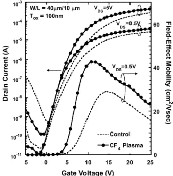
Fig. 3 shows the transfer characteristics and field-effect mo-bility versus the gate voltage for the devices. The measurements were performed at and 5 V. The threshold voltage
Fig. 3. Transfer characteristics and field-effect mobility versus gate voltage for the control and the CF plasma-treated poly-Si TFTs withV = 0:5 and 5 V.
was defined as the gate voltage required to achieve a
nor-malized drain current of at V.
Accordingly, the and the subthreshold slope of the CF plasma-treated TFT are 4.35 V and 1.28 V/dec., respec-tively, which are superior to 5.75 V and 1.92 V/dec. of the con-trol TFT. Notably, the leakage current of the CF plasma treated TFT is more than one order in magnitude lower than that of the control TFT, especially under a large negative gate bias. The corresponding On/Off current ratios for the CF plasma-treated poly-Si TFT and the control TFT are and
at V, respectively. The On/Off current ratio of the CF plasma-treated TFT is approximately eight times larger than that
374 IEEE ELECTRON DEVICE LETTERS, VOL. 26, NO. 6, JUNE 2005
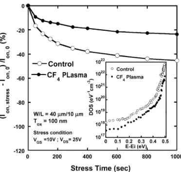
Fig. 4. On-current variations as a function of stress time under a hot carrier stress for the control and the CF plasma-treated poly-Si TFTs. Inset shows the density of states (DOS) in the energy bandgap of the control and the CF plasma-treated TFTs.
of the control TFT. Additionally, the CF plasma-treated TFT has an about 50% enhancement in the maximum field-effect mo-bility. Note that great improvements on device characteristics were obtained even though the conditions of ELA were not op-timized, which resulted in the rather poor field-effect mobility compared with other reports.
In order to verify the passivation effect of the CF plasma treatment, the effective trap states densities near the SiO /poly-Si interface were calculated form the . By ne-glecting the depletion capacitance, the can be expressed as [11]
(1) where the is the capacitance of the gate oxide. The of the control TFT and the CF plasma treated TFT are
cm and cm , respectively. The values reflect both interface sates and grain boundary trap states near the SiO /poly-Si interface. Therefore, those states near the SiO /poly-Si interface can be effectively terminated using CF plasma treatment. Combined with the SIMS profiles, we believe that the passivation effect is due to the piled-up fluorine atoms.
As shown in the inset of Fig. 4, the density of states (DOS) in the energy bandgap of the TFTs were calculated using field-effect conductance method [12]. Both deep states and tail states are significantly reduced using the CF plasma treatment. We deduce that for the control TFT, there exists lots of dangling bonds and strain bonds near the SiO /poly-Si interface, resulting in high deep states and tail states [13]. On the contrary, for the CF plasma treated TFT, fluorine atoms were introduced into the SiO /poly-Si network to terminate the dangling bonds, release
the strain bonds and form the S–F bonds, improving the device characteristics [5].
Additionally, hot carrier stress was carried out at
and for 1000 s to examine the device reliability. Fig. 4 shows the variations of the On-current under hot carrier stress. The degradation rate of the control is almost twice that of the CF plasma treated TFT. It is attributed to the strong Si–F bonds formed at the SiO /poly-Si interface. The Si–F bonds are hard to be broken under hot carrier stress, leading to a great improvement in the device reliability.
IV. CONCLUSION
Significant improvements on the device performance, in-cluding threshold voltage, subthreshold slope, leakage current, field-effect mobility, and On/Off current ratio have been demon-strated. This is due to the reduction of the interface states and grain boundary trap states near the SiO /poly-Si interface. The CF plasma treatment also improves the hot-carrier immunity due to the formation of Si-F bonds. It is concluded that the CF plasma treatment is a simple, effective and process-compatible method to fabricate high-performance and high-reliability poly-Si TFTs.
REFERENCES
[1] T. Serikawa, S. Shirai, A. Okamoto, and S. Suyama, “Low-temperature fabrication of high-mobility poly-Si TFTs for large-area LCDs,” IEEE Trans. Electron Devices, vol. 36, no. 9, pp. 1929–1933, Sep. 1989. [2] I. W. Wu, W. B. Jackson, T. Y. Huang, A. G. Lewis, and A. C. Chiang,
“Passivation kinetics of two types of defects in polysilicon TFT by plasma hydrogenation,” IEEE Electron Devices Lett., vol. 12, no. 5, pp. 181–183, May 1991.
[3] M. Hack, A. G. Lewis, and I.-W. Wu, “Physical models for degradation effects in polysilicon thin-film transistors,” IEEE Trans. Electron De-vices, vol. 40, no. 5, pp. 890–897, May 1993.
[4] H. N. Chern, C. L. Lee, and T. F. Lei, “The effects of fluorine passivation on polysilicon thin film transistors,” IEEE Trans. Electron Devices, vol. 41, no. 5, pp. 698–702, May 1994.
[5] S. Maegawa, T. Ipposhi, S. Maeda, H. Nishimura, T. Ichiki, M. Ashida, O. Tanina, Y. Inoue, T. Nishimura, and N. Tsubouchi, “Performance and reliability improvements in poly-Si TFTs by fluorine implantation into gate poly-Si,” IEEE Trans. Electron Devices, vol. 42, no. 6, pp. 1106–1111, Jun. 1995.
[6] J. W. Park, B. T. Ahn, and K. Lee, “Effects ofF implantation on the characteristics of poly-Si films and low-temperature n-ch poly-Si thin-film transistors,” Jpn. J. Appl. Phys., vol. 34, pp. 1436–1441, Mar. 1995.
[7] C. H. Kim, J. H. Jeon, J. S. Yoo, K. C. Park, and M. K. Han, “Excimer-laser-induced in situ fluorine passivation effects on polycrystalline sil-icon thin film transistors,” Jpn. J. Appl. Phys., vol. 38, pp. 2247–2250, Apr. 1999.
[8] C. H. Kim, S. H. Jung, J. S. Yoo, and M. K. Han, “Poly-Si TFT fabricated by laser-induced in situ fluorine passivation and laser doping,” IEEE Electron Devices Lett., vol. 22, no. 8, pp. 396–398, Aug. 2001. [9] Y. H. Kim, M. S. Hwang, and H. J. Kim, “Infrared spectroscopy study of
low-dielectric-constant fluorine-incorporated and carbon-incorporated silicon oxide films,” J. Appl. Phys., vol. 90, pp. 3367–3370, Oct. 2001. [10] S. Lee and J.-W. Park, “Effect of fluorine on dielectric properties of SiOF
films,” J. Appl. Phys., vol. 80, pp. 5260–5263, Nov. 1996.
[11] C. A. Dimitriadis, P. A. Coxon, L. Dozsa, L. Papadimitriou, and N. Economou, “Performance of thin-film transistors on polysilicon films grown by low-pressure chemical vapor deposition at various pressures,” IEEE Trans. Electron Devices, vol. 39, pp. 598–606, Mar. 1992. [12] G. Fortunato and P. Migliorato, “Determination of gap state density in
polycrystalline silicon by field-effect conductance,” Appl. Phys. Lett., vol. 49, pp. 1025–1027, Oct. 1986.
[13] M. Cao, T. J. King, and K. C. Saraswat, “Determination of the densi-ties of the gap states in hydrogenated polycrystalline Si andSi Ge films,” Appl. Phys. Lett., vol. 61, pp. 672–674, Aug. 1992.