Actel HDL Coding
Style Guide
© 2009 Actel Corporation. All rights reserved. Printed in the United States of America Part Number: 5029105-8
Release: July 2009
No part of this document may be copied or reproduced in any form or by any means without prior written consent of Actel.
Actel makes no warranties with respect to this documentation and disclaims any implied warranties of merchantability or fitness for a particular purpose. Information in this document is subject to change without notice. Actel assumes no responsibility for any errors that may appear in this document. This document contains confidential proprietary information that is not to be disclosed to any unauthorized person without prior written consent of Actel Corporation.
Trademarks
Actel and the Actel logo are registered trademarks of Actel Corporation. Adobe and Acrobat Reader are registered trademarks of Adobe Systems, Inc.
All other products or brand names mentioned are trademarks or registered trademarks of their respective holders.
Table of Contents
Introduction . . . 5
Document Organization . . . . 5
Document Assumptions . . . . 5
Document Conventions . . . . 5
HDL Keywords and Naming Conventions . . . . 6
Your Comments . . . . 7
Related Manuals . . . . 7
Online Help . . . . 8
1 Design Flow . . . 9
Design Flow Overview . . . . 9
2 Technology Independent Coding Styles . . . . 13
Sequential Devices . . . 13
Operators . . . 23
Datapath . . . 24
Finite State Machine . . . 37
Input-Output Buffers . . . 44
Generics and Parameters . . . 48
3 Performance Driven Coding . . . . 51
Reducing Logic Levels on Critical Paths . . . . 51
Resource Sharing . . . 53
Operators Inside Loops . . . 54
Coding for Combinability . . . 55
Register Duplication . . . 56
Partitioning a Design . . . 58
4 Technology Specific Coding Techniques . . . . 61
Multiplexors . . . 61
Internal Tri-State to Multiplexor Mapping . . . 61
Registers . . . 63
Registered I/Os . . . 68
CLKINT/CLKBUF for Reset and/or High Fanout Networks . . . 69
QCLKINT/QCLKBUF for Medium Fanout Networks . . . 71
SmartGen Counter . . . 71
Dual Architecture Coding in VHDL . . . 73
SRAM . . . 75
FIFO . . . 80
Actel Technical Support . . . 87
Website . . . 87
Contacting the Customer Technical Support Center . . . 87
Introduction
VHDL and Verilog® HDL are high level description languages for system and circuit design. These languages support
various abstraction levels of design, including architecture-specific design. At the higher levels, these languages can be used for system design without regard to a specific technology. To create a functional design, you only need to consider a specific target technology. However, to achieve optimal performance and area from your target device, you must become familiar with the architecture of the device and then code your design for that architecture.
Efficient, standard HDL code is essential for creating good designs. The structure of the design is a direct result of the structure of the HDL code. Additionally, standard HDL code allows designs to be reused in other designs or by other HDL designers.
This document provides the preferred coding styles for the Actel architecture. The information is reference material with instructions to optimize your HDL code for the Actel architecture. Examples in both VHDL and Verilog code are provided to illustrate these coding styles and to help implement the code into your design.
For further information about HDL coding styles, synthesis methodology, or application notes, please visit Actel’s web site at the following URL: http://www.actel.com/
Document Organization
The Actel HDL Coding Style Guide is divided into the following chapters:
Chapter 1 - Design Flow describes the basic design flow for creating Actel designs with HDL synthesis and simulation
tools.
Chapter 2 - Technology Independent Coding Styles describes basic high level HDL coding styles and techniques. Chapter 3 - Performance Driven Coding illustrates efficient design practices and describes synthesis implementations
and techniques that can be used to reduce logic levels on a critical path.
Chapter 4 - Technology Specific Coding Techniques describes how to implement technology specific features and
technology specific cores for optimal area and performance utilization.
Appendix A - Product Support provides information about contacting Actel for customer and technical support.
Document Assumptions
The information in this manual is based on the following assumptions:
• You are familiar with Verilog or VHDL hardware description language, and HDL design methodology for designing logic circuits.
• You are familiar with FPGA design software, including design synthesis and simulation tools.
Document Conventions
The following conventions are used throughout this manual. Information input by the user follows this format:
keyboard input
The contents of a file follows this format:
file contents
HDL code appear as follows, with HDL keyword in bold:
entity actel is port (
end actel;
Messages that are displayed on the screen appear as follows:
HDL Keywords and Naming Conventions
There are naming conventions you must follow when writing Verilog or VHDL code. Additionally, Verilog and VHDL have reserved words that cannot be used for signal or entity names. This section lists the naming conventions and reserved keywords for each.
VHDL
The following naming conventions apply to VHDL designs: • VHDL is not case sensitive.
• Two dashes “--” are used to begin comment lines.
• Names can use alphanumeric characters and the underscore “_” character. • Names must begin with an alphabetic letter.
• You may not use two underscores in a row, or use an underscore as the last character in the name. • Spaces are not allowed within names.
• Object names must be unique. For example, you cannot have a signal named A and a bus named A(7 downto 0). The following is a list of the VHDL reserved keywords:
Screen Message
abs downto library postponed subtype
access else linkage procedure then
after elsif literal process to
alias end loop pure transport
all entity map range type
and exit mod record unaffected
architecture file nand register units
array for new reject until
assert function next rem use
attribute generate nor report variable
begin generic not return wait
block group null rol when
body guarded of ror while
buffer if on select with
bus impure open severity xnor
case in or shared xor
component inertial others signal
configuration inout out sla
constant is package sra
Your Comments
Verilog
The following naming conventions apply to Verilog HDL designs: • Verilog is case sensitive.
• Two slashes “//” are used to begin single line comments. A slash and asterisk “/*” are used to begin a multiple line comment and an asterisk and slash “*/” are used to end a multiple line comment.
• Names can use alphanumeric characters, the underscore “_” character, and the dollar “$” character. • Names must begin with an alphabetic letter or the underscore.
• Spaces are not allowed within names.
The following is a list of the Verilog reserved keywords:
Your Comments
Actel Corporation strives to produce the highest quality online help and printed documentation. We want to help you learn about our products, so you can get your work done quickly. We welcome your feedback about this guide and our online help. Please send your comments to documentation@actel.com.
Related Manuals
The following manuals provide additional information about designing and programming Actel FPGAs using HDL design methodology:
always endmodule medium reg tranif0
and endprimitive module release tranif1
assign endspecify nand repeat tri
attribute endtable negedge rnmos tri0
begin endtask nmos rpmos tri1
buf event nor rtran triand
bufif0 for not rtranif0 trior
bufif1 force notif0 rtranif1 trireg
case forever notif1 scalared unsigned
casex fork or signed vectored
casez function output small wait
cmos highz0 parameter specify wand
deassign highz1 pmos specparam weak0
default if posedge strength weak1
defparam ifnone primitive strong0 while
disable initial pull0 strong1 wire
edge inout pull1 supply0 wor
else input pulldown supply1 xnor
end integer pullup table xor
endattribute join remos task
endcase large real time
HDL Chip Design. Smith, Douglas J. Madison, AL: Doone Publications, 1996. This book describes and gives examples of how to design FPGAs using VHDL and Verilog.
IEEE Standard VHDL Language Reference Manual. New York: Institute of Electrical and Electronics Engineers, Inc., 1994. This manual specifies IEEE Standard 1076-1993, which defines the VHDL standard and the use of VHDL in the creation of electronic systems.
Online Help
1
Design Flow
This chapter illustrates and describes the basic design flow for creating Actel designs using HDL synthesis and simulation tools.
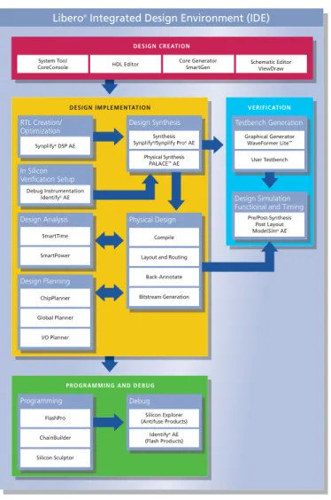
Figure 1-1 illustrates the HDL synthesis-based design flow for an Actel FPGA using third party CAE tools and Designer software.
Design Flow Overview
The Actel HDL synthesis-based design flow has four main steps: design creation/verification, design implementation, programming, and system verification. These steps are described in detail in the following sections.
Figure 1-1 · Actel HDL Synthesis-Based Design Flow
Libero® Integrated Design Environment (IDE)
D E S I G N I M P L E M E N TAT I O N P R O G R A M M I N G A N D D E B U G In Silicon Verification Setup Debug Instrumentation Identify® AE Design Analysis SmartTime SmartPower Design Planning ChipPlanner Global Planner I/O Planner Programming FlashPro ChainBuilder Silicon Sculptor RTL Creation/ Optimization Synplify® DSP AE Design Simulation Functional and Timing
Pre/Post-Synthesis Post Layout ModelSim® AE Testbench Generation Graphical Generator WaveFormer Lite™ User Testbench Design Synthesis Synthesis Synplify®/Synplify Pro® AE
Physical Synthesis PALACE™ AE Debug Silicon Explorer (Antifuse Products) Identify® AE (Flash Products) V E R I F I C AT I O N Physical Design Compile Layout and Routing
Back-Annotate Bitstream Generation D E S I G N C R E AT I O N System Tool CoreConsole Core Generator SmartGen
HDL Editor Schematic Editor ViewDraw
Design Creation/Verification
During design creation/verification, a design is captured in an RTL-level (behavioral) HDL source file. After capturing the design, a behavioral simulation of the HDL file can be performed to verify that the HDL code is correct. The code is then synthesized into an Actel gate-level (structural) HDL netlist. After synthesis, a structural simulation of the design can be performed. Finally, an EDIF netlist is generated for use in Designer and an HDL structural netlist is generated for timing simulation.
HDL Design Source Entry
Enter your HDL design source using a text editor or a context-sensitive HDL editor. Your HDL source file can contain RTL-level constructs, as well as instantiations of structural elements, such as SmartGen cores.
Behavioral Simulation
You can perform a behavioral simulation of your design before synthesis. Behavioral simulation verifies the functionality of your HDL code. Typically, unit delays are used and a standard HDL test bench can be used to drive simulation. Refer to the documentation included with your simulation tool for information about performing behavioral simulation.
Synthesis
After you have created your behavioral HDL source file, you must synthesize it before placing and routing it in Designer. Synthesis translates the behavioral HDL file into a gate-level netlist and optimizes the design for a target technology. Refer to the documentation included with your synthesis tool for information about performing design synthesis.
Netlist Generation
After you have created, synthesized, and verified your design, you may place-and-route in Designer using an EDIF, Verilog, or VHDL netlist. This netlist is also used to generate a structural HDL netlist for use in structural simulation. Refer to the Designer Series documentation for information about generating a netlist.
Structural Netlist Generation
You can generate a structural HDL netlist from your EDIF netlist for use in structural simulation by either exporting it from Designer or by using the Actel “edn2vhdl” or “edn2vlog” program. Refer to the Designer Series documentation for information about generating a structural netlist.
Structural Simulation
You can perform a structural simulation of your design before placing and routing it. Structural simulation verifies the functionality of your post-synthesis structural HDL netlist. Default unit delays included in the compiled Actel VITAL libraries are used for every gate. Refer to the documentation included with your simulation tool for information about performing structural simulation.
Design Implementation
During design implementation, a design is placed-and-routed using Designer. Additionally, timing analysis is performed on a design in Designer with the Timer tool. After place-and-route, post-layout (timing) simulation is performed.
Place-and-Route
Use Designer to place-and-route your design. Refer to the Designer software online help for information about using
Designer.
Timing Analysis
Use the SmartTime tool in Designer to perform static timing analysis on your design. Refer to the online help for
Design Flow Overview
Timing Simulation
After placing-and-routing your design, you perform a timing simulation to verify that the design meets timing constraints. Timing simulation requires timing information exported from Designer, which overrides default unit delays in the compiled Actel VITAL libraries. Refer to the Designer Series documentation for information about exporting timing information from Designer.
Programming
Programming a device requires software and hardware from Actel or a supported 3rd party programming system. Refer
to the Actel web site, www.actel.com, for information on programming an Actel device.
System Verification
You can perform system verification on a programmed device using Actel’s Silicon Explorer. Refer to Silicon Explorer II Quick Start for information on using Silicon Explorer.
2
Technology Independent Coding Styles
This chapter describes basic HDL coding styles and techniques. These coding styles are essential when writing efficient, standard HDL code and creating technology independent designs.
Sequential Devices
A sequential device, either a flip-flop or a latch, is a one-bit memory device. A latch is a level-sensitive memory device and a flip-flop is an edge-triggered memory device.
Flip-Flops (Registers)
Flip-flops, also called registers, are inferred in VHDL using wait and if statements within a process using either a rising edge or falling edge detection expression. There are two types of expressions that can be used, a 'event attribute or a function call. For example:
(clk'event and clk='1') --rising edge 'event attribute (clk'event and clk='0') --falling edge 'event attribute rising_edge(clock) --rising edge function call falling_edge(clock) --falling edge function call
The examples in this guide use rising edge 'event attribute expressions, but falling edge expressions could be used. The 'event attribute expression is used because some VHDL synthesis tools may not recognize function call expressions. However, using a function call expression is preferred for simulation because a function call only detects an edge transition (0 to 1 or 1 to 0) but not a transition from X to 1 or 0 to X, which may not be a valid transition. This is especially true if using a multi-valued data type like std_logic, which has nine possible values (U, X, 0, 1, Z, W, L, H, -). This section describes and gives examples for different types of flip-flops. Refer to “Registers” on page 63 for additional information about using specific registers in the Actel architecture.
Rising Edge Flip-Flop
The following examples infer a D flip-flop without asynchronous or synchronous reset or preset. This flip-flop is a basic sequential cell in the Actel antifuse architecture.
VHDL
library IEEE;
use IEEE.std_logic_1164.all; entity dff is
port (data, clk : in std_logic;
q : out std_logic);
end dff;
architecture behav of dff is begin
Figure 2-1. D Flip Flop
data
clk
q <= data; end if; end process; end behav; Verilog module dff (data, clk, q); input data, clk; output q; reg q; always @(posedge clk) q = data; endmodule
Rising Edge Flip-Flop with Asynchronous Reset
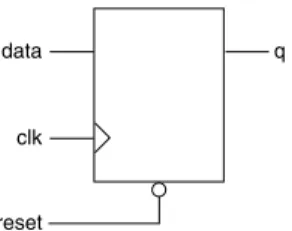
The following examples infer a D flip-flop with an asynchronous reset. This flip-flop is a basic sequential cell in the Actel antifuse architecture.
VHDL
library IEEE;
use IEEE.std_logic_1164.all; entity dff_async_rst is
port (data, clk, reset : in std_logic;
q : out std_logic);
end dff_async_rst;
architecture behav of dff_async_rst is begin
process (clk, reset) begin if (reset = '0') then
q <= '0';
elsif (clk'event and clk = '1') then
q <= data;
end if; end process; end behav;
Verilog
module dff_async_rst (data, clk, reset, q); input data, clk, reset;
output q; reg q;
always @(posedge clk or negedge reset) if (~reset)
Figure 2-2 · D Flip-Flop with Asynchronous Reset
data
clk
q
Sequential Devices
q = 1'b0;
else
q = data;
endmodule
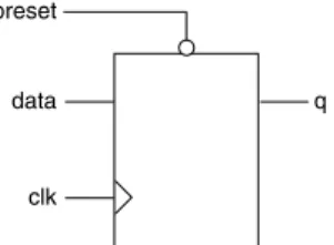
Rising Edge Flip-Flop with Asynchronous Preset
The following examples infer a D flip-flop with an asynchronous preset. Refer to “Registers” on page 63 for additional information about using preset flip-flops with the Actel architecture.
VHDL
library IEEE;
use IEEE.std_logic_1164.all; entity dff_async_pre is
port (data, clk, preset : in std_logic;
q : out std_logic);
end dff_async_pre;
architecture behav of dff_async_pre is begin
process (clk, preset) begin if (preset = '0') then
q <= '1';
elsif (clk'event and clk = '1') then
q <= data;
end if; end process; end behav;
Verilog
module dff_async_pre (data, clk, preset, q); input data, clk, preset;
output q; reg q;
always @(posedge clk or negedge preset) if (~preset)
q = 1'b1;
else
q = data;
endmodule
Figure 2-3. D Flip-Flop with Asynchronous Preset
data
clk
q preset
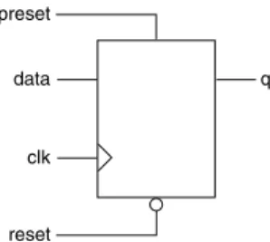
Rising Edge Filp-Flop with Asynchronous Reset and Preset
The following examples infer a D flip-flop with an asynchronous reset and preset. Refer to “Registers” on page 63 for additional information about using preset flip-flops with the Actel architecture.
VHDL
library IEEE;
use IEEE.std_logic_1164.all; entity dff_async is
port (data, clk, reset, preset : in std_logic;
q : out std_logic);
end dff_async;
architecture behav of dff_async is begin
process (clk, reset, preset) begin if (reset = '0') then
q <= '0';
elsif (preset = '1') then
q <= '1';
elsif (clk'event and clk = '1') then
q <= data;
end if; end process; end behav;
Verilog
module dff_async (reset, preset, data, q, clk); input clk;
input reset, preset, data; output q;
reg q;
always @ (posedge clk or negedge reset or posedge preset) if (~reset) q = 1'b0; else if (preset) q = 1'b1; else q = data; endmodule
Figure 2-4 · D Flip-Flop with Asynchronous Reset and Preset
data
clk preset
q
Sequential Devices
Rising Edge Flip-Flop with Synchronous Reset
The following examples infer a D flip-flop with a synchronous reset.
VHDL
library IEEE;
use IEEE.std_logic_1164.all; entity dff_sync_rst is
port (data, clk, reset : in std_logic;
q : out std_logic);
end dff_sync_rst;
architecture behav of dff_sync_rst is begin
process (clk) begin
if (clk'event and clk = '1') then if (reset = '0') then q <= '0'; else q <= data; end if; end if; end process; end behav; Verilog
module dff_sync_rst (data, clk, reset, q); input data, clk, reset;
output q; reg q; always @ (posedge clk) if (~reset) q = 1'b0; else q = data; endmodule
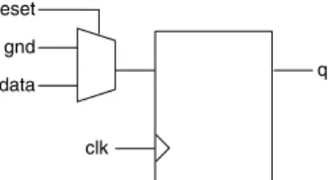
Figure 2-5 · D Flip-Flop with Synchronous Reset
data gnd
clk reset
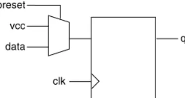
Rising Edge Flip-Flop with Synchronous Preset
The following examples infer a D flip-flop with a synchronous preset.
VHDL
library IEEE;
use IEEE.std_logic_1164.all; entity dff_sync_pre is
port (data, clk, preset : in std_logic;
q : out std_logic);
end dff_sync_pre;
architecture behav of dff_sync_pre is begin
process (clk) begin
if (clk'event and clk = '1') then
if (preset = '0') then q <= '1'; else q <= data; end if; end if; end process; end behav; Verilog
module dff_sync_pre (data, clk, preset, q); input data, clk, preset;
output q; reg q; always @ (posedge clk) if (~preset) q = 1'b1; else q = data; endmodule
Figure 2-6. D Flip-Flop with Synchronous Preset
data vcc
clk preset
Sequential Devices
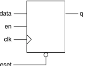
Rising Edge Flip-Flop with Asynchronous Reset and Clock Enable
The following examples infer a D type flip-flop with an asynchronous reset and clock enable.
VHDL
library IEEE;
use IEEE.std_logic_1164.all; entity dff_ck_en is
port (data, clk, reset, en : in std_logic;
q : out std_logic);
end dff_ck_en;
architecture behav of dff_ck_en is begin
process (clk, reset) begin if (reset = '0') then
q <= '0';
elsif (clk'event and clk = '1') then if (en = '1') then q <= data; end if; end if; end process; end behav; Verilog
module dff_ck_en (data, clk, reset, en, q); input data, clk, reset, en;
output q; reg q;
always @ (posedge clk or negedge reset) if (~reset) q = 1'b0; else if (en) q = data; endmodule
D-Latches
This section describes and gives examples of different types of D-latches.
Figure 2-7 · D Flip-Flop with Asynchronous Reset and Clock Enable
data en clk
q
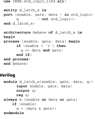
D-Latch with Data and Enable
The following examples infer a D-latch with data and enable inputs.
VHDL
library IEEE;
use IEEE.std_logic_1164.all; entity d_latch is
port(enable, data: in std_logic;
y : out std_logic);
end d_latch;
architecture behave of d_latch is begin
process (enable, data) begin if (enable = '1') then y <= data; end if; end process; end behave; Verilog
module d_latch (enable, data, y); input enable, data;
output y; reg y;
always @(enable or data) if (enable)
y = data;
endmodule
D-Latch with Gated Asynchronous Data
The following examples infer a D-latch with gated asynchronous data.
VHDL
library IEEE;
Figure 2-8. D-Latch
Figure 2-9 · D-Latch with Gated Asynchronous Data
data enable y data enable q gate
Sequential Devices
use IEEE.std_logic_1164.all; entity d_latch_e is
port (enable, gate, data : in std_logic;
q : out std_logic);
end d_latch_e;
architecture behave of d_latch_e is begin
process (enable, gate, data) begin if (enable = '1') then
q <= data and gate;
end if; end process; end behave;
Verilog
module d_latch_e(enable, gate, data, q); input enable, gate, data;
output q; reg q;
always @ (enable or data or gate) if (enable)
q = (data & gate);
endmodule
D-Latch with Gated Enable
The following examples infer a D-latch with gated enable.
VHDL
library IEEE;
use IEEE.std_logic_1164.all; entity d_latch_en is
port (enable, gate, d: in std_logic;
q : out std_logic);
end d_latch_en;
architecture behave of d_latch_en is begin
process (enable, gate, d) begin
if ((enable and gate) = '1') then
q <= d;
end if; end process;
Figure 2-10 · D-Latch with Gated Enable
enable
d q
Verilog
module d_latch_en(enable, gate, d, q); input enable, gate, d;
output q; reg q;
always @ (enable or d or gate) if (enable & gate)
q = d;
endmodule
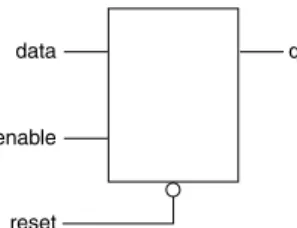
D-Latch with Asynchronous Reset
The following examples infer a D-latch with an asynchronous reset.
VHDL
library IEEE;
use IEEE.std_logic_1164.all; entity d_latch_rst is
port (enable, data, reset: in std_logic;
q : out std_logic);
end d_latch_rst;
architecture behav of d_latch_rst is begin
process (enable, data, reset) begin if (reset = '0') then
q <= '0';
elsif (enable = '1') then
q <= data;
end if; end process; end behav;
Verilog
module d_latch_rst (reset, enable, data, q); input reset, enable, data;
output q; reg q;
always @ (reset or enable or data) if (~reset)
q = 1'b0;
else if (enable)
q = data;
endmodule
Figure 2-11 · D-Latch with Asynchronous Reset
data
enable
reset
Operators
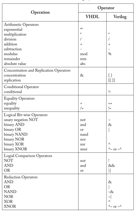
Operators
A number of bit-wise operators are available to you: Arithmetic, Concentration and Replication, Conditional, Equality, Logical Bit-wise, Logical Comparison, Reduction, Relational, Shift, and Unary Arithmetic (Sign). These operators and their availability in VHDL or Verilog are compared in Table 2-1.
Table 2-1 · VHDL and Verilog Operators
Operation Operator VHDL Verilog Arithmetic Operators exponential multiplication division addition subtraction modulus remainder absolute value ** * / + -mod rem abs * / + -%
Concentration and Replication Operators concentration replication & { } {{ }} Conditional Operator conditional ?: Equality Operators equality inequality = /= == != Logical Bit-wise Operators
unary negation NOT binary AND binary OR binary NAND binary NOR binary XOR binary XNOR not and or nand nor xor xnor ~ & | ^ ^~ or ~^ Logial Comparison Operators
NOT AND OR not and or ! && || Reduction Operators AND OR NAND NOR XOR XNOR & | ~& ~| ^ ^~ or ~^
Datapath
Datapath logic is a structured repetitive function. These structures are modeled in various different implementations based on area and timing constraints. Most synthesis tools generate optimal implementations for the target technology.
Priority Encoders Using If-Then-Else
An if-then-else statement is used to conditionally execute sequential statements based on a value. Each condition of the if-then-else statement is checked in order against that value until a true condition is found. Statements associated with the true condition are then executed and the rest of the statement is ignored. If-then-else statements should be used to imply priority on a late arriving signal. In the following examples, shown in Figure 2-12, signal c is a late arriving signal.
VHDL
library IEEE;
use IEEE.std_logic_1164.all;
Relational Operators less than
less than or equal to greater than
greater than or equal to
< <= > >= < <= > >= Shift Operators
logical shift left logical shift right arithmetic shift left arithmetic shift right logical rotate left logical rotate right
sll srl sla sra rol ror << >>
Unary Arithmetic Operators identity negotiation + -+ -Table 2-1 · VHDL and Verilog Operators (continued)
Operation Operator
VHDL Verilog
Figure 2-12 · Priority Encoder Using an If-Then-Else Statement
f e d c s=10 s=01 s=00 pout Three C modules
Datapath
entity my_if is
port (c, d, e, f: in std_logic;
s : in std_logic_vector(1 downto 0); pout : out std_logic);
end my_if;
architecture my_arc of my_if is begin
myif_pro: process (s, c, d, e, f) begin
if s = “00” then pout <= c; elsif s = “01” then pout <= d; elsif s = “10” then pout <= e; else pout <= f; end if;
end process myif_pro; end my_arc;
Verilog
module IF_MUX (c, d, e, f, s, pout); input c, d, e, f; input [1:0]s; output pout; reg pout; always @(c or d or e or f or s) begin if (s == 2'b00) pout = c; else if (s ==2'b01) pout = d; else if (s ==2'b10) pout = e; else pout = f; end endmodule
Multiplexors Using Case
A case statement implies parallel encoding. Use a case statement to select one of several alternative statement sequences based on the value of a condition. The condition is checked against each choice in the case statement until a match is found. Statements associated with the matching choice are then executed. The case statement must include all possible values for a condition or have a default choice to be executed if none of the choices match. The following examples infer multiplexors using a case statement. Refer to “Multiplexors” on page 61 for additional information about using multiplexors with the Actel architecture.
VHDL synthesis tools automatically assume parallel operation without priority in case statements. However, some Verilog tools assume priority, and you may need to add a directive to your case statement to ensure that no priority is
assumed. refer to the documentation provided with your synthesis tool for information about creating case statements without priority.
4:1 Multiplexor
The following examples infer a 4:1 multiplexor using a case statement.
VHDL --4:1 Multiplexor library IEEE; use IEEE.std_logic_1164.all; entity mux is port (C, D, E, F : in std_logic; S : in std_logic_vector(1 downto 0); mux_out : out std_logic);
end mux;
architecture my_mux of mux is begin
mux1: process (S, C, D, E, F) begin
case s is
when “00” => muxout <= C; when “01” => muxout <= D; when “10” => muxout <= E; when others => muxout <= F; end case;
end process mux1; end my_mux;
Verilog
//4:1 Multiplexor
module MUX (C, D, E, F, S, MUX_OUT); input C, D, E, F; input [1:0] S; output MUX_OUT; reg MUX_OUT; always @(C or D or E or F or S) begin case (S) 2'b00 : MUX_OUT = C; 2'b01 : MUX_OUT = D; 2'b10 : MUX_OUT = E; default : MUX_OUT = F; endcase end endmodule
Figure 2-13 · Multiplexor Using a Case Statement
C F MUX_OUT D E MUX S(1:0)
Datapath
12:1 Multiplexor
The following examples infer a 12:1 multiplexor using a case statement.
VHDL -- 12:1 mux library ieee; use ieee.std_logic_1164.all; -- Entity declaration: entity mux12_1 is port (
mux_sel: in std_logic_vector (3 downto 0);-- mux select
A: in std_logic; B: in std_logic; C: in std_logic; D: in std_logic; E: in std_logic; F: in std_logic; G: in std_logic; H: in std_logic; I: in std_logic; J: in std_logic; K: in std_logic; M: in std_logic;
mux_out: out std_logic -- mux output );
end mux12_1;
-- Architectural body:
architecture synth of mux12_1 is begin
proc1: process (mux_sel, A, B, C, D, E, F, G, H, I, J, K, M)
begin case mux_sel is when "0000" => mux_out<= A; when "0001" => mux_out <= B; when "0010" => mux_out <= C; when "0011” => mux_out <= D; when "0100" => mux_out <= E; when "0101" => mux_out <= F; when "0110" => mux_out <= G; when "0111" => mux_out <= H; when "1000" => mux_out <= I; when "1001" => mux_out <= J; when "1010" => mux_out <= K; when "1011" => mux_out <= M;
when others => mux_out<= '0';
end case;
end process proc1; end synth;
Verilog // 12:1 mux module mux12_1(mux_out, mux_sel,M,L,K,J,H,G,F,E,D,C,B,A ); output mux_out; input [3:0] mux_sel; input M; input L; input K; input J; input H; input G; input F; input E; input D; input C; input B; input A; reg mux_out;
// create a 12:1 mux using a case statement
always @ ({mux_sel[3:0]} or M or L or K or J or H or G or F or E or D or C or B or A) begin: mux_blk
case ({mux_sel[3:0]}) // synthesis full_case parallel_case
4'b0000 : mux_out = A; 4'b0001 : mux_out = B; 4'b0010 : mux_out = C; 4'b0011 : mux_out = D; 4'b0100 : mux_out = E; 4'b0101 : mux_out = F; 4'b0110 : mux_out = G; 4'b0111 : mux_out = H; 4'b1000 : mux_out = J; 4'b1001 : mux_out = K; 4'b1010 : mux_out = L; 4'b1011 : mux_out = M; 4'b1100 : mux_out = 1'b0; 4'b1101 : mux_out = 1'b0; 4'b1110 : mux_out = 1'b0; 4'b1111 : mux_out = 1'b0; endcase end endmodule Case X Multiplexor
The following Verilog example infers a multiplexor using a don’t care case x statement. Actel does not recommend using don’t care case x statements in VHDL. VHDL synthesis tools do not typically support the don’t care value as well as Verilog tools.
Verilog
//8 bit 4:1 multiplexor with don't care X, 3:1 equivalent mux
module mux4 (a, b, c, sel, q); input [7:0] a, b, c;
input [1:0] sel; output [7:0] q; reg [7:0] q;
Datapath always @ (sel or a or b or c) casex (sel) 2'b00: q = a; 2'b01: q = b; 2'b1x: q = c; default: q = c; endcase endmodule
Decoders
Decoders are used to decode data that has been previously encoded using binary or another type of encoding. The following examples infer a 3-8 line decoder with an enable.
VHDL
library IEEE;
use IEEE.std_logic_1164.all; entity decode is
port ( Ain : in std_logic_vector (2 downto 0);
En: in std_logic;
Yout : out std_logic_vector (7 downto 0));
end decode;
architecture decode_arch of decode is begin process (Ain) begin if (En='0') then Yout <= (others => '0'); else case Ain is when "000" => Yout <= "00000001"; when "001" => Yout <= "00000010"; when "010" => Yout <= "00000100"; when "011" => Yout <= "00001000"; when "100" => Yout <= "00010000"; when "101" => Yout <= "00100000"; when "110" => Yout <= "01000000"; when "111" => Yout <= "10000000"; when others => Yout <= "00000000"; end case;
end if; end process; end decode_arch;
Verilog
module decode (Ain, En, Yout); input En;
input [2:0] Ain; output [7:0] Yout; reg [7:0] Yout; always @ (En or Ain)
else case (Ain) 3'b000 : Yout = 8'b00000001; 3'b001 : Yout = 8'b00000010; 3'b010 : Yout = 8'b00000100; 3'b011 : Yout = 8'b00001000; 3'b100 : Yout = 8'b00010000; 3'b101 : Yout = 8'b00100000; 3'b110 : Yout = 8'b01000000; 3'b111 : Yout = 8'b10000000; default : Yout = 8'b00000000; endcase end endmodule
Counters
Counters count the number of occurrences of an event that occur either randomly or at uniform intervals. You can infer a counter in your design. However, most synthesis tools cannot infer optimal implementations of counters higher than 8-bits. If your counter is in the critical path of a speed and area critical design, Actel recommends that you use the SmartGen Core Builder to build a counter. Once generated, instantiate the SmartGen counter in your design. Refer to
“SmartGen Counter” on page 71 for examples of SmartGen counter instantiation. The following examples infer different types of counters.
8-bit Up Counter with Count Enable and Asynchronous Reset
The following examples infer an 8-bit up counter with count enable and asynchronous reset.
VHDL library IEEE; use IEEE.std_logic_1164.all; use IEEE.std_logic_unsigned.all; use IEEE.std_logic_arith.all; entity counter8 is
port (clk, en, rst : in std_logic;
count : out std_logic_vector (7 downto 0));
end counter8;
architecture behav of counter8 is
signal cnt: std_logic_vector (7 downto 0); begin
process (clk, en, cnt, rst) begin
if (rst = '0') then
cnt <= (others => '0');
elsif (clk'event and clk = '1') then if (en = '1') then cnt <= cnt + '1'; end if; end process; count <= cnt; end behav; Verilog
module count_en (en, clock, reset, out); parameter Width = 8;
Datapath
output [Width-1:0] out; reg [Width-1:0] out;
always @(posedge clock or negedge reset) if(!reset)
out = 8'b0;
else if(en)
out = out + 1;
endmodule
8-bit Up Counter with Load and Asynchronous Reset
The following examples infer an 8-bit up counter with load and asynchronous reset.
VHDL library IEEE; use IEEE.std_logic_1164.all; use IEEE.std_logic_unsigned.all; use IEEE.std_logic_arith.all; entity counter is
port (clk, reset, load: in std_logic;
data: in std_logic_vector (7 downto 0); count: out std_logic_vector (7 downto 0));
end counter;
architecture behave of counter is
signal count_i : std_logic_vector (7 downto 0); begin
process (clk, reset) begin
if (reset = '0') then
count_i <= (others => '0');
elsif (clk'event and clk = '1') then if load = '1' then count_i <= data; else count_i <= count_i + '1'; end if; end if; end process; count <= count_i; end behave; Verilog
module count_load (out, data, load, clk, reset); parameter Width = 8;
input load, clk, reset; input [Width-1:0] data; output [Width-1:0] out; reg [Width-1:0] out;
always @(posedge clk or negedge reset) if(!reset)
out = 8'b0;
else if(load)
endmodule
8-bit Up Counter with Load, Count Enable, Terminal Count and Asynchronous Reset
The following examples infer an 8-bit up counter with load, count enable, terminal count, and asynchronous reset.
Verilog
module count_load (out, cout, data, load, clk, en, reset); parameter Width = 8;
input load, clk, en, reset; input [Width-1:0] data; output cout; // carry out output [Width-1:0] out; reg [Width-1:0] out;
always @(posedge clk or negedge reset) if(!reset) out = 8'b0; else if(load) out = data; else if(en) out = out + 1;
// cout=1 when all out bits equal 1
assign cout = &out; endmodule
N-bit Up Counter with Load, Count Enable, and Asynchronous Reset
The following examples infer an n-bit up counter with load, count enable, and asynchronous reset.
VHDL library IEEE; use IEEE.std_logic_1164.all; use IEEE.std_logic_unsigned.all; use IEEE.std_logic_arith.all; entity counter is
generic (width : integer := n);
port (data : in std_logic_vector (width-1 downto 0); load, en, clk, rst : in std_logic;
q : out std_logic_vector (width-1 downto 0));
end counter;
architecture behave of counter is
signal count : std_logic_vector (width-1 downto 0); begin
process(clk, rst) begin
if rst = '1' then
count <= (others => '0');
elsif (clk'event and clk = '1') then if load = '1' then count <= data; elsif en = '1' then count <= count + '1'; end if; end if; end process; q <= count;
Datapath
end behave;
Arithmetic Operators
Synthesis tools generally are able to infer arithmetic operators for the target technology. The following examples infer addition, subtraction, division and multiplication operators.
VHDL library IEEE; use IEEE.std_logic_1164.all; use IEEE.std_logic_arith.all; use IEEE.std_logic_unsigned.all; entity arithmetic is
port (A, B: in std_logic_vector(3 downto 0);
Q1: out std_logic_vector(4 downto 0); Q2, Q3: out std_logic_vector(3 downto 0); Q4: out std_logic_vector(7 downto 0));
end arithmetic;
architecture behav of arithmetic is begin
process (A, B) begin
Q1 <= ('0' & A) + ('0' & B); --addition Q2 <= A - B; --subtraction
Q3 <= A / B; --division Q4 <= A * B; --multiplication
end process; end behav;
If the multiply and divide operands are powers of 2, replace them with shift registers. Shift registers provide speed optimized implementations with large savings in area. For example:
Q <= C/16 + C*4;
can be represented as:
Q <= shr (C, “100”) + shl (C, “10”);
or
VHDL Q <= “0000” & C (8 downto 4) + C (6 downto 0) & ”00”;
The functions “shr” and “shl” are available in the IEEE.std_logic_arith.all library.
Verilog
module arithmetic (A, B, Q1, Q2, Q3, Q4); input [3:0] A, B; output [4:0] Q1; output [3:0] Q2, Q3; output [7:0] Q4; reg [4:0] Q1; reg [3:0] Q2, Q3; reg [7:0] Q4; always @ (A or B)
Q2 = A - B; //subtraction Q3 = A / 2; //division Q4 = A * B; //multiplication
end endmodule
If the multiply and divide operands are powers of 2, replace them with shift registers. Shift registers provide speed optimized implementations with large savings in area. For example:
Q = C/16 + C*4;
can be represented as:
Q = {4b'0000 C[8:4]} + {C[6:0] 2b'00};
Relational Operators
Relational operators compare two operands and indicate whether the comparison is true or false. The following examples infer greater than, less than, greater than equal to, and less than equal to comparators. Synthesis tools generally optimize relational operators for the target technology.
VHDL
library IEEE;
use IEEE.std_logic_1164.all; use IEEE.std_logic_arith.all; entity relational is
port (A, B : in std_logic_vector(3 downto 0);
Q1, Q2, Q3, Q4 : out std_logic);
end relational;
architecture behav of relational is begin
process (A, B) begin
-- Q1 <= A > B; -- greater than -- Q2 <= A < B; -- less than
-- Q3 <= A >= B; -- greater than equal to
if (A <= B) then –- less than equal to
Q4 <= '1'; else Q4 <= '0'; end if; end process; end behav; Verilog
module relational (A, B, Q1, Q2, Q3, Q4); input [3:0] A, B; output Q1, Q2, Q3, Q4; reg Q1, Q2, Q3, Q4; always @ (A or B) begin // Q1 = A > B; //greater than // Q2 = A < B; //less than
// Q3 = A >= B; //greater than equal to if (A <= B) //less than equal to
Datapath Q4 = 1; else Q4 = 0; end endmodule
Equality Operator
The equality and non-equality operators indicate a true or false output based on whether the two operands are equivalent or not. The following examples infer equality operators.
VHDL library IEEE; use IEEE.std_logic_1164.all; entity equality is port ( A: in STD_LOGIC_VECTOR (3 downto 0); B: in STD_LOGIC_VECTOR (3 downto 0); Q1: out STD_LOGIC; Q2: out STD_LOGIC ); end equality;
architecture equality_arch of equality is begin process (A, B) begin Q1 <= A = B; -- equality if (A /= B) then -- inequality Q2 <= '1'; else Q2 <= '0'; end if; end process; end equality_arch; OR library IEEE; use IEEE.std_logic_1164.all; entity equality is port ( A: in STD_LOGIC_VECTOR (3 downto 0); B: in STD_LOGIC_VECTOR (3 downto 0); Q1: out STD_LOGIC; Q2: out STD_LOGIC ); end equality;
architecture equality_arch of equality is begin
Q1 <= '1' when A = B else '0'; -- equality Q2 <= '1' when A /= B else '0'; -- inequality
input [3:0] A; input [3:0] B; output Q1; output Q2; reg Q1, Q2; always @ (A or B) begin Q1 = A == B; //equality if (A != B) //inequality Q2 = 1; else Q2 = 0; end endmodule
Shift Operators
Shift operators shift data left or right by a specified number of bits. The following examples infer left and right shift operators. VHDL library IEEE; use IEEE.std_logic_1164.all; use IEEE.std_logic_arith.all; use IEEE.std_logic_unsigned.all; entity shift is
port (data : in std_logic_vector(3 downto 0);
q1, q2 : out std_logic_vector(3 downto 0));
end shift;
architecture rtl of shift is begin
process (data) begin
q1 <= shl (data, "10"); -- logical shift left q2 <= shr (data, "10"); --logical shift right
end process; end rtl; OR library IEEE; use IEEE.std_logic_1164.all; entity shift is
port (data : in std_logic_vector(3 downto 0);
q1, q2 : out std_logic_vector(3 downto 0));
end shift;
architecture rtl of shift is begin
process (data) begin
q1 <= data(1 downto 0) & “10”; -- logical shift left q2 <= “10” & data(3 downto 2); --logical shift right
end process; end rtl;
Finite State Machine
Verilog
module shift (data, q1, q2); input [3:0] data; output [3:0] q1, q2; parameter B = 2; reg [3:0] q1, q2; always @ (data) begin
q1 = data << B; // logical shift left q2 = data >> B; //logical shift right
end endmodule
Finite State Machine
A finite state machine (FSM) is a type of sequential circuit that is designed to sequence through specific patterns of finite states in a predetermined sequential manner. There are two types of FSM, Mealy and Moore. The Moore FSM has outputs that are a function of current state only. The Mealy FSM has outputs that are a function of the current state and primary inputs. An FSM consists of three parts:
1. Sequential Current State Register: The register, a set of n-bit flip-flops (state vector flip-flops) clocked by a single
clock signal is used to hold the state vector (current state or simply state) of the FSM. A state vector with a length of n-bit has 2n possible binary patterns, known as state encoding. Often, not all 2n patterns are needed, so the unused ones should be designed not to occur during normal operation. Alternatively, an FSM with m-state requires at least log2(m) state vector flip-flops.
2. Combinational Next State Logic: An FSM can only be in one state at any given time, and each active transition of
the clock causes it to change from its current state to the next state, as defined by the next state logic. The next state is a function of the FSM’s inputs and its current state.
3. Combinational Output Logic: Outputs are normally a function of the current state and possibly the FSM’s primary
inputs (in the case of a Mealy FSM). Often in a Moore FSM, you may want to derive the outputs from the next state instead of the current state, when the outputs are registered for faster clock-to-out timings.
Moore and Mealy FSM structures are shown in Figure 2-14 and Figure 2-15.
Figure 2-14 · Basic Structure of a Moore FSM
Inputs Outputs Next State Logic (Combinatorial) Current State Register* (Sequential) Output Logic (Combinatorial) Asychronous Reset Sychronous Reset Next State Current State
Use a reset to guarantee fail-safe behavior. This ensures that the FSM is always initialized to a known valid state before the first active clock transition and normal operation begins. In the absence of a reset, there is no way of predicting the initial value of the state register flip-flops during the “power up” operation of an Actel FPGA. It could power up and become permanently stuck in an unencoded state. The reset should be implemented in the sequential current state process of the FSM description.
An asynchronous reset is generally preferred over a synchronous reset because an asynchronous reset does not require decoding unused states, minimizing the next state logic.
Because FPGA technologies are register rich, “one hot” state machine implementations generated by the synthesis tool may generate optimal area and performance results
Mealy Machine
The following examples represent a Mealy FSM model for the Mealy state diagram shown in Figure 2-16. Figure 2-15 · Basic Structure of a Mealy FSM
Inputs Outputs Next State Logic (Combinatorial) Current State Register* (Sequential) Output Logic (Combinatorial) Asychronous Reset Sychronous Reset Next State Current State
* State Vector Flip-flops
Figure 2-16 · Mealy State Diagram x0/1 x1/1 1x/1 10/1 11/1 00/0 x1/0 11/1 0x/0 00/0 01/1 10/1 0x/0 10/0 ST3 ST2 ST1 ST0 ST4
Finite State Machine
VHDL
-- Example of a 5-state Mealy FSM
library ieee;
use ieee.std_logic_1164.all; entity mealy is
port (clock, reset: in std_logic;
data_out: out std_logic;
data_in: in std_logic_vector (1 downto 0));
end mealy;
architecture behave of mealy is
type state_values is (st0, st1, st2, st3, st4); signal pres_state, next_state: state_values; begin
-- FSM register
statereg: process (clock, reset)
begin
if (reset = '0') then
pres_state <= st0;
elsif (clock'event and clock ='1') then
pres_state <= next_state;
end if;
end process statereg;
-- FSM combinational block
fsm: process (pres_state, data_in)
begin case pres_state is when st0 => case data_in is when "00" => next_state <= st0; when "01" => next_state <= st4; when "10" => next_state <= st1; when "11" => next_state <= st2;
when others => next_state <= (others <= ‘x’); end case;
when st1 => case data_in is
when "00" => next_state <= st0; when "10" => next_state <= st2; when others => next_state <= st1; end case; when st2 => case data_in is when "00" => next_state <= st1; when "01" => next_state <= st1; when "10" => next_state <= st3; when "11" => next_state <= st3;
when others => next_state <= (others <= ‘x’); end case;
when st3 => case data_in is
when "01" => next_state <= st4; when "11" => next_state <= st4; when others => next_state <= st3;
when "11" => next_state <= st4; when others => next_state <= st0; end case;
when others => next_state <= st0; end case;
end process fsm;
-- Mealy output definition using pres_state w/ data_in outputs: process (pres_state, data_in)
begin
case pres_state is when st0 =>
case data_in is
when "00" => data_out <= '0'; when others => data_out <= '1'; end case; when st1 => data_out <= '0'; when st2 => case data_in is when "00" => data_out <= '0'; when "01" => data_out <= '0'; when others => data_out <= '1'; end case; when st3 => data_out <= '1'; when st4 => case data_in is when "10" => data_out <= '1'; when "11" => data_out <= '1'; when others => data_out <= '0'; end case;
when others => data_out <= '0'; end case;
end process outputs; end behave;
Verilog
// Example of a 5-state Mealy FSM
module mealy (data_in, data_out, reset, clock); output data_out;
input [1:0] data_in; input reset, clock; reg data_out;
reg [2:0] pres_state, next_state;
parameter st0=3'd0, st1=3'd1, st2=3'd2, st3=3'd3, st4=3'd4;
// FSM register
always @ (posedge clock or negedge reset) begin: statereg
if(!reset)// asynchronous reset
pres_state = st0;
else
pres_state = next_state;
end // statereg
Finite State Machine
always @(pres_state or data_in) begin: fsm case (pres_state) st0: case(data_in) 2'b00: next_state=st0; 2'b01: next_state=st4; 2'b10: next_state=st1; 2'b11: next_state=st2; endcase st1: case(data_in) 2'b00: next_state=st0; 2'b10: next_state=st2; default: next_state=st1; endcase st2: case(data_in) 2'b0x: next_state=st1; 2'b1x: next_state=st3; endcase st3: case(data_in) 2'bx1: next_state=st4; default: next_state=st3; endcase st4: case(data_in) 2'b11: next_state=st4; default: next_state=st0; endcase default: next_state=st0; endcase end // fsm
// Mealy output definition using pres_state w/ data_in
always @(data_in or pres_state) begin: outputs case(pres_state) st0: case(data_in) 2'b00: data_out=1'b0; default: data_out=1'b1; endcase st1: data_out=1'b0; st2: case(data_in) 2'b0x: data_out=1'b0; default: data_out=1'b1; endcase st3: data_out=1'b1; st4: case(data_in) 2'b1x: data_out=1'b1; default: data_out=1'b0; endcase default: data_out=1'b0; endcase end // outputs endmodule
Moore Machine
VHDL
-- Example of a 5-state Moore FSM
library ieee;
use ieee.std_logic_1164.all; entity moore is
port (clock, reset: in std_logic;
data_out: out std_logic;
data_in: in std_logic_vector (1 downto 0));
end moore;
architecture behave of moore is
type state_values is (st0, st1, st2, st3, st4); signal pres_state, next_state: state_values; begin
-- FSM register
statereg: process (clock, reset)
begin
if (reset = '0') then
pres_state <= st0;
elsif (clock ='1' and clock'event) then
pres_state <= next_state;
end if;
end process statereg;
-- FSM combinational block
fsm: process (pres_state, data_in)
begin case pres_state is when st0 => case data_in is when "00" => next_state <= st0; when "01" => next_state <= st4; when "10" => next_state <= st1; when "11" => next_state <= st2;
when others => next_state <= (others <= ‘x’); end case;
when st1 => case data_in is
when "00" => next_state <= st0; when "10" => next_state <= st2; when others => next_state <= st1; end case; when st2 => case data_in is when "00" => next_state <= st1; when "01" => next_state <= st1; when "10" => next_state <= st3; when "11" => next_state <= st3;
when others => next_state <= (others <= ‘x’); end case;
when st3 => case data_in is
when "01" => next_state <= st4; when "11" => next_state <= st4; when others => next_state <= st3; end case;
Finite State Machine
case data_in is
when "11" => next_state <= st4; when others => next_state <= st0; end case;
when others => next_state <= st0;
end case;
end process fsm;
-- Moore output definition using pres_state only outputs: process (pres_state)
begin case pres_state is when st0 => data_out <= '1'; when st1 => data_out <= '0'; when st2 => data_out <= '1'; when st3 => data_out <= '0'; when st4 => data_out <= '1';
when others => data_out <= '0'; end case;
end process outputs; end behave;
Verilog
// Example of a 5-state Moore FSM
module moore (data_in, data_out, reset, clock); output data_out;
input [1:0] data_in; input reset, clock; reg data_out;
reg [2:0] pres_state, next_state;
parameter st0=3'd0, st1=3'd1, st2=3'd2, st3=3'd3, st4=3'd4;
//FSM register
always @(posedge clock or negedge reset) begin: statereg if(!reset) pres_state = st0; else pres_state = next_state; end // statereg // FSM combinational block
always @(pres_state or data_in) begin: fsm case (pres_state) st0: case(data_in) 2'b00: next_state=st0; 2'b01: next_state=st4; 2'b10: next_state=st1; 2'b11: next_state=st2; endcase st1: case(data_in)
endcase st2: case(data_in) 2'b0x: next_state=st1; 2'b1x: next_state=st3; endcase st3: case(data_in) 2'bx1: next_state=st4; default: next_state=st3; endcase st4: case(data_in) 2'b11: next_state=st4; default: next_state=st0; endcase default: next_state=st0; endcase end // fsm
// Moore output definition using pres_state only
always @(pres_state) begin: outputs case(pres_state) st0: data_out=1'b1; st1: data_out=1'b0; st2: data_out=1'b1; st3: data_out=1'b0; st4: data_out=1'b1; default: data_out=1'b0; endcase end // outputs endmodule // Moore
Input-Output Buffers
You can infer or instantiate a I/O buffers in your design. The following examples represent both techniques. Regardless of which method you use, all I/O buffers should be declared at the top level of the design.
Tri-State Buffer
A tri-state buffer is an output buffer with high-impedance capability. The following examples show how to infer and instantiate a tri-state buffer.
Inference
VHDL
library IEEE;
use IEEE.std_logic_1164.all; entity tristate is
Figure 2-17 · Tri-State Buffer
a
e
Input-Output Buffers
port (e, a : in std_logic;
y : out std_logic);
end tristate;
architecture tri of tristate is begin process (e, a) begin if e = '1' then y <= a; else y <= 'Z'; end if; end process; end tri; OR library IEEE; use IEEE.std_logic_1164.all; entity tristate is
port (e, a : in std_logic;
y : out std_logic);
end tristate;
architecture tri of tristate is begin
Y <= a when (e = '1') else 'Z';
end tri;
Verilog
module TRISTATE (e, a, y); input a, e; output y; reg y; always @ (e or a) begin if (e) y = a; else y = 1'bz; end endmodule OR
module TRISTATE (e, a, y); input a, e;
output y;
assign y = e ? a : 1'bZ; endmodule
entity tristate is
port (e, a : in std_logic;
y : out std_logic);
end tristate;
architecture tri of tristate is component TRIBUFF
port (D, E: in std_logic;
PAD: out std_logic);
end component; begin
U1: TRIBUFF port map (D => a, E => e,
PAD => y);
end tri;
Verilog
module TRISTATE (e, a, y); input a, e;
output y;
TRIBUFF U1 (.D(a), .E(e), .PAD(y));
endmodule
Bi-Directional Buffer
A bi-directional buffer can be an input or output buffer with high impedance capability. The following examples show how to infer and instantiate a bi-directional buffer.
Inference
VHDL
library IEEE;
use IEEE.std_logic_1164.all; entity bidir is
port (y : inout std_logic;
e, a: in std_logic; b : out std_logic);
end bidir;
architecture bi of bidir is
Figure 2-18 · Bi-Directional Buffer
e
y a
Input-Output Buffers begin process (e, a) begin case e is when '1' => y <= a; when '0' => y <= 'Z'; when others => y <= 'X'; end case; end process; b <= y; end bi; Verilog
module bidir (e, y, a, b); input a, e; inout y; output b; reg y_int; wire y, b; always @ (a or e) begin if (e == 1'b1) y_int <= a; else y_int <= 1'bz; end assign y = y_int; assign b = y; endmodule Instantiation VHDL library IEEE; use IEEE.std_logic_1164.all; entity bidir is
port (y : inout std_logic;
e, a: in std_logic; b : out std_logic); end bidir; architecture bi of bidir is component BIBUF port (D, E: in std_logic; Y : out std_logic; PAD: inout std_logic);
end component; begin
U1: BIBUF port map (D => a, E => e,
Y => b, PAD => y);
Verilog
module bidir (e, y, a, b); input a, e;
inout y; output b;
BIBUF U1 ( .PAD(y), .D(a), .E(e), .Y(b) );
endmodule
Generics and Parameters
Generics and parameters are used to define the size of a component. This allows the design of parameterized components for the size and feature sets that may be defined by values of the instantiation parameters. The following examples show how to use generics and parameters when describing a parameterized adder. Furthermore, this adder is instantiated for varying widths.
VHDL library IEEE; use IEEE.std_logic_1164.all; use IEEE.std_logic_arith.all; use IEEE.std_logic_unsigned.all; entity adder is
generic (WIDTH : integer := 8);
port (A, B: in UNSIGNED(WIDTH-1 downto 0);
CIN: in std_logic; COUT: out std_logic;
Y: out UNSIGNED(WIDTH-1 downto 0));
end adder;
architecture rtl of adder is begin
process (A,B,CIN)
variable TEMP_A,TEMP_B,TEMP_Y:UNSIGNED(A'length downto 0); begin
TEMP_A := '0' & A; TEMP_B := '0' & B;
TEMP_Y := TEMP_A + TEMP_B + CIN; Y <= TEMP_Y (A'length-1 downto 0); COUT <= TEMP_Y (A'length);
end process; end rtl;
“Width” indicates the width of the adder. The instantiation for this parameterized adder for a bit width of 16 is:
U1: adder generic map(16) port map (A_A, B_A, CIN_A, COUT_A, Y_A);
Verilog
module adder (cout, sum, a, b, cin); parameter Size = 8;
output cout;
output [Size-1:0] sum; input cin;
Generics and Parameters
assign {cout, sum} = a + b + cin; endmodule
“Size” indicates the width of the adder. The instantiation for this parameterized adder for a bit width of 16 is: