Ultrathin Zirconium Silicate Films Deposited on Si
„100…
Using Zr
„O
i-Pr
…
2„thd…
2, Si
„O
t-Bu
…
2„thd…
2, and Nitric Oxide
H.-W. Chen,a,zT.-Y. Huang,aD. Landheer,b,*
X. Wu,bS. Moisa,bG. I. Sproule,b J. K. Kim,cW. N. Lennard,cand T.-S. ChaodaInstitute of Electronics Engineering, National Chiao-Tung University, Hsinchu 300, Taiwan b
Institute for Microstructural Sciences, National Research Council of Canada, Ottawa, Ontario, Canada K1A 0R6
cDepartment of Physics and Astronomy, University of Western Ontario, London, Ontario, Canada N6A 3K7 dDepartment of Electrophysics, National Chiao-Tung University, Hsinchu 300, Taiwan
Ultrathin Zr silicate films were deposited using Zr(Oi-Pr)2(tetramethylheptanedione,thd)2, Si(Ot-Bu)2(thd)2and nitric oxide in a pulse-mode metallorganic chemical-vapor deposition apparatus with a liquid injection source. High resolution transmission elec-tron microscopy, atomic force microscopy, X-ray photoelecelec-tron spectroscopy 共XPS兲, and medium energy ion scattering were employed to investigate the structure, surface roughness, chemical state, and composition of the films. The nitric oxide used as oxidizing gas, instead of O2, not only reduced the thickness of the interfacial layer but also removed the carbon contamination effectively from the bulk of the films. The as-deposited Zr silicate films with a Si:Zr ratio of 1.3:1 were amorphous, with an amorphous interfacial layer 0.3-0.6 nm thick. After a spike anneal in oxygen and a 60 s nitrogen anneal at 850°C, these films remained amorphous throughout without phase separation, but the interfacial layer increased in thickness. No evidence of Zr-C and Zr-Si bonds were found in the films by XPS and carbon concentrations⬍0.1 atom %, the detection limit, were obtained. The hysteresis, fixed charge density, and leakage current determined from capacitance-voltage analysis improved significantly after postdeposition anneals at 850°C and the films exhibited promising characteristics for deep submicrometer metal-oxide-semiconductor devices.
© 2003 The Electrochemical Society. 关DOI: 10.1149/1.1577339兴 All rights reserved.
Manuscript submitted July 22, 2002; revised manuscript received January 2, 2003. Available electronically May 16, 2003.
For standard SiO2 or SiON gate insulators with thickness ⬍1.5 nm, leakage currents will become prohibitive in a number of the applications of complementary metal-oxide-semiconductor 共CMOS兲 technology.1Thus, to improve reliability and reduce power consumption, there is a worldwide search for a replacement for these gate dielectrics having a higher dielectric constant,. Recent attention has focused on the silicates of those transition or rare-earth metals2 that are thermodynamically stable on silicon in the sense that their oxides will not be reduced by silicon to form metal or silicide layers.3Zirconium silicate has been shown to be thermody-namically stable on Si while possessing a higher crystallization tem-perature than the pure metal oxide. The silicate will have a lower dielectric constant than the pure metal oxide but this may be par-tially offset by a higher bandgap or conduction band offset.4Usually experimental films of zirconium oxide or silicate are produced by sputtering or e-beam evaporation,2,5 techniques not easily trans-ferred to production. A fully production-compatible chemical vapor deposition共CVD兲 technique is required, likely atomic layer deposi-tion共ALD兲 or CVD using metallorganic precursors 共MOCVD兲.
In MOCVD, alkoxide and-diketonate precursors are commonly used. However, the former are air and moisture sensitive. The -diketonates are less ambient sensitive, and have higher thermal stability requiring higher deposition temperatures. The films can ex-hibit severe carbon contamination6 or, for the -diketonates with fluorine-containing ligands,7 fluorine contamination. In order to combine the advantages of alkoxides and -diketonates, mixed ligand Zr and Si precursors were developed to lower the thermal stability but maintain a higher ambient stability and higher volatility.8
In this paper, we report the physical and electrical properties
of zirconium silicate films deposited by introducing
Zr(Oi-Pr)2(tetramethylheptanedione,thd)2and Si(Ot-Bu)2(thd)2by liquid injection and introducing oxidizing gas, nitric oxide共NO兲, or molecular oxygen, into a CVD system. The zirconium silicate films have been analyzed by high-resolution transmission electron micros-copy共HRTEM兲, atomic force microscopy 共AFM兲, X-ray
photoelec-tron spectroscopy共XPS兲, and medium energy ion scattering 共MEIS兲. The effects of postdeposition anneals were investigated. The current density vs. voltage共J-V兲 characteristics and capacitance vs. voltage 共C-V兲 characteristics were analyzed for Al-gated capacitors.
Experimental
Si共100兲 substrates, 100 mm diam, n-type ( ⫽ 0.02 ⬃ 0.06 ⍀ cm兲 were used as starting material. The wafers were given an HF-last RCA clean prior to insertion into a liquid-injection MOCVD system which has been described in detail previously.9In order to deposit zirconium silicates by liquid injection MOCVD, the precur-sors for Zr and Si should be chemically compatible if they are to be mixed. Organometallics with similar ligand structures are less likely to exchange ligands so the precursors, Zr(Oi-Pr)
2(thd)2 and Si(Ot-Bu)
2(thd)2 produced by ATMI Inc., were employed. A gen-eral problem with silicon sources for MOCVD is that they have very low deposition rates at the deposition temperatures chosen for this study. However, silicon can be incorporated at higher rates than expected from the deposition rates for pure SiO2 films due to an interaction between the Si and Zr precursors.10The mixed precur-sors, 45% 0.15 M solution of Zr(Oi-Pr)2(thd)2 and 55% 0.05 M solution of Si(Ot-Bu)2(thd)2in octane, were pumped at a rate of 0.2 mL/min because the pump was unreliable at lower pump rates. Dur-ing the deposition, nitric oxide was used as oxidizDur-ing gas to oxidize the silicate films and facilitate the complete desorption of carbon formed by decomposition of the precursors. The components of the vaporizer, the gas ring, and the connecting tube were maintained at a temperature of 190°C with heating tapes and blankets, while the substrate temperature was controlled at 550°C with quartz-halogen lamps and a thermocouple. This deposition temperature was chosen since deposition rates for the Si precursor were too small at lower temperatures.
The base pressure of the MOCVD chamber was ⬃10⫺8Torr. Just prior to deposition most of the wafers were heated for 5 min at 580°C in NO to grow an ultrathin oxynitride buffer layer. The depo-sition of Zr silicate films was done in the ‘‘pulse mode’’ in which the precursor and nitric oxide were introduced separately through dif-ferent gas distribution rings with intervening pumping periods of 15 s. Nitrogen at a flow rate of 100 standard cubic centimeters per minute 共sccm兲 was introduced into the nitric oxide gas ring and *Electrochemical Society Active Member.
nealing were observed directly in HRTEM micrographs made on a Philips EM-430T instrument operating at 250 keV.
The MEIS measurements were performed at the 1.7 MV high current tandetron facility at the University of Western Ontario. Elas-tically scattered protons were analyzed at 90° via a toroidal electro-static analyzer having a resolution ␦E/E ⫽ 0.003. The measured energy variance at 100 keV was⬃150 eV, which corresponds to a depth resolution of 0.5 nm at the surface of a zirconium silicate sample. Scattered particles were recorded via a position-sensitive 共channelplate兲 detector, thereby providing a two-dimensional spec-trum共energy-angle兲 over an angular range of ⬃30°. A double align-ment configuration with ions incident along the具101គ典direction and scattered along the具101典 direction was employed to reduce the scat-tering yield from the crystalline silicon substrate.
In order to deduce a physical length scale for ion scattering mea-surements, a density value must be assumed. In the MEIS analysis, values of the density for silicon dioxide and silicon nitride of 2.30 and 2.95 g/cm3, respectively, have been used. These values were deduced from previous nuclear reaction analysis measurements on 100 nm thick films whose thicknesses were determined by ellipsometry.11 A value of 5.6 g/cm2 was used for ZrO
2 and 2.32 g/cm2was used for Si.12
A simulation program, QUARKMEIS, has been used to deter-mine the composition of the films using a number of layers of vary-ing composition.13 In the simulations, the elastic scattering yield was calculated for each layer, further divided into identical sublayers sufficiently thin, and the composition was varied using a Levenberg-Marquardt fitting procedure until the agreement with the experimen-tal spectrum is optimized. The line shapes are determined by con-voluting calculated yields with the response function of the MEIS spectrometer, which is nearly Gaussian but exhibits a low energy tail similar to response functions observed for semiconductor detectors. The response function was determined using the energy spectrum produced by 100 keV protons incident on a thin Au layer (⬃3 Å) sputtered onto a diamond-like carbon共DLC兲 substrate. In order to account for the fraction of charged protons transmitted through the MEIS electrostatic analyzer system to the detector, the results of Marion et al.14were used.
Samples were annealed in a Heatpulse 610共Steag RTP systems兲 rapid thermal processor. Keeping the temperature of the nitrogen anneals below 900°C avoids the possibility of phase separation and crystallization.15 For the ‘‘spike’’ anneals in O2, the temperature was ramped at 125/s to 850°C and the processor was set to pause at this temperature for 1 s before the quartz lamps were turned off. The nitrogen anneals were done at 850°C for 60 s. Forming gas anneals 共FGAs兲 were done in a 4% H2in N2mixture at 380°C for 20 min. By comparing the film thickness determined from HRTEM mea-surements with the accumulation capacitance determined at a fre-quency of 100 kHz, the equivalent oxide thickness共EOT兲 and di-electric constant of a film can be determined. Measurements were made on Al-gated capacitors formed by evaporating aluminum
In Fig. 1 the HRTEM images of Zr silicate films with a Si/Zr ratio of 1.3/1 are shown. These samples were all grown using 12 cycles of pulse mode deposition at a substrate temperature of 550°C. For these HRTEM images, the spacing of the Si共111兲 planes 共0.313 nm兲 provided a built-in length reference. In Fig. 1a, the film was deposited with nitric oxide after the growth of the oxynitride layer in nitric oxide at 580°C for 5 min. In Fig. 1b, the film was deposited with oxygen after the growth of the oxynitride layer in nitric oxide at 580°C for 5 min. In Fig. 1c, the film was deposited with oxygen after the growth of the oxide layer in oxygen at 580°C for 5 min. In all cases, the Zr silicate layers and the interfacial layers are amor-phous. The interfacial layer in Fig. 1a is 0.6 nm thick, which is thinner than those in Fig. 1b and 1c. This is an indication that the oxynitride layer retards oxygen diffusion to the Si interface.
Fig. 1d shows the sample of Fig. 1a after a spike anneal in O2at 850°C, followed by a nitrogen anneal at 850°C for 60 s and a FGA at 380°C for 20 min. The Zr silicate layer and the interfacial layer are still amorphous without any phase separation or crystallization. The thickness of the interfacial layer increases to 1.4 nm, while the thickness of the Zr silicate layer remains unchanged. The increase of the interfacial layer is likely due to oxygen or residual water vapor in the thermal processor diffusing to the Si interface during the spike anneal in O2.
The deposition conditions of the sample in Fig. 1a were used for the films on which the following physical and electrical analysis was performed. In Fig. 2, the root mean square共rms兲 surface roughness obtained from the AFM image of the Zr silicate film is 0.25 nm, which is somewhat larger than the value⬃0.1 nm obtained on the Si substrates.
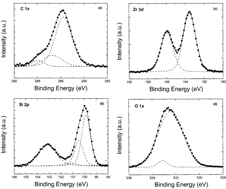
In Fig. 3, the XPS C 1s, Si 2p, and Zr 3d spectra of the films are shown. The C 1s spectrum of Fig. 3a reveals three peaks at 285.79, 286.73, and 287.99 eV, The peak at 285.79 eV is ascribed to C-C or C-H bonds, the peak at 286.73 eV to C-O bonds, and the peak at 287.99 eV to C⫽ O bonds.17No lower binding energy peak char-acteristic of the Zr-C bond was found.18The carbon contamination is due to residual carbon from the precursors and the ambient con-tamination during transfer to the XPS system. After two cycles of sputtering these peaks disappeared, indicating the carbon contami-nation was only on the surface of the films, i.e., the bulk carbon
concentrations were below the limit of our instrument
(⬍0.1 atom %).
In Fig. 3b, the Si 2p peak is fitted with four peaks at 99.9, 100.51, 101.26, and 103.20 eV, respectively. The first two are as-cribed to the Si 2p3/2and Si 2p1/2lines. A spin-orbit splitting con-stant of 0.61 eV and the intensity ratio Si 2p3/2:Si 2p1/2 of 2 was used to fit these peaks. The peak at 101.26 eV is due to an interme-diate oxidation state. The peak at 103.20 eV is 3.3 eV from the Si substrate peak, a chemical shift smaller than the⬎4 eV shift ob-served for 1.8 nm thick SiO2 films.19 This is characteristic of Zr silicate but could also be due to incomplete oxidation of a silicon oxide interfacial layer.
In Fig 3c, the Zr 3d spectrum consists of one doublet with peaks at 183.59 and 185.99 eV, and the expected Zr 3d5/2:Zr 3d3/2intensity ratio of 3/2. This doublet can be ascribed to Si-O-Zr bonds. There is no evidence of Zr-C or Zr-Si bonds in the Zr 3d spectrum.18,20
In Fig. 3d, the O 1s spectrum reveals two peaks at 532.45 and 533.15 eV. The peak at 532.45 eV can be ascribed to the Si-O-Zr bonds. The smaller peak at 533.15 eV is likely associated with the oxynitride layer underneath the silicate film. The binding energy difference Eb(O 1s)⫺ Eb(Zr 3d5/2)⫽ 348.86 eV and Eb(O 1s) ⫺ Eb(Si 2p) ⫽ 429.25 eV are close to the values of 348.35 eV and 429.5 eV, respectively, reported in Ref. 21.
Figure 4 shows the MEIS spectrum for the as-deposited film of Fig. 1a. The solid line is a simulation of the data using the Quark-meis code with a four-layer model共including the substrate whose surface gives rise to a contribution to the Si peak兲. The first layer had the composition CSi0.24O0.36Zr0.07with a total carbon areal den-sity which amounts to approximately 3 monolayers of carbon on the surface of the film. Assuming this layer had the same density as silicon dioxide, it is 0.5 nm thick. The Si, Zr, and O in the top layer are probably due to unreacted or partially reacted precursor mol-ecules. Since the film was maintained in flowing NO at the deposi-tion temperature for several minutes after deposideposi-tion, the amount of undepleted precursor was not expected. Its existence implies that subsequent precursor molecules are involved in the completion of the decomposition reactions of the molecules underneath.
The second layer has the composition Zr0.33Si0.44O2共Si/Zr ratio of 1.3 /1兲. A density for this layer can be estimated by assuming that the molecular volume is the sum of molecular volumes11 of the appropriate amounts of Si, SiO2, and ZrO2. This gives a density of 2.91 gm/cm3and a layer thickness of 1.5 nm.
A layer at the interface was best modeled as 3.3⫻ 1014nitrogen atom/cm2, approximately a half-monolayer of Si atoms on Si共100兲. This is a characteristic of the Si substrate oxidation in nitric oxide at 580°C. Attempts to model the interface layer as an oxynitride or to add another silicon oxide layer on top of the nitrogen layer did not improve the fit. Apparently, the thickness of the interface layer was less than the depth resolution of the MEIS technique, approximately 0.6 nm at the film interface. The total thickness of the three layers determined by MEIS was 2.1 nm, less than the value of 2.6 nm determined by HRTEM and shown in Fig. 1a, but in reasonable
Figure 1. HRTEM cross-sectional images of the as-deposited Zr silicate films deposited in different oxidizing gas at a substrate temperature of 550°C using 12 pulse-mode cycles:共a兲 oxynitride grown at 580°C for 5 min in NO, then Zr silicate deposited with NO,共b兲 oxynitride grown at 580°C for 5 min in NO, then Zr silicate deposited with O2,共c兲 oxide grown at 580°C for 5 min in O2, then Zr silicate deposited with O2, 共d兲 the sample in 共a兲 with spike anneal at 850°C in O2, then the nitrogen anneal at 850°C for 60 s and a FGA at 380°C for 20 min. The Zr silicate layers are 2.0, 1.9, 1.8, and 1.9 nm thick共from a to d兲. The interfacial layers are 0.6, 1.8, 2.4, and 1.4 nm thick共from a to d兲.
Figure 2. AFM image for the film of Fig. 1a. The rms surface roughness is 0.25 nm.
agreement considering the errors in determining thickness from HRTEM micrographs.
The C, N, and O peaks for pieces of the same wafer before and after a spike anneal in O2at 850°C is shown in Fig. 5. The top layer had the composition CSi0.24O0.1.33Zr0.15. and was 0.64 nm thick, assuming it had the density of silicon dioxide. The areal density of carbon decreased, but after annealing, the carbon may have been just adventitious. The Si and Zr in the top layer evidently oxidized. This is corroborated by the oxygen peak in Fig. 5 where the leading edge had shifted to higher energies after oxygen anneal, indicative of some oxide above the Zr silicate layer. The most important change in the MEIS spectra is observed in the broadening of the O peak on the low energy side. The simulation indicates that the interfacial layer increased to a thickness of 0.9 nm and the best fit was obtained assuming that it had the composition SiN0.20O1.73. Attempts to add a zirconium component to this layer did not improve the fit. The thick-ness was again somewhat smaller than the 1.4 nm observed by HR-TEM as shown in Fig. 1d. The fact that the silicon dioxide density resulted in an underestimate of the interfacial layer thickness sug-gests that the interfacial layer was underdense. Given that the
com-Figure 3. XPS spectra with background subtracted showing共䊉䊉䊉兲 data and 共 兲 fitted peaks for the as-deposited Zr silicate film with 12 cycles at
550°C:共a兲 C 1s spectrum with two peaks at 285.79, 286.73 and 287.99 eV, 共b兲 Si 2p spectrum with four peaks at 99.9, 100.51, 101.26, and 103.20 eV, 共c兲 Zr 3d spectrum with two peaks at 183.59 and 185.99 eV, and共d兲 O 1s spectrum with two peaks at 532.45, and 533.15 eV. The solid lines are the sums of the fitted peaks.
Figure 4. MEIS spectrum of 2.7 nm thick as-deposited Zr silicate film with
position is close to that of stoichiometric silicon oxynitride, the magnitude of the discrepancy seems to be much larger than ex-pected. However, errors in determining the thickness of the layers from the HRTEM measurements can be as high as 0.4 nm. The areal density of nitrogen in the interface layer remained constant, to within experimental error, after the spike anneal in O2.
The 100 kHz C-V characteristics共scanned from inversion to ac-cumulation兲 of these films are shown in Fig. 6 for different post deposition annealing共PDA兲 treatments. Each sample was spike an-nealed in O2at 850°C first, followed by subsequent anneals. In Fig. 7, the effect of PDA on the flatband voltage shift (⌬VFB), the fixed charge density (Nf), and the effective density of trapped charge at the interface(⌬Nt) are shown for the samples in Fig. 6. For the film spike annealed in O2 at 850°C, there is a significant hump in the C-V curve. Considering the ideal flatband voltage (VFB⫽ Wms ⯝ ⫺ 0.2 V, where Wmsis the work function difference兲,22the
flat-band voltage VFB⫽ ⫺ 1.01 V corresponds to a positive fixed charge density (Nf⫽ 7.3 ⫻ 1012/cm2). A counterclockwise hyster-esis, with⌬VFB⯝ ⫺ 58 mV, is associated with an effective den-sity of trapped charge at the interface,⌬Nt⫽ 5.2 ⫻ 10
11
/cm2. It is believed that the appearance of the hump is due to Pbcenters at the interface.23,24 For the sample spike annealed in O2 at 850°C and given a subsequent FGA at 380°C for 20 min, the flatband voltage shifted to ⫺0.69 V (Nf⫽ 4.4 ⫻ 1012/cm2) so the hump dimin-ished. The value of⌬VFBis also reduced to⫺26.2 mV, correspond-ing to ⌬Nt⫽ 2.4 ⫻ 1011/cm2. Thus the FGA reduced the charge trapping/detrapping and passivated the Pbcenters effectively.
For the sample spike annealed in O2, then nitrogen annealed at 850°C for 60 s and annealed in forming gas at 380°C for 20 min, the flatband voltage shifted to ⫺0.43 V (Nf⫽ 1.8 ⫻ 1012/cm2). The value of ⌬VFB reduced to ⫺22.5 mV (⌬Nt⫽ 1.9 ⫻ 10
11 /cm2). The N2anneal reduced not only the charge trapping/detrapping but also the leakage current density共shown later兲. For the same sample, negligible hysteresis was observed in the inset of Fig. 7a. In Fig. 7, it is seen that⌬VFB, Nf, and⌬Ntall decreased after the additional nitrogen anneal. The reduction in Nf might have been due to the Figure 5. MEIS C, N, and O peaks for the as-deposited Zr silicate film with
a Si:Zr ratio of 1.3:1 of Fig. 4 before and after spike anneal in O2at 850°C:
共䊉䊉䊉兲 before anneal, 共 兲 simulation, 共䉱䉱䉱兲 after anneal, 共 兲
simulation.
Figure 6. High frequency C-V characteristics of capacitors with Zr silicate
gate dielectric obtained at 100 kHz. The samples were共䊏䊏䊏兲 spike an-nealed in O2at 850°C,共䊉䊉䊉兲 spike annealed in O2at 850°C and FGA at
380°C for 20 min, spike annealed in O2at 850°C, then共䉱䉱䉱兲 annealed in
N2at 850°C for 60 s and FGA at 380°C for 20 min. The EOTs are 2.3, 2.22,
and 2.32 nm, respectively.
Figure 7. The effect of different postdeposition anneals for Zr silicate films
on共a兲 the flatband voltage shift, ⌬VFB,共b兲 the fixed charge density, Nf, and
the effective density of trapped charge at the interface⌬Nt. The spike anneal
was done in O2at 850°C. The FGA is at 380°C for 20 min. The N2anneal
introduction of negative fixed charge and/or the annealing of the positive fixed charge.
Figure 8 shows the 10 kHz, 100 kHz, and 1 MHz C-V curves of the Zr silicate film spike annealed at 850°C in O2, then nitrogen annealed at 850°C for 60 s and annealed in forming gas at 380°C for 20 min. The area of the capacitor is 2.8⫻ 10⫺4 cm2. From the 100 kHz C-V curve, the EOT is 2.32 nm with the quantum correction. Compared with the frequency dispersion of the sample spike an-nealed in O2at 850°C and then given a FGA at 380°C for 20 min 共shown in the inset of Fig. 8兲, there is only a small frequency dis-persion in the C-V curves due to interface states, mainly below the midgap. This indicates that most of the interface states, not passi-vated by the FGA, were eliminated by the nitrogen anneal at 850°C for 60 s. The slight dispersion due to the remaining interface states might be further reduced with a postmetallization anneal because the reaction between the metal and residual water on the surface can generate atomic hydrogen which is more effective in passivating interface states than molecular hydrogen.25
For the as-deposited and spike annealed samples of Fig. 8, electron-energy-loss spectroscopy 共EELS兲 spectra confirmed the conclusion from the MEIS spectra that the Zr content in the interfa-cial layer was below the detection limit.26 Assuming a dielectric constant appropriate for SiO2 of 3.9 for the interfacial layer, a di-electric constant of 8.5 was determined for the Zr silicate layer.
Figure 9 shows the corresponding leakage current densities as a function of gate voltage for the samples in Fig. 6 under substrate injection共positive gate voltage兲. The leakage current of the film is reduced by orders of magnitude after the spike anneal in O2. Some of the reduction of leakage current is due to the increase of the EOT associated with the increase in interfacial layer thickness noted in the Fig. 9 and the rest may be due to the decrease of traps which contribute to trap-assisted tunnelling current.27 The small change observed after the FGA may be due to variations in film thickness over the wafer. A further significant current decrease in leakage current is noted after nitrogen annealing, probably related to a fur-ther decrease in trap-assissted tunnelling. For the annealed samples, the J-V curves are similar to those associated with soft breakdown in SiO2films and are characteristic of the trap-assisted tunnelling in the Zr silicate films.27,28
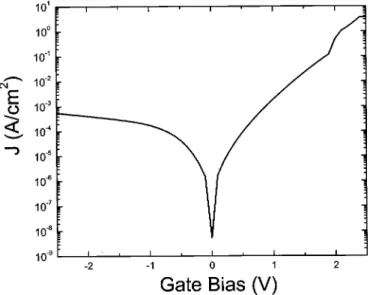
In Fig. 10, the leakage current densities as a function of gate bias under substrate and gate injection are shown, indicating the polarity dependence. The leakage current density at VG-VFB⫽ 1 V is 1.4 ⫻ 10⫺4 A/cm2, which is about 20 times lower than that of SiO
2 with the same EOT (3⫻ 10⫺3 A/cm2).29The leakage was higher under substrate injection than under gate injection. The tunnelling probability is inversely proportional to the tunnelling area defined by the electron tunnelling distance and the barrier height. Under gate injection, the tunnelling area was larger, i.e., the electron tunnelling probability is lower as described in Ref. 30, thus the leakage current is lower for gate injection.
Conclusions
In this study, ultrathin Zr silicate films were deposited on Si共100兲 using Zr(Oi-Pr)2(thd)2 and Si(Ot-Bu)2(thd)2 dissolved in octane. Either O2or NO was used as the oxidizing gas. Nitric oxide forms Figure 8. Frequency dependence of the C-V characteristics of the Zr silicate
film which has an EOT of 2.32 nm after a spike anneal at 850°C in O2,
followed by a nitrogen anneal at 850°C for 60 s and a FGA at 380°C for 20
min:共䊏䊏䊏兲 10 kHz, 共䊉䊉䊉兲 100 kHz, and 共䉱䉱䉱兲 1 MHz. A slight
fre-quency dispersion is evident below midgap, indicating the existence of donor-like interface states. The inset shows the frequency dispersion of the sample after a spike anneal at 850°C in O2and a FGA at 380°C for 20 min.
Figure 9. Current density as a function of gate voltage for the Zr silicate
film of Fig. 6 with for substrate injection: 共䉱䉱䉱兲 as-deposited, after
共⽧⽧⽧兲 a spike anneal at 850°C in O2and a FGA at 380°C for 20 min, after 共夝夝夝兲 only a spike anneal at 850°C in O2, after共䊏䊏䊏兲 a spike anneal at
850°C in O2, followed by a nitrogen anneal at 850°C for 60 s and a FGA at
380°C for 20 min.
Figure 10. Current density as a function of gate voltage for the sample in
an oxynitride buffer layer which retards oxygen diffusion to the Si interface. Both NO and O2reduce the carbon contamination effec-tively. No evidence of C-Si, Zr-C and Zr-Si bonds were found in the XPS spectra. HRTEM images showed that the as-deposited Zr silicate films were amorphous. After postdeposition anneals at 850°C, Zr silicate films with the composition Si:Zr ratio of 1.3:1 were still amorphous and no phase separation was observed.
The HRTEM images and MEIS analysis showed that a substan-tial interface layer, 0.9-1.4 nm thick, was produced by a spike anneal in O2 at 850°C. The Zr concentration in the interfacial layer was below the sensitivity of the MEIS technique (⬃5 atom %) after annealing and this has been confirmed by EELS analysis. Limiting the growth of the interface layer will require a reduction in the thermal budget during any O2 anneal, and this needs to be further investigated.
One of the functions of the O2 anneal was to eliminate the C from precursor evidently left on the surface of the film. The fact that this remaining precursor was not oxidized during the final oxidation stage in the deposition chamber suggests that the decomposition of the precursor is a rather complicated process requiring both a sepa-rate oxidant and species produced during the succeeding precursor pulse.
The ultrathin Zr silicate films described in this work exhibit promising C-V and J-V characteristics. The Pbcenters at the inter-face were effectively passivated by FGA, consistent with the hy-pothesis that the interfacial layer was silicon oxide. The hysteresis, fixed charge density, and the effective density of trapped charge at the interface are also improved significantly by anneals at 850°C. Most of the frequency-dependent interface states, not passivated by the low temperature FGA, were eliminated after the 60 s nitrogen anneal at 850°C. The slight remnant frequency dispersion below midgap might be reduced if a proper FGA were performed after, rather than before, gate electrode definition. Higher temperature an-nealing might also reduce the remnant dispersion but the films may crystallize at temperatures above 900°C. After a spike anneal in O2 at 850°C and an anneal for 60 s in N2at 850°C, a Zr silicate film with an EOT of 2.32 nm exhibited a leakage current about 20 times lower than that of a SiO2film with the same EOT. These electrical properties demonstrate that a thin Zr silicate film formed by Zr(Oi-Pr)
2(thd)2, Si(Ot-Bu)2(thd)2 and nitric oxidemight be a promising gate dielectric for deep submicron CMOS devices, if ways can be found to decrease the interface layer thickness.
Acknowledgments
The authors are grateful to X. Tong and T. Quance for assistance in the preparation of the samples. In addition, we wish to thank Dr. J. R. Hauser for use of the NCSU C-V analysis program. This work was supported by the National Science Council of the Republic of China under contract no. NSC90-2215-E-009-117.
National Chiao-Tung University assisted in meeting the publication costs of this article.
References
1. S.-H. Lo, D. A. Buchanan, Y. Taur, and W. Wang, IEEE Electron Device Lett., 18, 209共1997兲.
2. G. D. Wilk, R. M. Wallace, and J. M. Anthony, J. Appl. Phys., 89, 5243共2001兲. 3. D. J. Hubbard and D. G. Schlom, J. Mater. Res., 11, 2757共1996兲.
4. J. Robertson, J. Vac. Sci. Technol. B, 18, 1785共2000兲.
5. W.-J. Qi, R. Nieh, B. H. Lee, K. Onishi, L. Kang, Y. Jeon, J. C. Lee, V. Kaushik, B. Y. Nguyen, L. Prabhu, K. Eisenbeiser, and J. Finder, Technical Digest for VLSI Symposium, p. 40共2000兲.
6. A. C. Jones, Chem. Vap. Deposition, 4, 169共1998兲.
7. S. B. Desu, T. Shi, and C. K. Kwok, Mater. Res. Soc. Symp. Proc., 168, 349共1990兲. 8. A. C. Jones, T. J. Leedham, P. J. Wright, M. J. Crosbie, P. A. Lane, D. J. Williams, K. A. Fleeting, D. J. Otway, and P. O’Brien, Chem. Vap. Deposition, 4, 46共1998兲. 9. H.-W. Chen, T.-Y. Huang, D. Landheer, X. Wu, S. Moisa, G. I. Sproule, and T.-S.
Chao, J. Electrochem. Soc., 149, F49共2002兲.
10. B. C. Hendrix, A. S. Borovik, Z. Wang, C. Xu, J. F. Roeder, T. H. Baum, M. J. Bevan, M. R. Visokay, J. J. Chambers, A. L. P. Rotondaro, H. Bu, and L. Colombo, Mater. Res. Soc. Symp. Proc., 716, B6.7.1共2002兲.
11. H.-W. Chen, D. Landheer, T.-S. Chao, J. E. Hulse, and T.-Y. Huang, J. Electro-chem. Soc., 148, F140共2001兲.
12. CRC Handbook of Chemistry and Physics, Chemical Rubber Corp., Boca Raton, FL共1983兲.
13. QUARKMEIS, simulation program, www.quarksimulation.com
14. J. B. Marion and F. C. Young, Nuclear Reaction Analysis: Graphs and Tables, p. 36, North-Holland Publishing Co., Amsterdam共1968兲.
15. G. Lucovsky and G. B. Rayner, Jr., Appl. Phys. Lett., 79, 4195共2001兲. 16. J. R. Hauser and K. Ahmed, in Characterization and Metrology for ULSI
Technol-ogy:1998 International Conference, D. G. Seiler, A. C. Diebold, W. M. Bullis, T. J. Shaffner, R. McDonald, and E. J. Walters, Editors, p. 235, The American Institute of Physics, Woodbury, NY共1998兲.
17. B. Cho, S. Lao, L. Sha, and J. P. Chang, J. Vac. Sci. Technol. A, 19, 2751共2001兲. 18. S. Kato, K. Ozawa, K. Edamoto, and S. Otani, Jpn. J. Appl. Phys., Part 1, 9, 5217
共2000兲.
19. S. Iwata and A. Akitoshi, J. Appl. Phys., 79, 6658共1996兲.
20. G. D. Wilk, R. M. Wallace, and J. M. Anthony, J. Appl. Phys., 87, 484共2000兲. 21. J. Guittet, J. P. Crocombette, and M. Gautier-Soyer, Phys. Rev. B, 63, 125117
共2001兲.
22. E. H. Nicollian and J. R. Brews, MOS (Metal Oxide Semiconductor) Physics and Technology, Wiley, New York共1982兲.
23. P. Lundgren and M. O. Andersson, J. Appl. Phys., 74, 4780共1993兲. 24. A. Stesmans and V. V. Afanas’ev, Appl. Phys. Lett., 80, 1957共2002兲.
25. P. Balk, Abstract III, The Electrochemical Society Extended Abstracts, Buffalo, NY, Oct 10-14, 1965; B. E. Deal, E. L. MacKenna, and P. L. Castro, J. Electro-chem. Soc., 116, 997共1968兲.
26. X. Wu, D. Landheer, and H.-W. Chen, Unpublished work.
27. M. Depas, T. Nigam, and M. Heyns, IEEE Trans. Electron Devices, 43, 1499
共1996兲.
28. M. Houssa, M. Tuominen, M. Naili, V. V. Afanas’ev, A. Stesmans, S. Haukka, and M. M. Heyns, J. Appl. Phys., 87, 8615共2000兲.
29. B. Brar, G. D. Wilk, and A. C. Seabaugh, Appl. Phys. Lett., 69, 2728共1996兲. 30. M. Houssa, M. Naili, V. V. Afanas’ev, M. M. Heyns, and A. Stesmans, in
Proceed-ings of the 2001 International Symposium on VLSI Technology, Systems, and Ap-plications, IEEE p. 196共2001兲.