Propagation of surface acoustic waves through sharply bent two-dimensional phononic crystal
waveguides using a finite-difference time-domain method
Jia-Hong Sun and Tsung-Tsong Wu*
Ultrasonics Lab., Institute of Applied Mechanics, National Taiwan University, Taipei 106, Taiwan
共Received 26 June 2006; revised manuscript received 1 September 2006; published 30 November 2006兲
In this paper, we adopt the finite-difference time-domain共FDTD兲 method to analyze surface acoustic waves propagating in two-dimensional phononic waveguides. To implement the FDTD program for dealing with surface acoustic waves, the Bloch theorem and absorbing boundary conditions are employed to deal with the periodic boundary condition and reflection from a numerical boundary. A phononic crystal consisting of circular steel cylinders that form a square lattice in an epoxy matrix is considered as an example to study phononic crystal waveguides. The dispersion relation and displacement fields are calculated to identify the band gaps and eigenmodes. The result shows the existence of a complete band gap of surface waves and thus an acoustic waveguide is created accordingly. Eigenmodes of surface waves inside the waveguide are indicated and pseudo surface acoustic waves propagating inside the straight waveguide are demonstrated. Further, waveguides with a sharp bend are reported and an improved design is suggested to enhance energy transmission.
DOI:10.1103/PhysRevB.74.174305 PACS number共s兲: 63.20.⫺e, 43.20.⫹g, 43.40.⫹s, 46.40.Cd
I. INTRODUCTION
Phononic crystals consisting of periodic elastic materials have been proved to have a property of band gaps. In various phononic crystals, both the bulk acoustic wave 共BAW兲1–3 and surface acoustic wave共SAW兲4–8are analyzed, and com-plete band gaps, the frequency range that acoustic waves cannot propagate in any direction, were observed in some cases. The complete band gap phenomenon plays an impor-tant role in designing phononic crystal applications such as elastic wave filters, couplers, and waveguides, especially. The phononic crystal waveguide is an important elementary component to build an acoustic wave circuit. Currently, most of the phononic waveguide researches are focused on the bulk acoustic waves. The presented BAW waveguides are consisted of solid/solid,9–11solid/liquid,12,13and gas/liquid12 phononic crystals. The designs include straight waveguides with various widths,10 waveguides with a stub,12 a wave-guide with hollow cylinders,13and a coupler of joined paral-lel waveguides.11In contrast, the study of SAW in phononic crystal has had less progress. Laude et al.8 reported a com-plete band gap of surface acoustic wave in a piezoelectric phononic crystal; Tanaka and Tamura14analyzed the surface and surface-guided waves in phononic lattices. More inves-tigations on the surface waves in phononic waveguides are awaited.
In this paper, we study the surface wave propagation in phononic waveguides. To accomplish this work, a FDTD method is developed to analyze the dispersion of acoustic wave in phononic crystals. The Bloch theorem and a per-fectly matched layer 共PML兲 absorbing boundary condition are employed to deal with the periodic boundary condition and numerical nonreflection boundary respectively.15A steel/ epoxy square lattice phononic crystal is studied and the com-plete band gap of the surface acoustic wave is obtained. With the complete band gap property, a phononic waveguide for surface waves is designed by arranging adjacent point de-fects. Thus, eigenmodes of surface waves inside the
wave-guide are indicated and surface acoustic waves propagating inside the straight waveguide are demonstrated. The result shows that the allowed surface waves can propagate and are confined within the waveguide. Further, the waveguides with a sharp bend are reported and an improved design is sug-gested to enhance energy transmission.
II. FINITE-DIFFERENCE TIME-DOMAIN METHOD In a linear elastic material, the equation of motion and constitutive law of elastic materials can be expressed as
u¨i=ij,j+fi, 共1兲
ij= Cijklkl, 共2兲
where is the density of materials, ui the displacement,ij
the stress, fibody force, Cijklelastic constant, andklstrain.
Equations共1兲 and 共2兲 describe the property of an infinitesi-mal element of an anisotropic material in general. These equations are applicable to the inhomogeneous structure of phononic crystals by arranging the density and elastic con-stant periodically. Further, with staggered grids, differential equations共1兲 and 共2兲 are transferred into difference equations based on the Taylor’s expansion to develop the three-dimensional heterogeneous finite difference formulation. Then these equations are calculated recursively, indefinitely, to study the wave propagation in phononic crystals.
The Bloch’s theorem is introduced to treat the periodic boundary condition of a unit cell of phononic crystals. The displacement and stress fields of phononic crystals can be expressed by a plane wave and a periodic function as
ui共x,t兲 = eik·xUi共x,t兲, 共3兲
ij共x,t兲 = eik·xTij共x,t兲, 共4兲
where k is a wave vector. Ui共x,t兲 and Tij共x,t兲 are periodic
ij共x + a,t兲 = eik·aij共x,t兲. 共8兲
With the PBC, both the two-dimensional共2D兲 and three-dimensional共3D兲 phononic crystal cases can be analyzed by calculating a unit cell. In the analyses of dispersions, a small disturbance in a random position of the unit cell is set as the initial condition. Thus, all possible wave modes are trans-ported inside the considered phononic crystal, and the dis-placement is recorded and expanded into Fourier series. Then the eigenfrequencies of a given wave vector k are in-dicated by selecting the resonance peaks of the spectrum, and this allows us to find the information about possible types of bulk waves.
To solve the surface acoustic wave modes of phononic crystals, extra boundary conditions are needed to develop surface acoustic waves inside a phononic crystal unit cell. In this study, we set a free surface boundary condition and use the PML absorbing boundary condition to deal with the re-flection from the numerical boundary.
Berenger18 introduced the concept of PML to reduce the electromagnetic wave reflection form boundary, and the PML is also developed to calculate the elastic wave propagation.19,20 In this paper, a 3D PML program of or-thogonal material is adopted to serve the nonreflection boundary condition. A stretched coordinate is defined with a complex variable,
ei= ai+ i
⍀i
, 共9兲
to derive the code of PML region.19In Eq.共9兲, the real part
aiis the scale factor, and⍀i/is the imaginary part with the
attenuation factor⍀iand the circular frequency. Then the
differential operation in the stretched coordinate is defined and applied to the equation of motion and constitutive law. After introducing the plane wave solutions into the equa-tions, the numerical attenuation is achieved via the factor⍀i.
In addition, a nonreflection condition at the interface be-tween PML region and inner space is obtained by setting corresponding material constants and the unity scale factor. In the elastodynamic equations for the stretched coordinate, displacement and stress components are taken spatial partial differential operation in all directions, thus the variables are split into three components to realize the difference equa-tions. Then actual values are obtained from the summation of splitting components. Finally, the PML equations can be shown, as follows:
rapidly inside the region. With this absorbing boundary con-dition, the reflection is reduced to less than 1% and the PML boundary is used in both the calculations of dispersion rela-tion and transmission.
III. COMPLETE BAND GAPS OF STEEL/EPOXY PHONONIC CRYSTALS
To investigate the band gap of phononic crystal, the dis-persion relation of elastic waves inside phononic crystals is calculated first. In this paper, a square lattice phononic crys-tal consisting of steel cylinders embedded in an epoxy half space is analyzed to demonstrate the band gap of surface acoustic wave. The lattice constant a of the phononic crystal is 8 mm and the radius r of steel cylinder is 3 mm, and thus the filling ratio f defined as r2/ a2 is equal to 0.442. The
density and elastic constant C11and C44of steel are assumed as 7900 kg/ m3, 280.2 GPa, and 82.9 GPa, respectively, and those for epoxy are 1180 kg/ m3, 7.61 GPa, and 1.59 GPa. Thus the impedance of cylinders is more than 15 times the one of the matrix.
In 2D phononic crystal cases, the surface acoustic wave propagates within the x-y plane perpendicular to the cylin-ders. However, the surface acoustic wave is indeed a 3D problem in the phononic crystals. We defined a 3D unit cell as shown in Fig.1共a兲to calculate the characteristic mode of surface acoustic waves. The dimension of this unit cell is chosen as 1a⫻1a of the cross section on the x-y plane and the height h is 9a to develop surface acoustic waves. Then a free surface boundary is on the surface at z = 0, and a 20-layer PML region is under the bottom surface to apply the nonreflection boundary. Finally, the PBC is defined on the other four surfaces of the unit cell. In the FDTD method, each unit cell is divided into 24⫻24 grids and a time step interval is 20 ns to satisfy the numerical stability conditions. To calculate dispersion curves of acoustic waves, the first Brillouin zone of the square array phononic crystal is shown in Fig. 1共b兲. The right-angle isosceles triangle refers to the smallest nonreducible area of this phononic crystal, and the vertexes of triangle are denoted as⌫, X, and M, respectively. Similar to the process in calculating the bulk acoustic waves, an initial condition is set and the displacement is recorded and transferred into Fourier series. The eigenmodes are ob-tained by selecting the resonance peaks on the power spectra. By varying the wave vector k and repeating the calculation, the dispersion curve is obtained.
In a 2D phononic crystal, the structure is infinite along the
z direction. Thus bulk acoustic waves propagate within the x-y plane perpendicular to the cylinders, and the polarization
modes are decoupled as the in-plane mode 共x-y plane兲 and the antiplane mode. In Fig.2, the eigenmodes of bulk acous-tic waves are presented in solid and hollow circles for in-plane and antiin-plane modes respectively. In the in-in-plane modes, there is a noticeable wide complete band gap from 90 to 204 kHz and several narrow complete band gaps at higher range 231– 237 kHz and 245– 255 kHz. From the curves of antiplane modes, band gaps locate at 55–143, 153– 212, 225–250, and 270– 276 kHz. Considering both modes together, the complete band gaps are at 90–143, 153–204, 231–237, and 245– 250 kHz.
Using the 3D unit cell with PBC, free surface, and PML, the eigenmodes are obtained and marked as rhombus sym-bols in Fig. 2. As shown in the figure, extra modes are de-tected by the sensors on the free surface. For example, dif-ferent bands appear at 7 – 79.5 kHz and 199– 201 kHz in the ⌫X direction. Also, some selected peaks overlap the circle
symbol of BAW modes, such as the first and second bands of in-plane and antiplane transverse waves in the⌫X direction. In the higher frequency range, there are numerous peaks, but most peak values are very small.
To investigate the modes of acoustic wave detected in the 3D phononic crystal unit cell, the displacement distributions of the eigenmodes are calculated. The calculating setup is the same as Fig. 1共a兲 but the initial condition is replaced by a wave source. The source generates a wave package of chosen frequency that is the same as the eigenfrequency of the cor-responding wave vector. Because both the wave vector and frequency are assigned, the specific eigenmode is excited and the displacement field is recorded to help identify the prop-erties of modes. The displacement distributions of the eigen-modes are plotted in a 3D vector plot. In Fig. 3 and the following 3D vector figures, the direction of cones is used to indicate the direction of displacement vector and the size reflect the magnitude of vectors. The color of cones changes with the z-axis coordinate of particles to help easily distin-guish the location. Besides, the unit cell has grid lines in the location of multiples of the lattice constant.
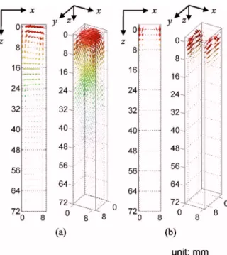
First, two eigenmodes that differ from those of BAW are calculated. The eigenmodes of wave vector k =共/ a , 0兲 with frequency f = 77 kHz 共point A in Fig. 2兲 and f =199 kHz 共point B in Fig.2兲 are shown in Figs. 3共a兲and3共b兲. These modes of wave vector k =共/ a , 0兲 propagate along the x di-rection in Fig. 3. The wavelength of the first band with 兩k兩 =/ a is 2a and thus only a half of the periodic displacement field is shown is one unit cell. The wave in Fig.3共a兲has a main polarization in the sagittal plane, the x-z plane, and the wave in Fig. 3共b兲 has a main polarization in the x-y plane. The result shows confined displacement fields; the amplitude decays rapidly as the depth increases. Thus, they present a typical property of surface acoustic wave. An interesting
FIG. 1. 共Color online兲 The phononic crystal with circular rods 共steel兲 embedded in a background material 共epoxy兲 arranged in square lattice.共a兲 The 3D unit cell of phononic crystal employed to calculate surface acoustic waves;共b兲 the first Brillouin zone of a square lattice crystal.
FIG. 2. 共Color online兲 Dispersion of eigenmodes in the square lattice steel/epoxy phononic crystal.
FIG. 3. 共Color online兲 The 3D displacement fields of eigen-modes. 共a兲 k=共/a,0兲, f =77 kHz 共point A of Fig. 2兲; 共b兲 k
field that remains within the depth of the unit cell. Thus, the peaks overlapped on the modes of BAW present the property of BAW.
The analysis shows that the 2D steel/epoxy square phononic crystal with a free surface allows PSAW instead of SAW. The dispersion curves show an important fact that there exists a complete band gap of both BAW and PSAW 共SAW兲 in this phononic crystal. The complete band gaps obtained by both results of 2D and 3D unit cell locate from 90– 143 kHz and 154– 199 kHz. This is the basis on which to design a phononic crystal waveguide of surface waves.
In brief, some properties of using FDTD method in cal-culating eigenmodes can be drawn. In the lower frequency range of the first band, the acoustic wave has a long wave-length. Thus some PSAW 共or SAW兲 do not develop well because of the finite depth of the unit cell and the absorbing boundary condition. Also, in the case of energy leakage sur-face waves, the characteristic displacement decays rapidly, and thus sometimes the sensor on the free surface may be insensitive and miss the leakage modes. Second, in the dis-persion curves, some eigenmodes calculated from the FDTD program of 3D condition repeat the result from the 2D BAW conditions. Finally, the natural property of FDTD limits the accuracy of result in high-frequency range. Even with imper-fections, the FDTD method is a powerful tool to calculate and analyze the eigenmodes, and the accuracy can be raised by increasing the sampling grid size with the improvement of computers.
IV. SURFACE ACOUSTIC WAVES INSIDE A PHONONIC CRYSTAL WAVEGUIDE
A phononic crystal waveguide is designed by arranging adjacent point defects in a phononic crystal structure. These defects form a continuous region that is free of inclusions and in which acoustic waves are expected to propagate. Cur-rently, most studies focus on BAW in phononic crystal waveguides9–13 and the analysis of SAW in waveguides is just started.14 In this section, the FDTD method is used to calculate surface acoustic wave propagation inside a phononic waveguide and, further, the bending waveguides are analyzed.
A phononic crystal waveguide of surface acoustic waves is formed based on the complete band gap of surface waves. The acoustic waves in the waveguide cannot penetrate the periodic structure and thus other eigenmodes 共the guided
modes兲 result from the existence of defects that appeared at the range of complete band gaps. In the steel/epoxy phononic crystal presented in Sec. III, the complete band gaps are 90– 143 and 154– 199 kHz.
To understand the property of SAW inside phononic crys-tal waveguides, the supercell technique is used to analyze the dispersion of a waveguide. We consider a waveguide with a 10 mm width w共the distance between two neighboring cyl-inders on both sides兲 as shown in Fig. 4. A 3D supercell consisting of 11⫻1⫻9 unit cells is defined, and then the waveguide is constructed of ten periodic arrayed cylinders and a dislocation in the center with the PBC surrounding it. Similarly, an initial disturbance is defined inside the wave-guide, and thus acoustic waves are generated and the dis-placement field is recorded. Then the eigenmodes are se-lected from the local maximum peaks of spectra as the procedure of analyzing a unit cell. By setting corresponding boundaries, both the dispersion calculated by 2D and 3D supercells are obtained and plotted in Fig. 5. Figure 5 is focused on the frequency of 70– 220 kHz to observe defect modes in the range of complete band gaps. The extended bands outside the complete band gaps are omitted and the region is marked in gray. As shown in the result, other defect modes of acoustic waves appear in the range of complete band gaps. The eigenmodes of BAW are marked as solid and hollow circles and those obtained from the 3D supercell are rhombus symbols.
The defect modes of BAW are similar to the result of a previous study,10and there are different defect modes result-ing from the free surface and nonreflection condition in the dispersion diagram. In the 3D supercell, sensors on the free surface of phononic crystal waveguide receive the signal of defect modes of both BAW and SAW. The signal of BAW modes has a small peak value and make the spectrum show a complex pattern. Thus, in the 3D waveguide calculation, the BAW modes are removed and only the SAW mode is shown in Fig.5. Inside the first complete band gap of 90– 143 kHz, a band extends from wave vector k =共/ a , 0兲 with frequency
f = 87.5 kHz to k =共0.05/ a , 0兲 with f =141 kHz, and
an-other band appears from k =共0.75/ a , 0兲 with f =154 kHz to k =共0.9/ a , 0兲 with f =206 kHz in the second complete band gap of 154– 199 kHz.
The displacement fields of the two defect modes are plot-ted in 3D vector diagrams as those in Fig.3. The eigenmodes
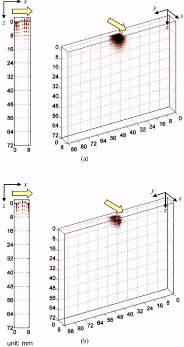
of k =共0.5/ a , 0兲 with f =114.5 kHz 共point A in Fig.5兲 and k =共0.5/ a , 0兲 with f =180 kHz 共point B in Fig. 5兲 are cal-culated and shown in Figs.6共a兲and6共b兲, respectively. Since the dispersion diagram is presented in a reduced zone scheme, the actual wave vectors of these two modes in folded bands are k =共1.5/ a , 0兲 and k=共2.5/ a , 0兲 with wavelengths of 1.33a and 0.8a, and the consistent result is obtained from the displacement fields of x-z plane. The guided waves propagate along the x direction, and the dis-placement fields have a confined distribution within the re-gion of waveguides. The maximum amplitude occurs on the free surface and the amplitude decays rapidly in a deeper location. Thus these two bands have a typical property of surface acoustic waves.
A further discussion of the defect modes in phononic crystal waveguide is presented as follows. In the calculation of eigenmode displacement fields, a Gaussian weighted wave package with specified frequency f is set as the source and input finite energy into the supercell structure to excite the selected eigenmode. Then, the sensor on the free surface de-tects a monotonous displacement variation and the vertical component Uz recorded after the wave package is excited. The result shows that the eigenmode has decaying amplitude. This means an energy leakage, partial acoustic waves propa-gate downward into the half space, and thus the defect modes in this phononic crystal waveguide are actual pseudo surface acoustic waves. Finally, converting the period of signal into propagation distance, the attenuation coefficient is obtained as −0.049dB/ a and −0.061dB/ a for these eigenmodes re-spectively.
To demonstrate the actual wave propagation inside the phononic crystal waveguide, the linear waveguide consid-ered shown in Fig.7. As a 3D structure, Fig.7 shows a top view of the free surface and the actual structure extends to-ward vertically to the surface. The periodic circles present the boundaries of steel cylinders and the epoxy matrix. The waveguide has a width of 10 mm by removing one row of adjoining cylinder inclusions along the⌫X-direction, and the length of waveguide is 25a. An acoustic wave is generated in the inlet of waveguide with five line sources to simulate an interdigital transducer 共IDT兲. The PSAW defect mode of wavelength=1.33a with frequency f =114.5 kHz is gener-ated and the wave propagation pattern is demonstrgener-ated. The displacement field of the z-direction component Uz is
pre-FIG. 5. 共Color online兲 Dispersion diagram of BAW and SAW eigenmodes in the steel/epoxy phononic crystal waveguide with a free surface.
FIG. 6. 共Color online兲 The 3D displacement fields of defect modes inside the phononic crystal waveguide.共a兲 k=共0.5/a,0兲,
f = 114.5 kHz共point A of Fig. 5兲; 共b兲 k=共0.5/a,0兲, f =180 kHz
sented in grayscale to show the surface wave propagation. The black is the minimum共negative兲 value and the white is the maximum共positive兲 value. The scale is fixed in this pa-per for the convenience to compare the amplitude in different cases. The result shows that the PSAW is confined well within the waveguide and only slight energy leaks into the periodic phononic crystal area. In addition, although the PSAW has energy leakage, the PSAW propagates along the waveguide and carries most energy.
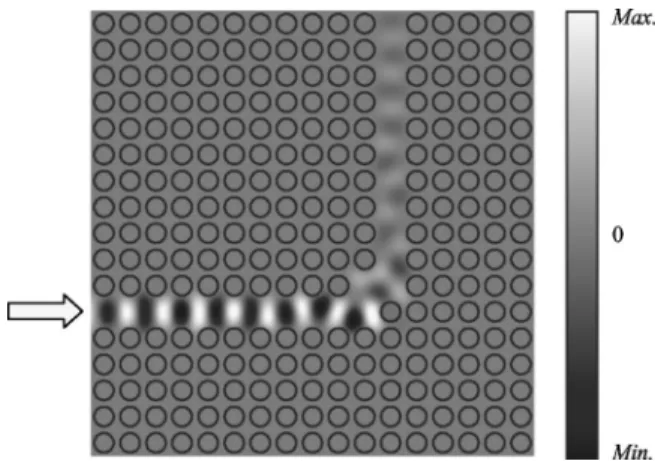
In acoustic waveguides, a bend section is an elementary structure to change the wave propagation direction. Here the phononic crystal waveguide with a sharp bend is also calcu-lated to estimate the transmission efficiency. The first case is a simple junction of two ⌫X-direction waveguides. The structure is a 17a⫻17a area and two 11a waveguides are connected as shown in Fig.8. The same PSAW of 114.5 kHz defect mode is launched into the waveguide from the inlet in the lower-left corner and the Uz displacement field on the surface is shown in the same grayscale. The displacement pattern shows that PASW is still confined within the bending waveguide structure, but most energy of the incident wave is reflected at the corner of the bend. In the case of a linear straight waveguide in Fig. 7, the 114.5 kHz PSAW in the outlet has an amplitude of 2.9⫻10−14m as a reference value
that results from a monotonous body force of 1 nt/ kg peak value as a wave source. With the identical wave source, the maximum amplitude on the surface of the vertical waveguide branch is about 1.7⫻10−14m 共59% of the reference
ampli-tude兲 in the bending waveguide. Another phenomenon is that BAW modes are also excited as the wave turns, and thus
considerable energy is taken away and the amplitude in the vertical branch decays rapidly. Thus, a simple joint bend is not an efficient design.
Another bend structure is shown in Fig.9. It contains two linear waveguides in the ⌫X-direction and one in the ⌫M-direction; thus, the wave turns 45° twice to the left di-rection. The Uz displacement pattern of 114.5 kHz PSAW defect mode also shows a strong reflection of the incident wave. The amplitude of the turned wave is about 1.5 ⫻10−14m 共52% of the reference amplitude兲 in the
⌫M-direction segment and 0.75⫻10−14m共26%兲 in the
ver-tical⌫X-direction segment. Finally, the mode of the turned wave is rebuilt to a symmetric PSAW mode. In these cases, the wavelengths of PSAW are almost the same with a lattice constant, and thus there is a strong scattering phenomenon when acoustic waves encounter inclusions at their propagat-ing direction. In addition, the antisymmetry conjunction sec-tion in Fig. 9 also enhances the scattering and the mode conversion. Therefore, energy disperses while the excited BAW propagates downward, and thus the surface amplitude decays when the PSAW encounters the boundary of the bending waveguides.
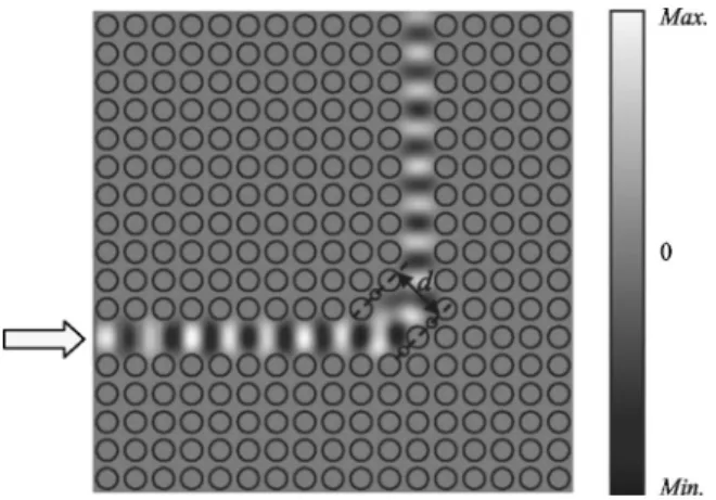
To raise the transmission of the bending phononic crystal waveguide, an improved bend structure is introduced. In the study of photonic crystals, the scatters are used to enhance transmission through waveguide bends in two-dimensional photonic crystal slabs.21,22 The idea is adopted in this paper to raise the transmission of PSAW in phononic crystal waveguides. The design is based on the prototype shown in Fig. 9 and the cylinders of smaller radius 1.3 mm are in-serted into the⌫M-direction segment. With the inserted scat-ters, the conjunction section has a better symmetric geometry property. This also changes the dispersion curve, compared to the result shown in the photonic crystal cases, and results in eigenmodes that propagate in the conjunction section with less loss. In Fig. 10, the distance d between the center of scatters is 16.97 mm 共3
冑
2a / 2兲. Then the Uz displacement pattern of PSAW of 114.5 kHz is calculated and shown. Ob-viously, the PSAW passing the corner remains the same eigenmode and therefore the amplitude is raised to 2.1 ⫻10−14m共72% of the reference amplitude兲.Further calculation shows that the transmission of the guided PSAW is affected by the scatters obviously. If the
FIG. 8. The z-direction displacement field of the 114.5 kHz PSAW inside a sharp bending waveguide.
FIG. 9. The z-direction displacement field of the 114.5 kHz PSAW inside a three-segment bending waveguide.
scatters are moved toward the center of the waveguide, the dispersion relation is altered. In the case of the distance d of 11.31 mm 共
冑
2a兲, the amplitude of turned-PSAW at 114.5 kHz becomes 1.4⫻10−14m共48% of the referenceam-plitude兲. Another important fact is that waves of different frequency in the structure do not have identical perfor-mances. The PSAW of 135 kHz in the bend structure of Fig. 10shifts to BAW mode and the mode decays very rapidly in the turned waveguide, but has a 1.8⫻10−14m共62%兲
ampli-tude ratio in the structure with d of 11.31 mm. Therefore, the transmission efficiency is affected by the scatters and also a function of frequency. Indeed, setting scatters properly in the
phononic crystal waveguides can raise the transmission and change the propagation direction in a small region.
V. CONCLUSION
In this paper, we implement a FDTD method to analyze propagation of surface acoustic wave inside phononic crystal waveguides. Combing the free surface, PBC, and PML con-ditions, the eigenmodes of the 2D phononic crystals with a free surface is calculated in detail. The steel/epoxy phononic crystal shows a complete band gap for both bulk and surface acoustic waves. Further, phononic crystal waveguides are de-signed based on the complete band gap phenomenon. We found that the defect mode inside the phononic crystal wave-guide has an energy leakage because the 3D structure allows the wave propagating downward to the half space. The eigenmodes of the 2D phononic crystal waveguide with a free surface is thus identified as PSAW. Although the PSAW has a slight energy leakage inside the 2D waveguide, it is possible to have a waveguide with a sharp bend. Adding scatters inside the phononic crystal waveguides can raise the transmission and the design depends on the frequency of PSAW.
ACKNOWLEDGMENT
The authors gratefully acknowledge the financial support of this research by the National Science Council, Taiwan 共Contract No. NSC 94-2212-E-002-040兲.
*Corresponding author. Email address: [email protected]
1M. S. Kushwaha, P. Halevi, L. Dobrzynski, and B.
Djafari-Rouhani, Phys. Rev. Lett. 71, 2022共1993兲.
2M. S. Kushwaha, P. Halevi, G. Martinez, L. Dobrzynski, and B.
Djafari-Rouhani, Phys. Rev. B 49, 2313共1994兲.
3M. S. Kushwaha and P. Halevi, Appl. Phys. Lett. 64, 1085
共1994兲.
4Y. Tanaka and S. I. Tamura, Phys. Rev. B 58, 7958共1998兲. 5Y. Tanaka and S. I. Tamura, Phys. Rev. B 60, 13294共1999兲. 6T.-T. Wu, Z.-G. Huang, and S. Lin, Phys. Rev. B 69, 094301
共2004兲.
7T.-T Wu, Z.-C. Hsu, and Z.-G. Huang, Phys. Rev. B 71, 064303
共2005兲.
8V. Laude, M. Wilm, S. Benchabane, and A. Khelif, Phys. Rev. E
71, 036607共2005兲.
9M. Kafesaki, M. M. Sigalas, and N. García, Phys. Rev. Lett. 85,
4044共2000兲.
10A. Khelif, B. Djafari-Rouhani, J. O. Vasseur, and P. A. Deymier,
Phys. Rev. B 68, 024302共2003兲.
11J.-H. Sun and T.-T. Wu, Phys. Rev. B 71, 174303共2005兲.
12A. Khelif, B. Djafari-Rouhani, J. O. Vasseur, P. A. Deymier, Ph.
Lambin, and L. Dobrzynski, Phys. Rev. B 65, 174308共2002兲.
13Y. Pennec, B. Djafari-Rouhani, J. O. Vasseur, A. Khelif, and P. A.
Deymier, Phys. Rev. E 69, 046608共2004兲.
14Y. Tanaka and S. I. Tamura, International Symposium on
Me-chanical Wave in Solids, No. 52, 2006共unpublished兲.
15J.-H. Sun and T.-T. Wu, Proc.-IEEE Ultrason. Symp. 2005, 73
共2005兲.
16Y. Tanaka, Y. Tomoyasu, and S. I. Tamura, Phys. Rev. B 62, 7387
共2000兲.
17P.-F. Hsieh, T.-T. Wu and J.-H. Sun, IEEE Trans. Ultrason.
Fer-roelectr. Freq. Control 53, 148共2006兲.
18J. Berenger, J. Comput. Phys. 144, 185共1994兲.
19W. C. Chew and Q. H. Liu, J. Comput. Acoust. 4, 341共1996兲. 20F. Chagla, C. Cabani, and P. M. Smith, Proc.-IEEE Ultrason.
Symp. 2004, 517共2004兲.
21A. Talneau, L. Le Gouezigou, N. Bouadma, M. Kafesaki, C. M.
Soukoulis and M. Agio, Appl. Phys. Lett. 80, 547共2002兲.
22A. Chutinan, M. Okano, and S. Noda, Appl. Phys. Lett. 80, 1698
共2002兲. FIG. 10. The z-direction displacement pattern of the 114.5 kHz
PSAW inside an improved phononic crystal bending waveguide with scatters.