IEEE PHOTONICS TECHNOLOGY LETTERS, VOL. 18, NO. 21, NOVEMBER 1, 2006 2269
Orange–Red Light-Emitting Diodes Based on a
Prestrained InGaN–GaN Quantum-Well
Epitaxy Structure
Horng-Shyang Chen, Chih-Feng Lu, Dong-Ming Yeh, Chi-Feng Huang, Jian-Jang Huang, and
Chih-Chung Yang, Senior Member, IEEE
Abstract—The implementations of an orange and a red
light-emitting diode (LED), which are fabricated with a pre-strained InGaN–GaN quantum-well (QW) epitaxy structure, are demonstrated. The prestrain condition is created by growing a low-indium QW before the growth of five high-indium QWs. Without the prestrain condition, the five high-indium QWs of the same growth condition lead to green electroluminescence emission. With the prestrained growth, indium incorporation in the QWs grown after the low-indium one becomes higher and hence the orange–red LEDs can be fabricated for elongating the emission wavelength by more than 100 nm. Although the crystal quality and electrical properties of the orange–red LEDs may need to be improved, our results have shown the important effect of prestrained growth for elongating the LED wavelength.
Index Terms—Orange–red emission, prestrained InGaN–GaN
quantum well (QW), white-light light-emitting diode (LED).
A
LTHOUGH InGaN–GaN quantum-well (QW)-based UV and blue light-emitting diodes (LEDs) are commercially available and the fabrication techniques for green LEDs are basically quite mature, it is still quite difficult to fabricate the similar devices of longer wavelengths. For the emissions of yellow, orange, and red colors in InGaN–GaN QW LEDs, higher indium contents must be incorporated. However, be-cause of the 11% lattice mismatch between GaN and InN, the miscibility between the two binary compounds becomes difficult when the indium content is higher than 15% or so. Although the indium segregation behavior in such a QW can form potential minima for longer-wavelength emission, nor-mally it is difficult to achieve orange–red emission with the commonly used growth conditions. Therefore, a means for increasing indium incorporation is the key to the fabrications of orange–red LEDs utilizing InGaN–GaN QW structures. Al-though a blue/green/red three-color LED based on InGaN–GaN QW structures was reported [1], its red-emission efficiency was low and its growth recipe was never published. More efforts in the fabrication of orange–red LEDs based on InGaN–GaN QWManuscript received June 7, 2006; revised July 28, 2006. This work was sup-ported by the National Science Council, R.O.C., under Grant NSC 94-2210-M-002-006 and Grant NSC 94-2215-E-002-015, and by the U.S. Air Force under Contract AOARD-05-4085.
The authors are with the Graduate Institute of Electro-Optical Engineering and Department of Electrical Engineering, National Taiwan University, Taipei, Taiwan, R.O.C. (e-mail: [email protected]).
Digital Object Identifier 10.1109/LPT.2006.884884
structures are needed because of the important applications of single-chip solid-state lighting and full-color display [2]–[4].
The difficulty of indium incorporation is mainly due to the lattice mismatch between the GaN barrier and the InGaN well of designated indium content. The strain condition makes the indium attachment difficult. Therefore, the techniques of lat-eral strain relaxation and prestrained growth are useful for in-creasing indium incorporation. The former can be implemented with nano-column growth [5], [6]. InGaN–GaN QW structures with the nano-column configuration to emit red light have been reported [7]. However, the nano-column configuration makes the device process difficult although it deserves further inves-tigation. The technique of prestrained growth means the prepa-ration of the growth template with certain means by generating tensile strain of GaN such that the lager-size InGaN atoms can easily attach to the template [8], [9]. Hence, the crystal quality or indium incorporation in growing InGaN can be enhanced.
In this letter, we report the fabrication of orange–red LEDs based on the prestrained growth of an InGaN–GaN QW struc-ture. By growing a UV-violet-emitting QW before the growth of five designated green-emitting QWs, the emission wavelength is elongated. Based on this epitaxy structure, orange and red LEDs are successfully fabricated. For comparison, two InGaN–GaN QW epitaxy structures were grown with metal–organic chem-ical vapor deposition (MOCVD). In the first epitaxy structure (the control sample), after the growth of a 2- m n-type GaN layer (grown at 1070 C), five periods of InGaN–GaN QW, with 3 nm in the well thickness (grown at 680 C) and 16 nm in the barrier thickness were deposited. In growing such a bar-rier layer, after the growth of a 2-nm GaN cap layer at the same temperature as that for the well (680 C , the growth was interrupted. During the interruption, the wafer temperature was ramped to 800 C and H of 500 sccm was added to the growth chamber. After the interruption, a 14-nm GaN layer was grown to form the 16-nm barrier. The GaN cap layer between the InGaN well and the higher-temperature GaN barrier meant to protect the InGaN QW from indium desorption during the temperature ramping and the H addition [10]. The average in-dium content in the five QWs was estimated to be 16%. After the growth of the five QWs, a 20-nm p-Al Ga N layer, followed by a 120-nm p-GaN layer (both grown at 930 C), was grown. The second LED epitaxy structure is the same as that of the first one except that an extra InGaN–GaN QW of a lower (about 7%) indium content (grown at 745 C) was inserted between the n-GaN layer and the five high-indium QWs. No growth
2270 IEEE PHOTONICS TECHNOLOGY LETTERS, VOL. 18, NO. 21, NOVEMBER 1, 2006
Fig. 1. Room- temperature PL spectra of the three device samples.
terruption procedures were used for the barriers right below and above the extra QW. They were grown at the same temperature as that for this well. Because of the low wafer rotation speed of 750 r/min in our growth, the two wafers are not very uniform in emission wavelength, particularly in the second epitaxy struc-ture. The central portion of either wafer has a relatively higher indium content and hence a longer emission wavelength.
Using the two epitaxy structures, we fabricated three stan-dard LEDs. Sample A was fabricated with the central portion of the first epitaxy structure as the control device. Samples B and C were fabricated with the wafer regions around one-half wafer radius and the center of the second epitaxy structure, re-spectively. Mesas of 300 300 m with the p-type contact of 40 40 m in size were made. Ni (15 nm)/Au (150 nm) were used for the p-type ohmic contacts. Ti (15 nm)/Al (75 nm)/Ti (15 nm)/Au (150 nm) were used for the n-type ohmic contacts. Thin metal layers of Ni (5 nm)/Au (5 nm) were coated to cover the whole mesa surfaces for enhancing current spreading in all the devices.
Fig. 1 shows the photoluminescence (PL) spectra at room temperature of the three device samples. The PL spectra were measured with a HeCd laser at 325 nm (output power 30 mW) as the excitation source and monitored with a 1-m monochromator of 0.05 nm in spectral resolution. In Fig. 1, one can see the green emission in Sample A. A major and a minor peak can be ob-served in either Sample B or C. The major peak around 385.5 nm in either sample corresponds to the emission of the low-indium QW at the bottom of this epitaxy structure. The minor peaks originate from the five high-indium QWs. It is noted that the minor peaks of Samples B and C are red-shifted from the PL peak of Sample A (from 526 nm to 555 and 583.5 nm, re-spectively) indicating that the insertion of the low-indium QW has increased the indium incorporation of the five high-indium QWs. The increase of indium incorporation is supposed to be due to the prestrain effect of the barrier layer right above the low-indium QW. Because the low (about 7%) indium content in this QW, the heterostructure strain is preserved such that the barrier layer right above it is tensile-strained. This tensile strain leads to a better lattice match between the barrier and the des-ignated well growth and hence higher indium incorporation. Therefore, indium contents in (at least part of) the five high-in-dium QWs can be increased, leading to the longer-wavelength emission. Such a prestrain condition does not occur if the bottom
Fig. 2. EL spectra of Sample A at several injection current levels.
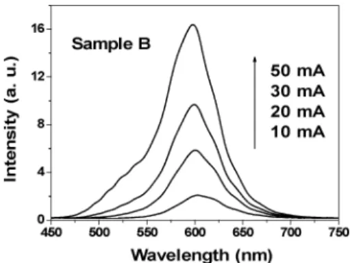
Fig. 3. EL spectra of Sample B (based on the wafer region around one-half radius of the 2-in wafer of the second epitaxy structure) at several injection current levels.
QW has relatively higher indium content. In this situation, spin-odal decomposition may occur to relax the heterostructure strain [11], [12]. Note that the minor peak of Sample C is further red-shifted when compared with that of Sample B. This result is due to the higher indium incorporation at the wafer center under the growth condition of a low wafer rotation speed in our reactor.
Fig. 2 shows the LED output spectra of Sample A at sev-eral injection current levels. The green spectral-peak shifts from 509.8 nm at 10 mA to 504.5 nm at 50 mA. The quite small blue shift (due to the relaxation of the quantum-confined Stark ef-fect [13]) implies that the heterostructure strain is partially re-laxed and spinodal decomposition to form clusters must have occurred. The blue-shift trend in increasing the injection cur-rent is consistent with the observation of PL spectral peak de-pendence on the excitation power. As the excitation power in-creases, the PL spectral peak blue shifts. Fig. 3 shows the LED output spectra of Sample B at several injection current levels. Here, the short-wavelength PL peak is not observed because of the short migration distance of hole [14]. The electrolumines-cence (EL) peak is located around 600 nm without significant blue shift in increasing the injection current. As the injection current increases, a minor EL peak around 525 nm can be seen implying that the indium contents among the five high-indium QWs are nonuniform.
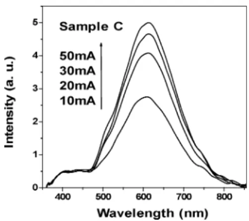
Fig. 4 shows the EL spectra of Sample C at several injec-tion current levels. Here, one can observe even longer wave-length emission, up to 613.1 nm at the peak. The EL spectra in this sample are quite broad. At the injection current of 50 mA,
CHEN et al.: ORANGE–RED LEDs BASED ON A PRESTRAINED InGaN–GaN QW EPITAXY STRUCTURE 2271
Fig. 4. EL spectra of Sample C (based on the wafer region near the center of the 2-in wafer of the second epistructure) at several injection current levels.
Fig. 5. Current versus voltage curves of the three samples.
the full-width at half-maximum of the EL spectrum covers from 532.9 through 691 nm. It is interesting to observe a short-wave-length shoulder extending into the UV range. This result implies that holes can reach the low-indium QW in this device. Fig. 5 shows the comparisons of turn-on voltage and resistance among the three device samples. The current versus voltage curves here show that Samples A and B have the similar turn-on voltages and device resistance values. However, those of Sample C are rela-tively higher. The lager turn-on voltage and device resistance are due to the relatively poorer crystal quality in Sample C.
In summary, we have demonstrated the operations of an or-ange and a red LED, which were fabricated with a prestrained InGaN–GaN QW epitaxy structure. The prestrain condition was created by growing a low-indium QW before the growth of five high-indium QWs. Without the prestrain condition, the five high-indium QW of the same growth condition led to green EL emission. With the prestrained growth, indium incorporation in the QWs grown after the low-indium one became higher and hence orange–red LEDs could be fabricated for elongating the emission wavelength by more than 100 nm. Although we have successfully implemented orange–red LEDs, their crystal
quali-ties need to be improved. Several growth methods, including the migration-enhanced MOCVD [15] and epitaxial over-growth [16], will be used for improving the crystal quality.
REFERENCES
[1] M. Yamada, Y. Narukawa, and T. Mukai, “Phosphor free high-lumi-nous-efficiency white light-emitting diodes composed of InGaN multi-quantum well,” Jpn. J. Appl. Phys., vol. 41, no. 3A, pt. 2, pp. L 246–L 248, Mar. 2002.
[2] D. Xiao, K. W. Kim, S. M. Bedair, and J. M. Zavada, “Design of white light-emitting diodes using InGaN/AlInGaN quantum-well structures,”
Appl. Phys. Lett., vol. 84, pp. 672–674, Feb. 2004.
[3] I. Ozden, E. Makarona, A. V. Nurmikko, T. Takeuchi, and M. Krames, “A dual-wavelength indium gallium nitride quantum well light emit-ting diode,” Appl. Phys. Lett., vol. 79, pp. 2532–2534, Oct. 2001. [4] Y. D. Qi, H. Liang, W. Tang, Z. D. Lu, and K. M. Lau, “Dual
wave-length emission InGaN/GaN multi-quantum well LEDs grown by met-alorganic vapor phase epitaxy,” J. Cryst. Growth, vol. 272/1–4, pp. 333–340, 2004.
[5] J. Ristic, E. Calleja, A. Trampert, S. Fernandez-Garrido, C. Rivera, U. Jahn, and K. H. Ploog, “Columnar AlGaN/GaN nanocavities with AlN/GaN Bragg reflectors grown by molecular beam epitaxy on Si(111),” Phys. Rev. Lett., vol. 94, p. 146102, Apr. 2005.
[6] Y. Sun, Y. H. Cho, H. M. Kim, and T. W. Kang, “High efficiency and brightness of blue light emission from dislocation-free InGaN/GaN quantum well nanorod arrays,” Appl. Phys. Lett., vol. 87, pp. 093115-1–3, Aug. 2005.
[7] A. Kikuchi, M. Kawai, M. Tada, and K. Kishino, “InGaN/GaN mul-tiple quantum disk nanocolumn light-emitting diodes grown on (111) Si substrate,” Jpn. J. Appl. Phys., vol. 43, no. 12A, pp. L1524–L1526, Nov. 2004.
[8] T. Akasaka, H. Gotoh, T. Saito, and T. Makimoto, “High luminescent efficiency of InGaN multiple quantum wells grown on InGaN under-lying layers,” Appl. Phys. Lett., vol. 85, no. 15, pp. 3089–3091, Oct. 2004.
[9] T. Akasaka, H. Gotoh, H. Nakano, and T. Makimoto, “Blue-purplish InGaN quantum wells with shallow depth of exciton localization,”
Appl. Phys. Lett., vol. 86, pp. 191920-1–3, May 2005.
[10] S. M. Ting, J. C. Ramer, D. I. Florescu, V. N. Merai, B. E. Albert, A. Parekh, D. S. Lee, D. Lu, D. V. Christini, L. Liu, and E. A. Armour, “Morphological evolution of InGaN/GaN quantum-well heterostruc-tures grown by metalorganic chemical vapor deposition,” J. Appl.
Phys., vol. 94, pp. 1461–1467, May 2003.
[11] Ho and G. B. Stringfellow, “Solid phase immiscibility in GaInN,”
Appl. Phys. Lett., vol. 69, pp. 2701–2703, Oct. 1996.
[12] Y. S. Lin, K. J. Ma, C. Hsu, Y. Y. Chung, C. W. Liu, S. W. Feng, Y. C. Cheng, M. H. Mao, C. C. Yang, H. W. Chuang, C. T. Kuo, J. S. Tsang, and T. E. Weirich, “Quasiregular quantum-dot-like structure formation with postgrowth thermal annealing of InGaN/GaN quantum wells,” Appl. Phys. Lett., vol. 80, pp. 2571–2573, Apr. 2002. [13] Y. C. Cheng, E. C. Lin, C. M. Wu, C. C. Yang, and J. R. Yang,
“Nanostructures and carrier localization behaviors of green-lumines-cence InGaN/GaN quantum-well structures of various silicon-doping conditions,” Appl. Phys. Lett., vol. 84, pp. 2506–2508, Apr. 2004. [14] K. S. Kim, M. G. Cheong, C. H. Hong, G. M. Yang, K. Y. Lim, E. K.
Suh, and H. J. Lee, “Hole transport in Mg-doped GaN epilayers grown by metalorganic chemical vapor deposition,” Appl. Phys. Lett., vol. 76, pp. 1149–1151, Feb. 2000.
[15] R. S. Qhalid Fareed, R. Jain, R. Gaska, M. S. Shur, J. Wu, W. Walukiewicz, and M. A. Khan, “High quality InN/GaN heterostruc-tures grown by migration enhanced metalorganic chemical vapor deposition,” Appl. Phys. Lett., vol. 84, pp. 1892–1894, Mar. 2004. [16] I. Kidoguchi, A. Ishibashi, G. Sugahara, and Y. Ban, “Air-bridged
lat-eral epitaxial overgrowth of GaN thin films,” Appl. Phys. Lett., vol. 76, pp. 3768–3770, Jun. 2000.