Visible and band edge electroluminescence from indium tin oxide
Õ
SiO
2Õ
Si
metal–oxide–semiconductor structures
Miin-Jang Chen,a)Ching-Fuh Lin,a),b)W. T. Liu, S. T. Chang, and C. W. Liu
Department of Electrical Engineering, National Taiwan University, Taipei, Taiwan, Republic of China 共Received 8 September 2000; accepted for publication 19 October 2000兲
Characteristics of electroluminescence from indium tin oxide (ITO兲/SiO2/Si metal–oxide– semiconductor共MOS兲 structures fabricated on both p-type and n-type Si wafers were investigated. The ITO/SiO2/Si MOS on p-type Si could have both the visible and band edge electroluminescence,
while the ITO/SiO2/Si MOS on n-type Si has only band edge emission. The reason for the
difference is attributed to the impact ionization that only occurs for ITO/SiO2/Si( p) MOS. The
study indicates that the band edge emission and visible luminescence are competing processes. The electroluminescence from ITO/SiO2/Si(n) is also discovered to be less than that from the
Al/SiO2/Si(n). The reason is possibly due to the damage of the oxide bonding and the SiO2/Si
interface during the ITO sputtering. © 2001 American Institute of Physics.
关DOI: 10.1063/1.1331647兴
I. INTRODUCTION
Silicon is the most useful semiconductor material for the integrated-circuit 共IC兲 industry, but its applications in areas of optics and optoelectronics are limited. The main reason is the obstacle of indirect-band-gap characteristics. Thus con-verting silicon to a light-emitting material or causing lumi-nescence on silicon substrates is attractive for research. To overcome the indirect-band-gap obstacle, many efforts were attempted. They include porous-silicon-based devices,1,2 nanocrystalline Si,3,4 Si⫹-implanted SiO2,5 Er-doped Si,6
deposition of polymer on Si substrates,7growth of GaN on Si substrates,8and so on.
The metal–oxide–semiconductor共MOS兲 structures have also been observed to exhibit visible electroluminescence
共EL兲. For example, visible EL has been reported from a
Ag/SiO2/Si structure or similar MOS structures with native
oxide.9,10Because the native oxide usually contains deficient defects and its property strongly relies on the forming environment,11the visible luminescence from MOS with na-tive oxide was explained due to luminescent centers or oxy-gen deficient defects in the native oxide.9,10 On the other hand, visible EL has also been observed from conventional MOS tunneling diodes with the polysilicon gate12as well as from metal–oxide–semiconductor field effect transistor
共MOSFET兲 and p – n junctions fabricated on Si.13,14Impact
ionization was proposed to explain such visible EL.
Recently, we discovered the band edge EL from Al/SiO2/Si MOS structures with the oxide grown by
well-controlled rapid thermal oxidation 共RTO兲.15 Such lumines-cence corresponds well to the band-gap energy and could be explained by the electron–hole recombination.16 In this work, the transparent indium tin oxide 共ITO兲 is used to re-place the Al metal gate15 so that the luminescence can be better investigated. It is discovered that the ITO/SiO2/Si
MOS on p-type Si could have both the visible and band edge EL, while the ITO/SiO2/Si MOS on n-type Si has only the
band edge emission.
II. MEASUREMENTS ON BAND EDGE AND VISIBLE ELECTROLUMINESCENCE
The ITO/SiO2/Si MOS for the investigation has the
ul-trathin gate oxide which allows significant current to tunnel through. The ultrathin gate oxide is grown by the well-controlled RTO. Samples were prepared in two different conditions. Sample A has 3.3 nm gate oxide grown on a p-type wafer at a temperature of 950 °C and a pressure of 500 mbar. Then ITO was immediately deposited by sputter-ing with the sample held at 150 °C. Sample B has 3.1 nm gate oxide grown on a n-type wafer at a temperature of 900 °C and a pressure of 350 mbar, while ITO was immedi-ately deposited by sputtering for the sample held at 100 °C. The p-type Si and n-type Si wafers have a resistivity of 1–5 and 1–10⍀ cm, respectively. At last, Al metals were depos-ited on the back side of the two Si wafers.
Because the basic structure of the ITO/SiO2/Si MOS is
the same as the Al/SiO2/Si MOS, both ITO samples have
their I – V characteristics similar to those of Al/SiO2/Si
MOS, as shown in Fig. 1. Quite fair rectification property was observed. In general, the ITO/SiO2/Si MOS on p-type Si
needs a larger voltage to reach the same forward-bias current than the ITO/SiO2/Si MOS on n-type Si. Because the work function of ITO is close to the Si electron affinity,17 the flatband voltage共absolute value兲 of ITO/SiO2/Si( p) is larger than that of ITO/SiO2/Si(n). This leads to a large applied voltage for the ITO/SiO2/Si( p) MOS tunneling diode during the forward bias.
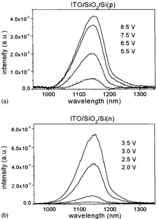
The band edge emission was again observed from the ITO/SiO2/Si MOS on both the p-type and n-type Si. Figures
2共a兲 and 2共b兲 show the spectra of band edge emission for samples A and B, respectively. These spectra were measured using an InGaAs detector placed at the exit of the
monochro-a兲Also with Graduate Institute of Electro-Optical Engineering. b兲Electronic mail: [email protected]
JOURNAL OF APPLIED PHYSICS VOLUME 89, NUMBER 1 1 JANUARY 2001
323
0021-8979/2001/89(1)/323/4/$18.00 © 2001 American Institute of Physics
mator. Because the spectra are the same as those from Al/SiO2/Si MOS, the band edge EL chould be explained by
the electron–hole radiative recombination.16
On the other hand, sample A also has visible EL. In comparison to the band edge EL, the visible EL is very weak and cannot be measured using a Si detector that has similar sensitivity to the InGaAs detector. However, it could be ob-served by the naked eye at the current density as low as 1.4 A/cm2 because it could pass through the transparent ITO. Because the Si detector is unable to detect the visible EL, the visible EL is estimated to be over ten times weaker than the band edge emission. The photomultiplier 共PMT兲 was then used to detect the weak visible EL. Figure 3 shows the
mea-sured visible spectra. The spectral range is limited by the PMT spectral coverage. The peak wavelength of the spectra in Fig. 3 is possibly more than 800 nm. In contrast, no visible spectrum was observed from sample B even when its forward-bias voltage is up to 8 V and the current density is as large as 25 A/cm2.
Figure 4 shows the measured L – I curves for the band edge EL of the two samples. Similar to the band edge EL from Al/SiO2/Si MOS, the slope efficiency increases with
the injection current. Figure 4 also shows that sample B ob-viously has a larger band edge EL efficiency than sample A. The slope efficiency of the EL at the current of 70 mA from samples A and B is about 2⫻10⫺8 and 5⫻10⫺7, respec-tively. The relatively small efficiency of band edge EL and visible EL from sample A should not be a coincidence. The reason could be due to the impact ionization from sample A, as will be explained in the following.
III. DISCUSSION
For the MOS on p-type Si, the major current is contrib-uted from the electrons tunneling from the metal gate to the Si.18Because the ITO/SiO2/Si( p) MOS needs a larger gate
voltage for significant forward-bias current to appear, the ballistic electrons tunneling through the oxide could cause significant impact ionization of the p-type Si.12This creates a large population of holes in the valence band, leading to the
FIG. 1. I – V characteristics of共a兲 ITO/SiO2/Si( p) and共b兲 ITO/SiO2/Si(n). The reversed bias is defined as positive gate voltage for 共a兲 and negative gate voltage for共b兲.
FIG. 2. Band edge electroluminescence spectrum of 共a兲 ITO/SiO2/Si( p) and共b兲 ITO/SiO2/Si(n).
FIG. 3. Visible electroluminescence spectrum of the ITO/SiO2/Si( p).
FIG. 4. L – I curves for共a兲 ITO/SiO2/Si( p) and共b兲 ITO/SiO2/Si(n).
324 J. Appl. Phys., Vol. 89, No. 1, 1 January 2001 Chenet al.
direct recombination of tunneled electrons with those holes. Thus visible EL is emitted. The direct transition of the hot electrons to the valence band reduced the number of elec-trons near the conduction-band minimum, so the band edge EL is reduced. Figure 5 shows the relative intensity of visible EL and band edge EL versus the applied voltage. The shown intensity is normalized to each measured value at 10 V of visible EL and band edge EL, respectively. For the gate volt-age larger than 8.5 V, the visible EL superlinearly increases with the applied voltage because the impact ionization is more significant at a larger voltage. In contrast, the band edge EL only sublinearly increases with the voltage when the applied voltage is large. This study indicates that the band edge EL and visible EL are competing processes for MOS on p-type Si. However, the band edge EL is in general much stronger than the visible EL, so the former process is still preferred in the MOS on p-type Si although it is reduced by the impact ionization under large applied voltages.
For the MOS on n-type Si, the major current is contrib-uted from the electrons tunneling from the Si to the metal gate.18 Therefore the Si semiconductor does not suffer from the impact ionization caused by the ballistic electrons. Al-though there are also some holes tunneling from the metal gate to Si, the amount is relatively small, compared to elec-trons. In addition, the massive holes could hardly cause im-pact ionization on Si.19 Thus the ITO/SiO2/Si(n) MOS
ex-hibits no visible EL even when the bias voltage is up to 8 V. Also, its efficiency of band edge EL is higher because of no competition from the visible EL.
Although the luminescent centers or oxygen deficient defects in the native oxide have been explained as the cause of the visible luminescence from MOS with native oxide,9,10 they are unlikely to be the reason for the visible EL from the ITO/SiO2/Si MOS on p-type Si. Otherwise, the visible EL
should be observed from ITO/SiO2/Si MOS on n-type Si as
well.
IV. EFFICIENCY OF BAND EDGE EMISSION
In the ITO/SiO2/Si MOS, because no light is blocked by
the transparent ITO metal gate, the measurement shown in Fig. 4 seems to be the ultimate light output that can possibly
be generated from such a MOS structure. However, we have observed stronger light output from the Al/SiO2/Si(n) MOS with the RTO grown oxide, the same as the ITO/SiO2/Si(n) MOS. Figure 6 shows the L – I characteristics for the Al/SiO2/Si(n) MOS. The light was measured from a pad of the same circular shape and the same area as the ITO/SiO2/Si(n). Because the Al on the Al/SiO2/Si(n) MOS
almost blocks the entire emitted light, only the scattered power from the periphery of the circular area is detected. However, even though smaller percentages of emitted power were collected from the Al/SiO2/Si(n) MOS, the measured
power is still larger than the ITO/SiO2/Si(n) MOS.
From Fig. 6 the slope efficiency of the EL at a current of 70 mA from the Al/SiO2/Si(n) MOS is about 6.5⫻10⫺7.
The slope efficiency increases with the injection current. At a current of 300 mA, the measured slope efficiency is up to 1.3⫻10⫺6. In the calculation of the efficiency, only the power emitted from the periphery of the circular area was taken into account. If the whole area has the emission, the estimated efficiency of the original EL near the Si/SiO2
in-terface from the Al/SiO2/Si(n) MOS might be more than
10⫺5.
To confirm that the whole circular area of the Al/SiO2/Si
MOS could have the band edge emission, the optical power emitted from the Si side of the Al/SiO2/Si MOS was also
measured. Before the measurement, the Al metal at the Si side was first lapped off and then redeposited, but not di-rectly under the MOS area. Thus the light emitted from the Si side was not blocked by Al metal. It was observed to cover the entire circular area. The measured light power is attenuated by the absorption in the Si wafer, which is about 500 m thick, so it should be less than the original power generated near the Si/SiO2 interface. Even so, the measured
power emitted from the Si side is still about three times larger than that measured from the periphery of the MOS structure on the gate side. The measured spectrum from the Si side is also narrower than that measured from the gate side because the short-wavelength part is more absorbed by the Si wafer, as shown in Fig. 7. In Fig. 7, each spectrum is nor-malized to its own maximum for the comparison of the spec-tral coverage.
FIG. 5. The relative intensity of visible EL and band edge EL vs the applied voltage. The shown intensity is normalized to each measured value at 10 V of visible EL and band edge EL, respectively.
FIG. 6. L – I curve of Al/SiO2/Si(n) MOS.
325
J. Appl. Phys., Vol. 89, No. 1, 1 January 2001 Chenet al.
The reduced light emission from ITO/SiO2/Si(n),
com-pared to the Al/SiO2/Si(n), could be due to the defects in the
oxide or extrinsic surface states.11 The defects are possibly formed by the indium and tin aggregations breaking the ox-ide bonding and damaging the SiO2/Si interface during ITO
sputtering.20,21 The I – V measurements show that the reverse-biased current of ITO/SiO2/Si(n) is almost one order
of magnitude larger than that of Al/SiO2/Si(n), indicating
that damage creates another route for carriers to pass through.
V. CONCLUSION
Both band edge EL and visible EL are observed from ITO/SiO2/Si MOS on p-type Si, while only band edge EL is
observed from ITO/SiO2/Si MOS on n-type Si. The visible
EL is attributed to the impact ionization caused by the bal-listic electrons tunneling from the metal gate to the Si. Also, the impact ionization could reduce the efficiency of the band edge EL. The study indicates that the band edge EL and the visible EL are competing processes. For MOS on n-type Si, negligible impact ionization occurs, so it has no visible EL and the band edge EL is stronger at the same injection cur-rent as compared to MOS on p-type Si. The comparison of ITO/SiO2/Si(n) and Al/SiO2/Si(n) also reveals that the ITO sputtering could possibly damage the oxide bonding and the SiO2/Si interface, leading to the reduced EL efficiency of ITO/SiO2/Si(n).
ACKNOWLEDGEMENT
This work is supported in part by the National Science Council, Taipei, Taiwan, ROC under Contract No. NSC89-2215-E-002-016, No. NSC89-2112-M-002-034, and No. 88-2218-E-002-004.
1L. T. Canham, Appl. Phys. Lett. 57, 1046共1990兲.
2S. Lazarouk, P. Jaguiro, S. Katsouba, G. Masini, S. La Monica, G.
Maiello, and F. Ferrari, Appl. Phys. Lett. 68, 2108共1996兲.
3S. Schuppler, S. L. Friedman, M. A. Marcus, D. L. Adler, Y.-H. Xie, F.
M. Ross, Y. J. Chabal, T. D. Harris, L. E. Brus, W. L. Brown, E. E. Chaban, P. F. Szajowski, S. B. Christman, and P. H. Citrin, Phys. Rev. B
52, 4910共1995兲.
4
D. B. Geohegan, A. A. Puretzky, G. Duscher, and S. J. Pennycook, Appl. Phys. Lett. 73, 438共1998兲.
5L. S. Liao, X.-M. Bao, X.-Q. Zheng, N.-S. Li, and N.-B. Min, Appl. Phys.
Lett. 68, 850共1996兲.
6
M. Matsuoka and S. Tohno, Appl. Phys. Lett. 71, 96共1997兲.
7D. R. Baigent, R. N. Marks, N. C. Greenham, R. H. Friend, S. C. Moratti,
and A. B. Holmes, Appl. Phys. Lett. 65, 2636共1994兲.
8M. Garter, J. Scofield, R. Birkhahn, and A. J. Steckl, Appl. Phys. Lett. 74,
182共1999兲.
9
Y. Q. Wang, T. P. Zhao, J. Liu, and G. G. Qin, Appl. Phys. Lett. 74, 3815
共1999兲.
10J. Yuan and D. Haneman, J. Appl. Phys. 86, 2358共1999兲.
11ULSI Technology, edited by C. Y. Chang and S. M. Sze共McGraw-Hill,
New York, 1996兲.
12R. Versari, A. Pieracci, M. Manfredi, G. Soncini, P. Bellutti, and B. Ricco,
IEEE International Electron Devices Meeting, Paper 31.2, Washington, DC, 1999共unpublished兲.
13Y. Uehara, J. Watanabe, S. Fujikawa, and S. Ushioda, Phys. Rev. B 51,
2229共1995兲.
14A. T. Obeidat, Z. Kalayjian, A. G. Andreou, and J. B. Khurgin, Appl.
Phys. Lett. 70, 470共1997兲.
15C.-F. Lin, C. W. Liu, M.-J. Chen, M. H. Lee, and I. C. Lin, J. Appl. Phys.
87, 8793共2000兲.
16
C. W. Liu, M. H. Lee, M.-J. Chen, I. C. Lin, and C.-F. Lin, Appl. Phys. Lett. 76, 1516共2000兲.
17Y. Park, V. Choong, Y. Gao, B. R. Hsieh, and C. W. Tang, Appl. Phys.
Lett. 68, 2699共1996兲.
18
C. W. Liu, M. H. Lee, C. F. Lin, I. C. Lin, W. T. Liu, and H. H. Lin, 1999 IEEE International Electron Devices Meeting, Paper 31.3, Washington, DC, 1999共unpublished兲.
19C. L. Anderson and C. R. Crowell, Phys. Rev. B 5, 2267共1972兲. 20
Y. Hatanaka, S. Kawai, Y. Suzuki, Y. Asai, and G. Shimaoka, Appl. Surf. Sci. 33Õ34, 792 共1988兲.
21Y. H. Aliyu, D. V. Morgan, and R. W. Bunce, Electron. Lett. 28, 142 共1992兲.
FIG. 7. Band edge electroluminescence spectrum of Al/SiO2/Si(n): 共a兲
measured from the Si-side of the MOS structures;共b兲 measured from the Al gate side under the same bias.
326 J. Appl. Phys., Vol. 89, No. 1, 1 January 2001 Chenet al.