244
Optical Properties of InAs
1–x
N
x
/In
0.53
Ga
0.47
As Single Quantum
Wells Grown by Gas Source Molecular Beam Epitaxy
GUAN-RU CHEN,1HAO-HSIUNG LIN,1,2
JYH-SHYANG WANG,1and DING-KANG SHIH1
1.—Graduate Institute of Electronics Engineering and Department of Electrical Engineering, Na-tional Taiwan University, Taipei, Taiwan 106, Republic of China. 2.—E-mail: [email protected]. edu.tw
Optical properties of InAs1–xNx/In0.53Ga0.47As (hereafter, abbreviated as InAsN/
InGaAs) single quantum wells (SQWs) grown on InP substrates by gas source molecular-beam epitaxy are studied using photoluminescence (PL) measure-ments. By comparing the low-temperature PL spectra of InAs/InGaAs and InAsN/InGaAs SQWs, InAs and InAsN phases are found to coexist in the InAsN layer. Such serious alloy inhomogeneities result in obvious exciton localization by potential irregularities. The blue shift of the PL peak after rapid thermal annealing (RTA) is found to originate mainly from As-N interdiffusion inside the well layer. According to the temperature-dependent PL results, uniformity of the InAsN layer can be effectively improved by RTA, and the exciton local-ization is, thus, relieved. Comparison of luminescence quenching and excitation-power-dependent PL behavior between the QWs with and without nitrogen content suggests that the quality of the QW is degraded by the introduction of nitrogen, and the degradation can only be partially recovered by post-growth RTA.
Key words: InAsN, single quantum well, gas source molecular beam epitaxy
(GSMBE), optical characterization, photoluminescence, inter-diffusion, anneal
INTRODUCTION
Mixed group-V nitride alloys have not drawn much attention until the last few years. With the ad-dition of nitrogen into conventional III-V compound-semiconductor materials, qua or ternary-nitride alloys, such as InGaAsN or GaAsN, are formed, and an obvious bandgap bowing is observed,1–3
which is usually attributed to the much smaller size and large electronegativity of the nitrogen atom. Heterostructures with large conduction-band offsets could be achieved by the use of these materials such that much better temperature characteristics, re-sulting from more efficient carrier confinement, are revealed.1However, for the applications into longer wavelength—for example, mid-infrared—region, there are difficulties in using such materials as GaAsN because quite a large nitrogen content is needed, and many problems on crystal growth burst out. Therefore, more suitable materials should be chosen for such long wavelength applications. The
InAs has a narrow bandgap of 0.36 eV at room tem-perature, and only a little nitrogen incorporation will produce sufficient bandgap bowing to serve the purpose, making InAsN a promising mid-to-far infrared material.4
We had formerly demonstrated a highly strained InAs/InGaAs multiple quantum well (QW) laser on an InP substrate with a 2.2-m lasing wavelength at room temperature.5This kind of QW structure is
promising for applications in the mid-infrared (1.5– 3 m) wavelength range, such as medical care, re-mote sensing, and fluoride-glass fiber used in optical communications. Based on the highly strained InAs/InGaAs QW structure of this device, there are several advantages if we use InAsN to replace InAs as the well-layer material. Because of the bandgap bowing effect, the bandgap energy can be further de-creased to achieve a longer emission wavelength, and the critical thickness of the well layer is in-creased simultaneously, making possible a larger well thickness, which pushes the wavelength longer too. In this article, optical properties of InAsN/In-GaAs-strained single quantum wells (SQWs) grown
on InP substrates are investigated by the photo-luminescence (PL) measurement. The effects of rapid thermal annealing (RTA) will also be discussed and compared with those of the InAs/InGaAs SQW. From the experimental results, InAs and InAsN al-loys are found to coexist in the well layer. The RTA-induced, PL-peak blue shift is attributed not only to the In-Ga interdiffusion between well and barrier but also to the As-N interdiffusion inside the well layer itself. In addition, a comparison of the thermal-quenching behaviors of optimum-condition-annealed InAs/InGaAs and InAsN/InGaAs SQWs shows that a more easily thermally activated, nonradiative-recombination channel is introduced by the incorpo-ration of nitrogen.
EXPERIMENT
The InAs/InGaAs (sample C738) and InAsN/In-GaAs (sample C736) SQWs were grown by a VG (East Grinstead, U.K.) V-80H gas-source molecular-beam epitaxy system.6Active nitrogen species were
pro-vided by an EPI (Woodbury, NY) UNI-bulb, radio-frequency plasma source. A 0.1-m-thick InP buffer layer was grown at first at 450°C, then the growth was interrupted for 8 minutes, followed by the 400°C growth of the InGaAs/InAs(N)/InGaAs SQW struc-ture under a 1-m/h growth rate and an As/In ratio of 2. For the growth of nitrogen-containing QW C736, the radio-frequency plasma power was tuned at 300 W, and the N2flow rate was 1.4 SCCM. The SQWs
are comprised of 100-nm-thick In0.53Ga0.47As barriers
and 30-Å-thick InAs or InAsN well layer. Finally, an InP cap layer with a thickness of 0.1 m was grown on top of the SQW structure. Different post-growth an-nealing conditions ranging from 500–600°C with a duration of 15 min were used. The 514.5-nm line of an argon-ion laser was used in the PL measurement to excite the luminescence. Samples were mounted on the cold finger of a variable-temperature and closed-cycle helium cryostat. The luminescence was col-lected by a CaF2lens and dispersed by a SPEX 500M
monochromator into a liquid-nitrogen-cooled HAMA-MATSU P3357-02 InSb photodiode (with preampli-fier). General lock-in technique was used in our PL measurements. To investigate the optical properties of our as-grown and annealed samples, temperature-de-pendent and excitation-power-detemperature-de-pendent PL mea-surements were carried out. By using temperature-dependent PL measurements, we can observe the PL-peak energy and full-width at half-maximum (FWHM) evolution and the QW thermal-quenching behavior. Excitation-power-dependent PL shows the PL-peak shift and the relation between PL inten-sity and excitation-power deninten-sity. All information obtained will be helpful for us to recognize the luminescence mechanisms inside these QWs.
RESULTS AND DISCUSSION
Owing to a large miscibility gap, III-V-N materials usually have poor alloy uniformity. Sometimes phase separation may even occur. It has been found
by Gas Source Molecular Beam Epitaxy 245
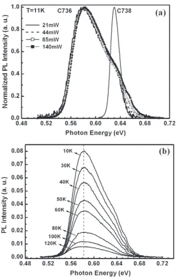
that for InAsN alloys grown by molecular-beam epi-taxy, both the metastable InAsN alloy and the pure InAs could coexist in the film.7,8Figure 1a shows the
11-K PL spectra of a C736 InAsN/InGaAs SQW (as-grown) at different excitation powers along with the PL spectrum of C738 (as-grown). The PL profile of C736 (as-grown) is quite asymmetric, and a shoul-der at about 0.63 eV (position of the C738 PL peak) can be identified, which is believed to be coming from the phase-separated InAs regions in the well layer. The main peak is red shifted by about 50 meV with respect to the C738 PL peak because of the op-tical bowing effect induced by the introduction of nitrogen. Normalized PL spectra at different excita-tion powers show that the relative intensity of the luminescence from the InAsN regions and from the InAs regions almost does not change, indicating similar and uncoupled, excitonic-recombination dy-namics between the two regions. The blue shift of the PL peak with increasing excitation power is due to
Fig. 1. (a) The PL profiles of C736 as-grown InAsN/InGaAs SQW at different excitation-power intensities (21 mW, 44 mW, 85 mW, and 140 mW); all are normalized for convenience of comparison. Also shown is the PL spectrum of C738 as-grown InAs/InGaAs SQW. (b) Temperature-dependent PL spectra (10–120 K) of C736 as-grown InAsN/InGaAs SQW.
band filling to higher energy states in the band tail. The much larger PL FWHM compared with C738 arises mainly from the alloy disorders. From the temperature-dependent PL spectra of C736 (as-grown) in Fig. 1b, we can find that the PL-peak energy remains unchanged up to T ⫽ 80 K. This is a result of exciton localization by potential irregulari-ties, resulting from alloy inhomogeneities. At low tem-peratures, local bandgap minima will act as active re-combination sites as long as the drift times of the photo-generated carriers are smaller than radiative-recombination times. As the temperature increases, more carriers will be able to occupy higher energy states, and the effect of bandgap shrinkage caused by increasing temperature will be compensated.9
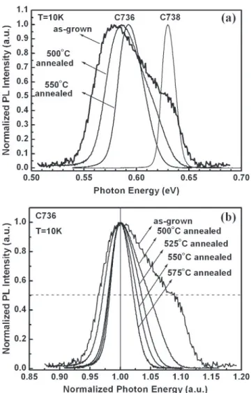
After the discussion of the properties of the as-grown C736 SQW, we now turn to the effects of RTA on this sample. Normalized PL spectra of C736 an-nealed at different temperatures are compared in Fig. 2a. Several characteristics should be noticed here. First, the InAs-related luminescence is
signifi-cantly reduced after annealing, along with a reduced degree of PL-profile asymmetry. Second, the PL FWHM decreases with increasing annealing temper-ature. Third, an obvious blue shift of the PL peak can be observed. If we normalize the photon energy on the x axis with the peak energy set to 1, as shown in Fig. 2b, the differences among these PL spectra will be more clearly identified. The shrinkage of the PL profile at the high-energy side after annealing is much more serious than that at the low-energy side, implying the disappearance of the InAs domain be-cause of As-N interdiffusion. The higher the anneal-ing temperature is, the more symmetric the spec-trum becomes. For samples annealed at T ⬎ 500°C, the low-energy edge is almost fixed, but the high-energy side half width at half maximum continues decreasing.
The 10-K PL-peak energies and FWHMs of differ-ent-temperature-annealed C736 SQWs are shown in Fig. 3. Data of the C738 SQWs are put together for comparison. The PL blue shift of the InAsN/InGaAs SQW after annealing could be attributed to the
In-Fig. 2. (a) The PL profiles of C736 InAsN/InGaAs SQWs after an-nealing at different temperatures. Also shown is the PL spectrum of C738 as-grown InAs/InGaAs SQW. (b) The C736 PL-profile evolu-tion with annealing temperature. Both the PL intensity and the pho-ton energy are normalized for convenience of comparison.
Fig. 3. (a) The C736 10-K PL-peak energies and (b) C736 10-K PL FWHMs at different annealing temperatures. Related data of C738 are also shown for comparison.
by Gas Source Molecular Beam Epitaxy 247
Ga interdiffusion between well and barrier,10,11 the
As-N interdiffusion between well and barrier,12and the As-N interdiffusion inside the well layer itself. The PL blue shift of the C738 SQW unambiguously results from the In-Ga interdiffusion between well and barrier; however, the blue shift of C736 after RTA is obviously larger than that of C738 for an-nealing temperatures below 525°C. According to our previous analyses, this PL shift is dominated by the As-N interdiffusion in the InAsN layer. Such a PL blue shift with increasing annealing temperature, Ta, had also been observed in InGaAsN bulk
mater-ial experimentally.13This kind of diffusion process
may be assisted by defects such that the PL-energy shift gradually decreases at higher annealing tem-peratures because these defects are gradually an-nealed out. Therefore, at higher annealing tempera-tures, the increase of the PL-peak energy follows the trend of C738. Figure 3b shows that the PL FWHM is significantly reduced because of the increased alloy uniformity induced by As-N interdiffusion. It should be noted that the trend of the C736 PL-peak energy increasing and that of the C736 PL FWHM decreasing are the same, again proving that these annealing-temperature-dependent behaviors origi-nate from the same process: the As-N interdiffusion inside the InAsN well layer itself.
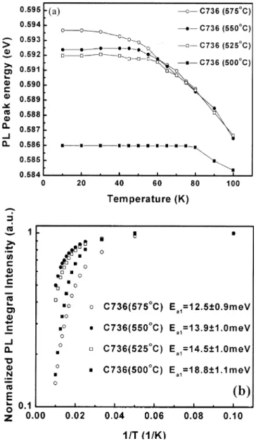
Figure 4a shows the temperature-dependent, PL-peak energies of C736 SQWs annealed at different temperatures. Because the PL process is supposed to be dominated by localized excitons present in po-tential minima induced by alloy disorders, it is not surprising that the PL-peak position does not change much at low temperatures. When the alloy inhomogeneity is reduced with increasing annealing temperature, the temperature dependence of the PL-peak energy starts at lower temperature to fol-low the bandgap red shift. As can be seen, the PL peak stays fixed below T ⫽ 80 K for the 500°C an-nealed sample, but for the sample anan-nealed at 575°C, the PL peak starts to red shift at T ⫽ 40 K. This can be further proved by the thermal-quench-ing behaviors of these samples, as shown in Fig. 4b. Thermal quenching of QW luminescence is usually described by the following equation:14–16
(1)
where IPL is the integrated PL intensity; I0, C1, and
C2are constants; and Ea1and Ea2are activation
ener-gies of nonradiative-recombination channels activated at low and high temperatures, respectively. The term Ea1is proportional to the exciton-localization energy.14
When the temperature increases, excitons are ther-mally excited out of local potential minima and the probability of nonradiative recombination is increased, resulting in the quenching of luminescence intensity. Further increase of temperature will activate the sec-ond (Ea2-related) nonradiative-recombination process,
IPL⫽
I0
1⫹ C1 exp (⫺Ea1/kT)⫹ C2 exp (⫺Ea2/kT)
which seriously quenches the luminescence. In Fig. 4b, the investigated temperature range is from 10 K to 100 K, and the second nonradiative-recombination channel is not activated yet. Therefore, C2 is set to
zero, and the obtained activation energy Ea1is related
to the exciton-localization energy induced by poten-tial irregularities. The term I0is set to 1 because the
integrated intensities are normalized. From the fit-ting results summarized in Fig. 4b, the value of Ea1
decreases with increasing Ta, implying an
elimina-tion of some band-tail states by RTA because of the improved material uniformity. This is consistent with the previous argument that exciton localization origi-nates from alloy disorders.
Finally, to evaluate the quality of the InAsN/In-GaAs SQW, we compare the PL-measurement results Fig. 4. (a) The temperature dependence of PL-peak energies of C736 SQWs annealed at different temperatures and (b) thermal quenching of C736 SQWs annealed at different temperatures. Acti-vation energy Ea1is obtained by using the equation IPL⫽1/(1 ⫹C1
of the SQWs annealed under optimum conditions: C738 (600°C) and C736 (550°C). The Ea2values
ob-tained from the analysis of their thermal-quenching behaviors using Eq. 1 are about 103 meV and 85 meV for C738 (600°C) and C736 (550°C), respectively. The nonradiative-recombination process described by Ea2
might be phonon emission by electrons excited to high-energy states or exciton trapping at interfacial defects.17The term Ea2of C738 (600°C) is close to the
fitting result of InAs/InGaAs SQW obtained by Tournié et al.,18whose value is 110 meV. The much smaller Ea2 value of C736 (550°C) compared with
C738 (600°C) means that the incorporation of nitro-gen into the well layer produces a more easily acti-vated, nonradiative-recombination channel. Excita-tion-power-dependent PL was measured for both the samples, and the results are compared in Fig. 5. The obtained ␣ values in the relation IPL⬀ Iex␣, where IPL
is the integrated PL intensity, and Iexis the
excita-tion intensity, are shown in the figure. According to Fouquet and Siegman,19␣ ⫽ 1 if the radiative-recom-bination process is excitonic, and ␣ ⫽ 2 represents a bimolecular, free-carrier recombination process; meanwhile, nonradiative recombination dominates. The ␣ values of C738 (600°C) remain around ␣ ⫽ 1 until room temperature, indicating that the recombi-nation in this sample is excitonic even at high tem-peratures. However, the ␣ values of C736 (550°C) have a rising trend, meaning that the recombination is gradually dominated by free carriers when the nonradiative recombination is activated. According to the preceding discussions, the quality of InAsN/ InGaAs SQW is still worse than InAs/InGaAs SQW even after RTA treatment. Defects acting as non-radiative-recombination centers are introduced by the introduction of nitrogen and difficult to be fully removed by thermal annealing.
CONCLUSIONS
Optical properties of InAsN/InGaAs SQWs have been studied using PL measurements. Phase sepa-ration into InAs and InAsN regions inside the well layer is observed such that the exciton localization inside the InAsN well is mostly due to serious alloy nonuniformity. By careful inspection of the PL profiles at different annealing temperatures, the PL-peak shift and FWHM reduction after annealing are obvi-ously influenced by the N-As interdiffusion process in the well layer. According to the temperature-dependent PL-measurement results, the exciton-localization effect induced by alloy disorders can be lessened by RTA. A comparison of an optimum-condition-annealed C738 InAs/InGaAs SQW and a C736 InAsN/InGaAs SQW shows that the introduc-tion of nitrogen into the InAs well layer will degrade the optical quality of the QW structure, and the degradation is difficult to be completely recovered by post-growth RTA treatments.
ACKNOWLEDGEMENTS
This work was supported by the National Science Council, Republic of China, under Contract No. NSC 90-2215-E-002-030.
REFERENCES
1. M. Kondow, T. Kitani, S. Nakatsuka, M.C. Larson, K. Nakahara, Y. Yazawa, M. Okai, and K. Uomi, IEEE J. Sel.
Top. Quantum Electron. 3, 719 (1997).
2. S.H. Wei and A. Zunger, Phys. Rev. Lett. 76, 664 (1996). 3. M. Weyers, M. Sato, and H. Ando, Jpn. J. Appl. Phys. 31,
L853 (1992).
4. H. Naoi, Y. Naoi, and S. Sakai, Solid-State Electron. 41, 319 (1997).
5. J.S. Wang, H.H. Lin, and L.W. Sung, IEEE J. Quantum
Electron. 34, 1959 (1998).
6. J.S. Wang and H.H. Lin, J. Vac. Sci. Technol. B 17, 1997 (1999).
7. R. Beresford, K.S. Stevens, and A.F. Schwartzman, J. Vac.
Sci. Technol. B 16, 1293 (1998).
8. M. Hao, S. Sakai, T. Sugahara, T.S. Cheng, and C.T. Foxon,
J. Cryst. Growth 189/190, 481 (1998).
9. H.I. Jeon, M.S. Jeong, H.W. Shim, Y.G. Shin, K.Y. Lim, E.-K. Suh, and H.J. Lee J. Cryst. Growth 171, 349 (1997). 10. H.P. Xin, K.L. Kavanagh, Z.Q. Zhu, and C.W. Tu, Appl.
Phys. Lett. 74, 2337 (1999).
11. H.P. Xin, K.L. Kavanagh, Z.Q. Zhu, and C.W. Tu, J. Vac.
Sci. Technol. B 17, 1649 (1999).
12. L.H. Li, Z. Pan, W. Zhang, Y.W. Lin, Z.Q. Zhou, and R.H. Wu, J. Appl. Phys. 87, 245 (2000).
13. T. Kitatani, K. Nakahara, M. Kondow, K. Uomi, and T. Tanaka, J. Cryst. Growth 209, 345 (2000).
14. J.D. Lambkin, L. Considine, S. Walsh, G.M. O’Connor, C.J. McDonagh, and T.J. Glynn, Appl. Phys. Lett. 65, 73 (1994). 15. E.M. Daly, T.J. Glynn, J.D. Lambkin, L. Considine, and S.
Walsh, Phys. Rev. B 52, 4696 (1995).
16. W.Z. Shen, S.C. Shen, W.G. Tang, Y. Zhao, and A.Z. Li,
J. Appl. Phys. 78, 5696 (1995).
17. D.R. Storch, R.P. Schneider, and B.W. Wessels, J. Appl.
Phys. 72, 3041 (1992).
18. E. Tournié, K.H. Ploog, and C. Alibert, Appl. Phys. Lett. 61, 2808 (1992).
19. J.E. Fouquet and A.E. Siegman, Appl. Phys. Lett. 46, 280 (1985).
Fig. 5. The ␣’s obtained from IPL⬀Iex␣at different temperatures. The