Carrier lifetime measurement on electroluminescent metal–oxide–silicon
tunneling diodes
Miin-Jang Chen,a)Ching-Fuh Lin,a),b)M. H. Lee, S. T. Chang, and C. W. Liu Department of Electrical Engineering, National Taiwan University, Taipei 106, Taiwan 共Received 13 February 2001; accepted for publication 20 July 2001兲
The temporal response of the electroluminescence at the Si band gap energy from a metal–oxide– silicon共MOS兲 tunneling diode is used to characterize the minority carrier lifetime near the Si/SiO2
interface. The temporal responses reveal that the Shockley–Read–Hall 共SRH兲 recombination lifetimes are 18 and 25.8s for the rising and falling edges, respectively, and that the ratio for SRH, radiative, and Auger recombinations is 1:0.196:0.096 at injection current density of 39 A/cm2. The investigation shows that the electroluminescence of the MOS tunneling diode can be significantly increased by reducing the number of the nonradiative recombination centers. © 2001 American
Institute of Physics. 关DOI: 10.1063/1.1405429兴
When the dimensions of metal–oxide–semiconductor field-effect transistors 共MOSFETs兲 are scaled down to the deep submicrometer level in state-of-the-art ultralarge-scale integration共ULSI兲 circuits, the thickness of the gate oxide is in the range of 15–30 Å.1Characterization of MOS devices with such thin gate oxides requires accurate determination of material parameters like the minority carrier lifetime near the Si/SiO2interface to give the information about the low defect
densities present in the ULSI circuits. Conventional methods including high-low frequency capacitance–voltage analysis, the conductance method, the charge pumping method, and transient capacitance–time Zerbst analysis, etc. have been used to measure the minority carrier lifetime and the density of the interface states of MOS devices with relatively thick gate oxides.2– 4However, as the thickness of the gate oxide shrinks, the leakage current tunneling through the ultrathin gate oxide increases. Therefore, the ultrathin oxide compli-cates the analysis and causes modeling based on the above measurement technologies to be difficult.5–7 As a result, a new and simple method needs to be developed to character-ize MOS devices with significant tunneling current. Optical methods, such as photoconductance and photoluminescence decay,4,8,9 have been used to measure the minority carrier lifetime in Si. But the optical method is not suitable for the MOS structure because of the difficulty of optical pumping through the metal gate. In this letter, we report that the elec-troluminescence 共EL兲 at the Si band gap energy10–14 from silicon MOS tunneling diodes provides an easy way by which to probe the minority carrier lifetime and to provide related information about carrier recombination processes near the Si/SiO2 interface.
Rapid thermal oxidation was used to grow ultrathin ox-ide on an n-type wafer with resistivity of 1–10 ⍀ cm. The fabrication process is similar to previously reported ones.10–14The peak emission energy of the EL is around 1.08 eV.10–14The temporal response of the EL under injection of a square current pulse was measured using a scanning-gate in-tegrator and a boxcar averaging system.15 The experimental
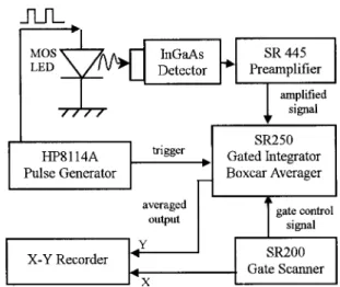
setup is schematically shown in Fig. 1. A MOS light-emitting diode was driven by a square pulse current generated from an HP8114A. An InGaAs detector with a diameter of 5 mm was placed close to the MOS light-emitting diode to collect the luminescence. A preamplifier 共model SR445, Stanford Re-search Systems兲 with 300 MHz bandwidth was used to am-plify the signal. The amplified signal was sent to a SR250 gated integrator and the boxcar averager. The gated integra-tor integrates and normalizes the signal during the gated pe-riod. The boxcar averages the output over many shots of injection current. The gate delay was scanned by applying a control voltage from a SR200 gate scanner to allow retrieval of the entire EL wave form. The bandwidth of the overall measurement system was tested by a commercial light-emitting diode, which typically has modulation bandwidth far above several MHz. The response time of the overall measurement system was found to be much faster than the temporal response of the MOS light-emitting diodes. This ensures the feasibility of wave form retrieval of the EL signal using the scanning gate integrator and boxcar averager.
The temporal response of the EL under injection of a square current pulse of 150 s duration is shown in Fig. 2. Figure 2共a兲 shows the typical wave form of the injection
a兲Also at the Graduate Institute of Electro-Optical Engineering.
b兲Electronic mail: [email protected] FIG. 1. Schematic of the experimental setup for the measurement of tem-poral response.
APPLIED PHYSICS LETTERS VOLUME 79, NUMBER 14 1 OCTOBER 2001
2264
current. Figure 2共b兲 shows the measured temporal wave forms of the EL from the MOS tunneling diode at various injection currents. The measured temporal EL signals track the variation of the excess minority carrier density over time.4 Because of the RC time constant of the MOS struc-ture, the injection current pulse rises and falls in a sluggish manner rather than in the very fast response time共⬃10 ns兲 of the HP8114A. However, a comparison of Figs. 2共a兲 and 2共b兲 shows that the temporal response of the injection current pulse is still much faster than the response of the EL signal. Therefore, the minority carrier lifetime at the Si/SiO2
inter-face can be determined by either the rising edge or the falling edge of the EL response curve.
The theoretical fitting curves in Fig. 2共b兲, indicated by the thick dashed lines, are obtained by solving the following equation:4
d P
dt ⫽G⫺共AP⫹BNP⫹CN
2P兲, 共1兲
where P is the excess minority carrier density, N is the ma-jority carrier density, and G is the generation rate of the excess minority carrier density due to the injection current. A is the coefficient of the Shockley–Read–Hall共SRH兲 recom-bination through the states near the Si/SiO2 interface. B and
C are band-to-band radiative recombination and Auger
re-combination coefficients, respectively. The rising and falling edges of the temporal EL wave forms were fitted using the exponential function with the time constant related to co-efficients A, B, and C:
1
⫽A⫹BN⫹CN2. 共2兲
Figure 2共b兲 shows a good match between the experimen-tal data and the fitting curves. The toexperimen-tal carrier recombination rates 1/ extracted from the curve fitting in Fig. 2共b兲 are shown in Fig. 3. The values of deduced are in agreement with the minority carrier lifetime of 1–100 s for state-of-the-art ULSI technology.3At the rising edge of the EL, the recombination rate is independent of the injection current level. This can be attributed to the dominant process of SRH recombination according to Eq. 共2兲. On the other hand, the recombination rate slightly increases with the injection cur-rent at the falling edges of the EL signal. Since the majority carrier density at the accumulation layer increases with ap-plied voltage, this indicates that the effect of radiative and Auger recombination cannot be neglected at the EL falling edge.
It is known that Si/SiO2 interface states with energies
near the Fermi level are the most active SRH recombination centers2– 4and that the SRH recombination rate approaches a maximum when the recombination centers are near the mid-gap region.16 Just as the current is turned on 共rising edge兲, the MOS diode is still near the flat-band condition and the position of the Fermi level is close to midgap. Thus the SRH recombination rate is large and depends less on the carrier density N because there is no large accumulation of carriers near the Si/SiO2 interface. At the falling edge, the MOS is
already at the accumulation region. Then the Fermi level in
n-type Si is located near the conduction band edge, leading
to the reduced SRH recombination rate, compared to that the rising edge. Also, the Fermi level has negligible variation with the injection current, so the SRH recombination is con-stant in the case of the accumulation region. In addition, the near-conduction-band Fermi level results in a very large ac-cumulated majority carrier density. This causes the relatively strong influence of carriers on the recombination rate.
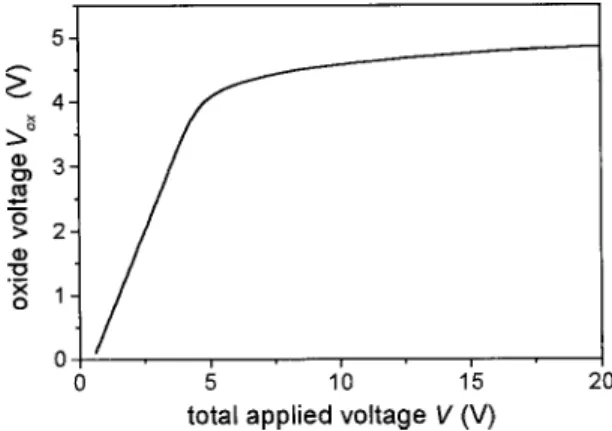
As shown in Fig. 3, the recombination rate at the EL falling edge superlinearly increases with the injection cur-rent. Using the least squared method, a parabolic curve can fit these data points well. The relation between current den-sity J and carrier denden-sity N is usually given by J⫽TqNv,17 where T is the tunneling probability across the oxide. Its value depends on the oxide voltage Vox.4,17 Figure 4 shows
the calculated Vox vs V共the total applied voltage across the
MOS tunneling diode兲 using the equations of tunneling cur-rent in Ref. 4. The thickness of the gate oxide is 30 Å, the gate area is 0.0154 cm2, and the resistance of the Si substrate
FIG. 2.共a兲 Typical wave form of the injection current with a duration of 150
s and共b兲 temporal EL wave form from the MOS tunneling diode at various injection currents.
FIG. 3. Total carrier recombination rates 1/vs the injected current level at the EL rising and falling edges. The dashed lines are the theoretical fitting.
2265 Appl. Phys. Lett., Vol. 79, No. 14, 1 October 2001 Chenet al.
is ⬃15 ⍀, respectively. When V is greater than 5 V, the major voltage drop is on the Si substrate due to the high injection current, so the increase of the oxide voltage Vox is
small. Hence, at large applied voltages, the tunneling prob-ability T approaches a constant4 to give an approximately linear relation between the current density J and the carrier density N, N⫽kJ. Thus Eq. 共2兲 gives the parabolic relation between the recombination rate 1/and current density J:
1
⫽A⫹BkJ⫹Ck2J2. 共3兲
Therefore, the measurements shown in Fig. 3 reveal the rela-tive roles of SRH recombination, radiarela-tive recombination, and Auger recombination.
From the intercept of the fitting curves in Fig. 3 and from Eq. 共3兲, the SRH recombination lifetimes SRH (SRH
⫽1/A) are 18 and 25.8 s for the rising and falling edges, respectively. The parabolic curve in the falling edge also gives the values of Bk and Ck2, which are 194.6 cm2/A s and 2.4 cm4/A2s, respectively. The ratio for SRH, radiative, and Auger recombinations is 1:0.196:0.096 at injection current density of 39 A/cm2. In the falling edge, the SRH recombi-nation is still the most important process, but the contribu-tions from radiative and Auger recombination cannot be ig-nored. Our study reveals that reducing the number of SRH recombination centers should improve the EL efficiency of the MOS tunneling diode.
If the Auger recombination coefficient C⫽10⫺31cm6/s for holes in bulk Si is used,4the value of coefficient B can be determined to be 4⫻10⫺14cm3/s. It is about 10 times larger
than that reported for bulk silicon.4The increased radiative recombination could be due also to the assistance of interface roughness and localized carriers for MOS tunneling diodes.10–13
In conclusion, the temporal response of a light-emitting MOS silicon tunneling diode was measured. The minority carrier lifetimes were deduced from the temporal EL wave forms. At the rising edge of the EL, SRH recombination is the only significant process, while at the falling edge radia-tive and Auger recombination show importance. The study indicates that reducing the number of nonradiative recombi-nation centers should increase the electroluminescence of a MOS tunneling diode.
This work was supported in part by the National Science Council, Taipei, Taiwan, Republic of China, under Contract Nos. NSC89-2215-E-002-016, NSC89-2112-M-002-034, and 88-2218-E-002-004.
1E. J. Lerner, IBM J. Res. Dev., 6共1999兲.
2E. H. Nicollian and J. R. Brews, MOS Physics and Technology共Wiley,
New York, 1982兲.
3T. Hori, Gate dielectrics and MOS ULSIs: Principles, Technologies, and Applications共Springer, Berlin, 1997兲.
4D. K. Schroder, Semiconductor Material and Device Characterization,
2nd ed.共Wiley, New York, 1998兲.
5K. J. Yang and C. Hu, IEEE Trans. Electron Devices 46, 1500共1999兲. 6
K. Ahmed, E. Ibok, G. C.-F. Yeap, Q. Xiang, B. Qgle, J. J. Wortman, and J. R. Hauser, IEEE Trans. Electron Devices 46, 1650共1999兲.
7W. K. Henson, K. Z. Ahmed, E. M. Vogel, J. R. Hauser, J. J. Wortman,
R. D. Venables, M. Xu, and D. Venables, IEEE Electron Device Lett. 20,
179共1999兲.
8
ASTM Standard F28-91, 1996 Annual Book of ASTM Standards
共American Society for Testing Materials, West Conshohocken, PA, 1996兲. 9G. Bohnert, R. Hacker, and A. Hangleiter, J. Phys.共Paris兲, Colloq. 4, 617
共1988兲. 10
C.-F. Lin, C. W. Liu, M.-J. Chen, M. H. Lee, and I. C. Lin, J. Appl. Phys. 97, 8793共2000兲.
11C. W. Liu, M. H. Lee, M.-J. Chen, I. C. Lin, and C.-F. Lin, Appl. Phys.
Lett. 76, 1516共2000兲.
12C. W. Liu, M.-J. Chen, I. C. Lin, M. H. Lee, and C.-F. Lin, Appl. Phys.
Lett. 77, 1111共2000兲.
13C. W. Liu, M. H. Lee, M.-J. Chen, C.-F. Lin, and M. Y. Chern, IEEE
Electron Device Lett. 21, 601共2000兲.
14M.-J. Chen, C.-F. Lin, W. T. Liu, S. T. Chang, and C. W. Liu, J. Appl.
Phys. 89, 323共2000兲.
15
Stanford Research Systems, Inc., Operating Manual of Fast Gated Integrators and Boxcar Averagers, Ver. 2.1.
16S. M. Sze, Physics of Semiconductor Devices, 2nd ed.共Wiley, New York,
1981兲.
17
J. G. Simmons, J. Appl. Phys. 34, 1793共1963兲.
FIG. 4. Calculated oxide voltage vs total applied voltage.