The effect of oxygen-to-argon ratio on the electrical and
reliability characteristics of sputtered Sr Bi Ta Nb O
0.8 2.5 1.2 0.9 9qxthin films
M.S. Tsai, T.Y. Tseng
UDepartment of Electronics Engineering and Institute of Electronics, National Chiao Tung Uni¨ersity, Hsinchu 30050, Taiwan Received 11 December 1999; received in revised form 7 June 2000; accepted 7 June 2000
Abstract
This work investigated how the annealing process affects the ferroelectric properties of thin films of Sr0.8Bi Ta2.5 1.2Nb O0.9 9qx
ŽSBTN on IrrSiO rSi substrates prepared by two-target off-axis rf magnetron sputtering at various O r ArqO mixing ratios. 2 2 Ž 2.
ŽOMR with a substrate temperature of 570. ⬚C. Experimental results indicated that the annealing could effectively result in a
large remanent polarization. The remanent polarization, dielectric constant and leakage current of 598⬚C post-annealing SBTN thin films increased with an increase in the OMR and reached a maximum value at 40% OMR. In addition, the results obtained from the dielectric constant and the leakage current were interpreted in terms of polarization effect and loss theory. The 400-nm
thick 40% OMR SBTN films with 598⬚C post-annealing exhibited good surface morphology and had a dielectric constant of 752, a
loss tangent of 0.035 at 100 kHz, a leakage current density of 6=10y6Arcm2at an electric field of 50 kVrcm with a delay time
Ž . 2 Ž .
of 30 s, a remanent polarization 2 Pr of 40 Crcm , a coercive field 2 E of 77 kVrcm at an applied voltage of 3 V, and ac
measured value of Qsw of 20 Crcm2. According to studies on the 10-year lifetime of time-dependent dielectric breakdown
ŽTDDB , high OMR samples have a longer lifetime than the other lower OMR samples. The SBTN films demonstrated fatigue.
free characteristics up to 1011switching cycles under a 3-V bipolar 1 MHz square wave. Moreover, the polarization of the films
Ž .
decreases slightly less 0.5% per decade with retention time up to 240 min.䊚 2000 Elsevier Science S.A. All rights reserved.
Keywords: Sputtering; SBT; Reliability; Ferroelectric properties
1. Introduction
Ferroelectric materials have remanent polarization with two distinct states which an applied electric field can reverse. These materials have the potential for non-volatile random access memory applications ŽNVRAM. w1᎐4 . Ferroelectric memories offer severalx advantages over silicon-based memories, such as faster write speeds and lower operating voltages. As is in-creasingly being recognized, ferroelectric thin films,
Ž .
such as lead zirconate titanate PZT , are highly promising for non-volatile memory applications, e.g.
U
Corresponding author. Tel.:q886-572-1879; fax: q886-573-4361.
Ž .
E-mail address: [email protected] T.Y. Tseng .
Ž . w x
ferroelectric RAM devices FRAM 5,6 . These ferro-electric films exhibit properties capable of satisfying the basic materials requirement for low power memory applications; these properties have a high remanent polarization, low coercive fields, and high resistance. However, PZT materials for FRAM device applications and fabrications still have several problems, such as fatigue, aging, retention, and imprint. Among them, fatigue, i.e. a decrease in switchable polarization with an increasing number of polarization reversals, is a pertinent reliability issue for FRAM devices using a
Ž
destructive readout operation switching of polarization .
at each readrwrite operation . Applying oxide elec-trodes is an effective means of improving the fatigue
w x
characteristics of PZT-based capacitors 7 . Although
0040-6090r00r$ - see front matter 䊚 2000 Elsevier Science S.A. All rights reserved. Ž .
the above techniques have improved the fatigue rate of PZT-based thin films, the electrical conductivity of oxide electrodes is not as high as those of the metal electrodes normally used, such as Pt. Lower conductiv-ity of the oxide electrodes can induce undesirable char-acteristics of ferroelectric NVRAM, such as a higher RC time constant of the capacitor. In addition, oxide electrodes may lead to the formation of secondary non-ferroelectric phases during film growth if
process-w x ing conditions are not carefully controlled 8 .
Recent investigations have examined the feasibility of alternative materials, such as bismuth-layered oxides having a perovskite-like layer-type structure, for FRAM
w x
applications 9᎐13 . These investigations have identified thin films of bismuth-layered oxides, e.g. SrBi Ta O2 2 9 ŽSBT as fatigue-free materials displaying nearly no.
Ž .
change less than 5% in remanent polarization up to 1012 switching cycles with Pt electrodes. Owing to the characteristics of resistance to fatigue, these layered bismuth oxides are considered to be the optimum material for NVRAM applications. Although con-sidered highly promising for NVRAM applications, SBT thin films have not been completely characterized.
Commercialization of non-volatile FRAM tech-nology based on SBT has been hampered by problems
Ž .
related to a high processing temperature )750⬚C ,
Ž .
low remanent polarization 2 P , and low Curie tem-r Ž .
perature T , thereby making direct integration intoc w x high density CMOS devices extremely difficult 14 . In general, the difficulty in reducing the post-deposition annealing temperature of SBT thin films was largely attributed to poor ferroelectric properties at an anneal-ing temperature lower than 700⬚C. Recent
investiga-Ž .
tions indicated that Sr Bi Ta0.8 2.5 1.2Nb O0.9 9qx SBTN can
Ž .
reduce the processing temperature ;600⬚C and im-prove the ferroelectric properties, as well as achieve a
w x
higher P and higher T than SBT 7,14r c ᎐17 . Therefore,
SBTN is a highly promising material for memory appli-cations. Moreover, related investigations have con-firmed the important role which oxygen vacancies play in the fatigue and reliability properties of ferroelectric
w x
films 6,7 . However, a systematic study of the effect of
Ž . Ž .
O2r ArqO mixing ratio OMR during rf sputtering2 on the dielectric and electrical properties of SBTN thin films is generally lacking. In this work, we investigated the structural, electrical and dielectric properties of SBTN films on IrrSiO rSi substrates at a low tempera-2 ture of 570⬚C prepared by two-target off-axis rf sputter-ing at various OMR.
2. Experimental
SBTN thin films were deposited on an Irr
Ž .
SiO2r 100 Si bottom storage node electrode by
two-target off-axis rf magnetron sputtering. The starting p-type silicon wafer was cleaned by the standard RCA
cleaning process and then chemically etched in a dilute HF solution. The 100-nm thick SiO layer was ther-2 mally grown at 1050⬚C in a dry oxidation furnace. The 100-nm thick Ir bottom electrode on the SiO2rSi subs-trate was deposited using a separate sputtering system. Next, the Ir film was prepared at a fixed power of 50 W Žthe power density was 2.55 Wrcm , a constant pres-2. sure of 5 mtorr and substrate temperature of 350⬚C. The measured resistivity of Ir was approximately 27 ⍀rcm at room temperature.
The SBTN films were deposited on Ir by simultane-ous magnetron sputtering from two different sintered targets of Sr Bi Ta0.8 2.2 1.2Nb O and Bi O with a di-0.8 9 2 3
ameter of 2 inches and a thickness of 1r8 inch, synthe-sized using the standard solid-state reaction process. The Bi O target was used to compensate for Bi atoms2 3 in the deposited film because the Bi content in the film generally deviates strikingly from that of the target at a high substrate temperature. The sputtering chamber was then evacuated to a base pressure of 10 mtorr. All films were prepared at a fixed power of 100 W for the
Ž
Sr Bi Ta0.8 2.2 1.2Nb O target the power density was 5.100.8 9 2
. Ž
Wrcm and 20 W for Bi O target power density is2 3 2
.
1.01 Wrcm . A constant chamber pressure of 20 mtorr was maintained by a mixture of argon and oxygen at various mixing ratios ranging from 1:1 to 1:0 with a total flow of 2 sccm. The target-to-substrate separation was approximately 5 cm. All of the SBTN films de-posited at 570⬚C had the same thickness of approxi-mately 400 nm. The deposition rate was approxiapproxi-mately
˚
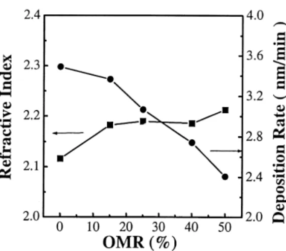
24᎐35 Armin at 570⬚C, as depicted in Fig. 1. According to this figure, the deposition rate decreased with in-creasing OMR, which was attributed to a decrease of the Ar flow. The 50-nm thick Pt top electrodes with diameters of 165, 255 and 350 m, respectively, were then formed by dual E-Gun deposition and patterned by the shadow mask process. Finally, to understand the effect of post-annealing, part of the SBTN thin films
Ž .
after deposition with Pt top electrode were annealed at temperatures ranging from 598 to 673⬚C in a vacuum with pressure of 10 mtorr for 30 min.
The film thickness was determined from ellipsome-try. The thickness measurement was further verified by examining the cross section of the film via scanning electron microscopy. The structure was characterized
Ž .
by X-ray diffraction XRD; Siemens D5000 . Based on XRD data, the average grain size could be determined
w x
by Scherrer’s formula 18 . The chemical composition was estimated by inductively coupled plasma atomic
Ž
emission spectrometry ICP-AES; Perkin-Elmer SCIEX .
ELAN 5000, USA . The surface roughness and mor-phology were examined by atomic force microscopy ŽAFM; Digital Instruments Nano-Scope III . Next, the. depth profiles of oxygen near the interface of SBTNrbottom electrodes were analyzed by secondary
Ž
Fig. 1. The change in refractive index and deposition rate of SBTN thin films with various OMR.
. Ž .
France . The capacitance᎐voltage C᎐V characteris-tics were measured on the metal᎐insulator᎐metal ŽMIM structure by measuring the capacitance at 100. kHz as a function of a swept positive-to-negative volt-age bias. The dielectric constants of the films were then calculated from the capacitance measured at 100 kHz without bias voltage. The dielectric properties were measured as a function of frequency with a
Ž .
Hewlett᎐Packard HP 4194A impedance-gain phase
Ž .
analyzer. The current᎐voltage I᎐V was measured by measuring the current through the sample using HP4145B. A Pt top electrode of the SBTN capacitor was connected to the voltage source and the bottom electrode was grounded. Notably, the polarity was posi-tive when a posiposi-tive voltage was applied to the top
Ž
electrode. The ferroelectric properties fatigue, reten-.
tion and polarization-electric field of the films were measured using RT66A ferroelectric tester from Radi-ant Technologies. All data reported herein are the average values of ten specimens.
3. Results and discussion
Fig. 1 depicts the change in refractive index of SBTN thin films deposited at 570⬚C at various OMR. Accord-ing to this figure, the refractive index of SBTN thin films increases with increasing OMR. Fig. 2a displays the XRD patterns of 400-nm thick SBTN thin films deposited at 570⬚C at 0, 25, 40 and 50% OMR. The film deposited at 0% OMR revealed that diffraction
Ž . Ž .
peaks appeared only from the Ir film and 008 , 115 , Ž028 and 220 peaks of perovskite SBTN structure,. Ž .
Ž . Ž .
implying the absence of 200 and 0010 peaks. Al-though films deposited at 25 and 40% OMR contained
Ž .
the 200 peak of the perovskite SBTN structure, this
Ž .
peak had a low intensity. In addition, the 200 and Ž0010 peak intensities of the SBTN films increased. with an increase in OMR. Comparing stronger and
Ž . Ž .
sharper perovskite peaks of 200 and 0010 from the
50% OMR films with those from the films deposited at a lower OMR revealed an improved crystallinity at high OMR films. This increased crystallinity may have con-tributed to the enhancement in the index of refraction with increasing OMR, as illustrated in Fig. 1. Fig. 2b displays the XRD patterns of 40% OMR films at 598⬚C and 673⬚C post-annealing. According to this figure, the Ž200 and 115 peaks of the 598. Ž . ⬚C post-annealing film were stronger and sharper than those of the 673⬚C post-annealing and as-deposited films. Hence, 598⬚C post-annealing can enhance the grain growth of the SBTN thin films in the a-axis and c-axis directions, and improve the crystallinity of the film. The variation of
Ž . Ž .
reflections from the 008 and 0010 planes present in
Ž .
the XRD pattern of SBTN Fig. 2b could be attributed
Ž .
to the change of the 111 texture in the underlying Ir bottom electrode during annealing. On the basis of the
Ž .
results shown in Fig. 2, the peaks from 00 l planes were small. It is known that SBT thin films exhibit a large polarization along the a- or b-axis; therefore, the orientation indicated in Fig. 2 was preferable to obtain large polarization.
Fig. 3 illustrates the atomic composition of various OMR SBTN thin films with 598⬚C, 640⬚C, and 673⬚C post-annealing. This composition, determined from
Ž .
Fig. 2. XRD patterns of SBTN thin films with: a various OMR Ž .
ICP-AES, was represented by the atomic ratios of Bi,
Ž .
Sr, and Nb to Ta s1.2 . An average atomic ratio of SrrNbrTa was approximately 0.8:0.9:1.2, and almost no change occurred for the films obtained at various OMR and post-annealing. The average atomic ratios of Bi ranged from 2.3 to 2.7 within an error of 8%, which decreased with increasing OMR and annealing temper-ature. The composition of the 40% OMR film was substantially equal to Sr Bi Ta0.8 2.5 1.2Nb O0.9 9qx. In addi-tion, the atomic concentrations of Bi decreased with an increase in OMR, which was attributed to the reduced
Ž
sputtering rate of Bi atom the atomic mass of Bi is .
heavier at a higher OMR. In addition, the atomic concentration of Bi decreased with an increase in an-nealing temperature, which was attributed to the evap-oration of Bi out of the films at a high annealing temperature.
The Bi content in the film varied with OMR and the annealing temperature was also analyzed using SIMS to confirm the atomic concentrations mentioned above. Closely examining the SIMS data in Fig. 4a᎐c revealed that the Bi concentration of the 25, 40, and 50% OMR films with 598⬚C post-annealing decreased with increas-ing OMR. In addition, the Bi concentration of 25% OMR films with 598⬚C and 673⬚C post-annealing
de-Fig. 3. The Bi, Nb, and Sr to Ta atomic ratios of SBTN films as a function of OMR and post-annealing temperature.
creased with an increase in annealing temperature, as illustrated in Fig. 4a,d. These results correlated well with those in Fig. 3. The Bi depth profiles of SBTN
Ž .
films Fig. 4a,d indicated that the interdiffusion of the constituent ions most likely accounted for the forma-tion of a thin interfacial layer between the film and Ir electrode. Notably, the oxygen concentration at the interface of SBTNrIr slightly increased with an
Ž . Ž . Ž . Ž .
Fig. 4. SIMS depth profiles of SBTN films deposited at: a 25%; b 40%; c 50% OMR, with 598⬚C post-annealing; and d 25% OMR with 673⬚C post-annealing.
Ž .
increase in OMR Fig. 4a᎐c because the Ir bottom electrode could be oxidized during the SBTN sputter-ing process.
Fig. 5a confirms that increasing the OMR during
Ž .
sputtering decreased the root mean square r.m.s. sur-face roughness of SBTN films, with and without post-annealing. Moreover, this decreased roughening of the films was attributed to the small grain size at high
Ž .
OMR Fig. 5b . Fig. 5b indicates that the average grain size of the as-deposited SBTN thin films, determined by Scherrer’s formula, decreased with an increase in OMR. The average grain size of 0% OMR films had a maxi-mum value of 26 nm, while that of 50% OMR films had the smallest value of approximately 10 nm. It has been previously shown that the grain size of the barium strontium titanate calculated from the Scherrer’s for-mula agrees with that determined by transmission
elec-Ž . w x
tron microscopy TEM images 19 . Therefore, a TEM study was required to verify the grain size of the SBTN film. The r.m.s. surface roughnesses were 13.6, 9.7, 9.1 and 8.3 nm for 0, 25, 40 and 50% OMR films without post-annealing, respectively. In addition, the surface roughness of the post-annealing SBTN thin films
in-Ž creased with an increasing annealing temperature Fig.
. Ž .
5a . The atomic force microscopy AFM images of 0
Ž . Ž .
Fig. 5. Variation of: a r.m.s. surface roughness; and b grain size of the films with OMR and post-annealing temperature indicated.
Ž . Fig. 6. The dependence of the remanent polarization 2 Pr on the OMR and post-annealing temperature.
and 40% OMR films, without and with 673⬚C post-annealing, indicated that the surface roughness, while decreasing with an increase in OMR, increased with an increase in post-annealing temperature.
Fig. 6 illustrates the dependence of the remanent
Ž .
polarization 2 Pr on the OMR with post-annealing. The 40% OMR SBTN film with 598⬚C post-annealing had a 2 P of 40r Crcm2 at an applied voltage of 3 V. For 598⬚C post-annealing, the remanent polarization increased with an increasing OMR; however, it at-tained a maximum value at 40% OMR. According to this figure, further increasing the OMR decreased the remanent polarization. However, the remanent polar-ization had a maximum value at 25% OMR for 640⬚C and 673⬚C post-annealing films. In addition, for the various OMR, 598⬚C post-annealing films had the largest remanent polarization values.
The SBTN films can exhibit large remanent polariza-tion due to electric dipoles. Previous investigapolariza-tions
w x
have indicated that oriented growth 17,20,21 ,
compo-w x w x
sition 12,13,15,17,22᎐26 , grain size 15 , and crys-w x
tallinity 12 can influence the remanent polarization of the films. Film composition appears to play a profound role in promoting the polarization of electric dipoles, as
Ž .
shown in Fig. 6. XRD data analysis Fig. 2 reveals that the SBTN films, after a suitable annealing process,
Ž .
exhibited very weak 00 l peaks with the c-axis
ori-Ž .
ented normal to the substrate, and a strong 115 reflection. Hence, our films could obtain a large
rema-w x
nent polarization 17,20 . In addition, the 598⬚C post-annealing could more effectively enhance the crys-tallinity of SBTN thin films than other post-annealing
Ž .
temperatures Fig. 2b . Hence, there was maximum remanent polarization in the films with 598⬚C post-annealing treatment. The Sr ions in SBTN did not have a covalent bonding with the surrounding O ions, which was in contrast to the substituted Bi ions at Sr site w24,25 . Due to the covalent interaction, the Bi ions,x rather than the Sr ions, favored displacement, which
corresponded to the observation that the remanent polarization of Sr-deficient and Bi-excess SBTN was
w x
larger than that of stoichiometric SBTN 24,25 . More-over, the composition of SBTN with an optimum value
Ž . Ž . Ž . Ž .
of Sr 0.8 , Bi 2.5 , Ta 1.2 , and Nb 0.9 could obtain the
w x
maximum remanent polarization 12,17,23,25,26 . On the basis of the inductive coupled plasma-atomic
emis-Ž . Ž .
sion spectroscopy ICP-AES data Fig. 3 , the compo-sition of 40% OMR SBTN was close to this optimum value. Therefore, there was maximum remanent polar-ization for 40% OMR films without post-annealing and with 598⬚C post-annealing. However, during 640⬚C and 673⬚C post-annealing, the composition of 25% OMR
Ž .
SBTN was close to Bis2.5 Fig. 3 . Consequently, the maximum remanent polarization occurred for the 25% OMR films. The film composition appeared to domi-nate the dielectric and electrical properties of the films. Although the grain size of SBTN films decreased with
Ž .
an increase of the OMR up to 50% Fig. 5b , the polarization had a maximum value at 40% OMR. Hence, the grain size influenced the properties of the films to a lesser extent than the composition.
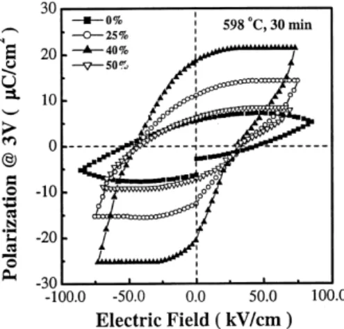
Fig. 7 illustrates the polarization vs. electric field curves recorded with y3 to q3 V excitations. The polarization of 40% OMR films with 598⬚C post an-nealing had the maximum remanent polarization and 2 Ec of 77 kVrcm. The remanent polarization and coercive field of the 25% and 40% OMR films with 598⬚C post-annealing were 23 Crcm2, 40 Crcm2 and 80 kVrcm, 77 kVrcm at an applied voltage of 3 V,
Ž .
respectively Fig. 8 . Moreover, the remanent polariza-tion and coercive field nearly attained saturapolariza-tion at over 3 V. We believe that these results indicated supe-rior properties of SBTN than those in other
investiga-w x
tions 8,12,16,17,23,25᎐27 . These excellent properties, possibly attributed to the unique solid solution of SrBi Ta O2 2 9 and SrBi Nb O , made the remanent2 2 9
polarization value of our SBTN films comparable with that of PZT.
Fig. 7. The polarization vs. electric field curves of various OMR SBTN films with 598⬚C post-annealing.
Fig. 8. The remanent polarization and coercive field of the 25% and 40% OMR SBTN thin films with 598⬚C post-annealing as a function of applied voltage.
Fig. 9 depicts the dependence of the dielectric con-stant and leakage current on the OMR for the films with 598⬚C post-annealing. The 40% OMR film had a dielectric constant of 752 at an applied voltage of 0 V and a leakage current of 6=10y6Arcm2at an electric field of 50 kVrcm with a time delay of 30 s. Although the dielectric constant and the leakage current in-creased with an increase in OMR, it reached a maxi-mum value at 40% OMR. According to this figure, further increasing the OMR decreased the dielectric constant and leakage current. The relation of polariza-tion P and dielectric constant could be obtainedr analytically using the following equation:
Ž . Ž .
Ps )o
H
y1 d Er 1where E is an applied field, and is the dielectrico
constant in free space. The SBTN films could exhibit a large dielectric constant due to polarization of electric dipoles. Hence, the 40% OMR thin films with 598⬚C post-annealing had a maximum dielectric constant due
Ž . Ž .
to strong 115 and 220 reflections of its XRD pattern ŽFig. 2b and its maximum remanent polarization..
The SBTN films exhibited a leakage current due to dielectric loss. The dielectric loss normally comes from two mechanisms: resistive loss and relaxation loss. In
Ž
the resistive loss mechanism, mobile charges electrons .
and holes in the film consume the energy. The case of relaxation loss, the mechanism is the relaxation of the dipole, which expends the energy. If the insulating film contains very few mobile charges, the relaxation loss
w x
would be the dominant mechanism 28 . According to a previous investigation, the most probable compensation with the substitution of Bi ions at the Sr site in Sr-defi-cient and Bi-excess SBTN is due to cation vacancies,
w x rather than changes in the cation valency 24 . The difference in valency between the Sr and Bi ions
ap-Fig. 9. The dependence of the dielectric constant and leakage cur-rent of the 598⬚C post-annealing films on the OMR.
peared to be attributable to compensation due to the change in the Bi ion valency in the Sr site, i.e.:
3q ⬘⬘ ⭈ ⭈ Ž .
Bi qV ªBi ªBi qhSr Sr Sr 2
where Bi3q, VSrY, Bi⭈Sr, BiSr and h⭈ represent the excess Bi ions, Sr vacancy, Bi ion on Sr site with charge, Bi ion on Sr site without charge and hole, respectively.
Ac-Ž .
cording to Eq. 2 , the SBTN material tends to show a p-type conductivity. Moreover, the conductivity is usually large, due to the holes produced with 20%
Sr-Ž . Ž .
deficient Srs0.8 and 25% Bi-excess Bi;2.5 in SBTN thin films.
High temperature deposition of SBTN films under non-oxidizing atmosphere, such as Ar, generally pro-duces oxygen vacancies in the film according to:
⭈⭈ Ž .
OolV q2 e⬘q1r2Oo 2 3
where O , Vo o⭈⭈ and e⬘ represent the oxygen ion on its normal site, oxygen vacancy and electron, respectively.
Ž .
According to Eq. 3 , the concentration of the electrons produced with the existence of oxygen vacancies is
w x
usually small when the OMR is increased 29᎐31 . In addition, the concentration of the oxygen vacancies in the perovskite oxide films is much smaller, i.e.
approxi-w x
mately 0.0001 M 32 . As expected, the concentration of holes in our high-OMR films was relatively higher than that of the electrons, which was attributed to the holes produced in the films with 20% Sr-deficient and 25% Bi-excess. Fig. 9 indicates that the leakage current density increased with an increase in OMR of up to 40%, which was possible owing to the reduction in concentration of the electrons in the films sputtered at higher OMR to compensate for the holes. According to Fig. 3, the Bi concentration decreased rapidly in the films deposited at above 40% OMR, which may be attributed to a decrease in the concentration of holes which decreased the leakage current density.
According to Fig. 9, the dielectric constant attains a maximum value at 40% OMR with 598⬚C post-anneal-ing, due to the maximum remanent polarization. In addition, although the leakage current increases with an increasing OMR, it attains a maximum value at 40% OMR, due to the change in ratio of electrons to holes in the SBTN films. Further increasing the OMR de-creases the leakage current, due to the decrease of the concentration of Bi in the SBTN films. Hence, the
Ž .
composition effect Sr-deficient and Bi-excess domi-nates the electrical properties of the films sputtered at various OMR.
The loss tangent and resistivity of the films are also a function of OMR, as shown in Fig. 10. The 40% OMR film had a loss tangent of 0.035 at 100 kHz. Both the minimum resistivity and maximum loss tangent occur-ring at 40% OMR correlated with the results in Fig. 10. In addition, the loss tangent was due to the leakage current loss by a parallel resistance. Moreover, the change in loss tangent was closely associated with the change in the resistivity and leakage current in the
Ž .
various OMR films Figs. 9 and 10 . Therefore, the conduction mechanism in these films would be resistive loss. Restated, the energy was consumed by mobile
Ž .
charges holes, electrons, and oxygen vacancies in the film. The variations of loss tangent and resistivity were closely related to the concentration change of mobile charges.
Fig. 11 summarizes the fatigue characteristics of the SBTN films deposited at 25, 40, and 50% OMR with 598⬚C post-annealing. The fatigue test was performed using a bipolar square wave of 3 V at 1 MHz. These exhibited only slight degradation of polarization at"3 V square wave after 1011 cycles. The results confirmed that the sputtered SBTN films did not experience any fatigue problem, which was commonly observed in PZT films. The measured value of Qs wspUypn was ap-proximately 20 Crcm2 for 40% OMR SBTN films with 598⬚C post annealing. Fig. 12 illustrates that the
Fig. 10. The dependence of the loss tangent and resistivity of the 598⬚C post-annealing films on the OMR.
Fig. 11. Polarization fatigue of the 25, 40 and 50% OMR SBTN films with 598⬚C post-annealing.
polarization of 25% and 40% OMR films was degraded by less than 0.5% per decade up to 240 min. A previous investigation revealed that the bulk ionic conductivities of SBTN were much higher than those of the
per-w x
ovskite ferroelectric, e.g. PZT 7 . The high ionic con-ductivities have allowed us to infer that the good fatigue resistance of SBTN was due to the easy recov-ery of defects. More specifically, oxygen vacancies en-trapped within the capacitors were easily released, re-sulting in a limited space charge buildup and domain wall pinning during the polarization reversal process w x7 . The ionic conductivities of SBTN with various OMR Ž;10y7 Srcm were much higher and close to the.
Ž .
electrical conductivities Fig. 10 .
Fig. 13a,b depict the leakage current, with a time delay of 30 s, of 25% and 50% OMR films with 598⬚C post annealing, under different 200-s stress fields. The leakage currents of 25% OMR films under 50, 100 and 200 kVrcm stress fields degraded, while those of 50% OMR films under 50 and 100 kVrcm stress fields did not degrade; however, degradation occurred in the
Fig. 12. Polarization of the 25% and 50% OMR SBTN films with 598⬚C post-annealing, as a function of retention time.
Fig. 13. The leakage current with delay time 30 s of SBTN films
Ž . Ž .
deposited at: a 25%; and b 50% OMR with 598⬚C post annealing as a function of electric field with 200 s stress.
films after exposure to a 200 kVrcm stress field. The leakage current degradation in 50% OMR films under 200 kVrcm was smaller than in 25% OMR films. Therefore, the dc reliability of SBTN films could be improved by high OMR deposition. The possible mobile charges for SBTN films were holes, electrons, and oxygen vacancies. The holes and electrons were only the transfer carriers and could not accumulate at the interface and grain boundaries. Hence, the entrapped oxygen vacancies degraded the leakage current of the SBTN films. The leakage current under a ‘low DC stress field’ did not degrade because the migration of oxygen vacancies was depressed by the grain boundary. The leakage current under a ‘high DC stress field’ degraded because the migration and creation of oxygen vacancies under a high DC stress field occurred. More-over, the migration of oxygen vacancies towards the cathode and the piling up of oxygen vacancies near the cathode definitely lowered the resistance of the Schot-tky junction, which would increase the leakage current. However, high OMR deposition can reduce the DC degradation of SBTN films.
Fig. 14a,b depicts the leakage current, with a time delay of 30 s, of 25% and 50% OMR films with 598⬚C
Fig. 14. The leakage current with delay time 30 s of SBTN films
Ž . Ž .
deposited at: a 25%; and b 50% OMR with 598⬚C post annealing as a function of electric field with a "10-V square wave ac stress frequency and 180 s stress.
post annealing, under a different "10 V square wave 180-s ac stress frequency. The leakage currents of 25% OMR films under 10, 100, 10 k and 100 kHz stress frequencies degraded, while those of 50% OMR films under 10, 100 and 10 kHz stress frequencies did not degrade; however, degradation occurred in the film after a 100-kHz stress frequency. Under the 100-kHz stress frequency, the leakage current degradation in the 50% OMR films was much smaller than in the 25% OMR films. Therefore, the ac reliability of SBTN films could also be improved by high OMR deposition. The oxygen vacancy was referred to as an electron trapping state, where the predominant charge exchange was between the conduction band and the trap level. Under ac stress applied at Schottky junction, the depletion layer width varied about its equilibrium position due to trapping and detrapping of electrons from the oxygen
w x
vacancies 33 . The ac degradation of SBTN films could be improved by higher OMR with less oxygen vacan-cies.
Lifetime extrapolation using constant voltage stress᎐
Ž .
time dependent dielectric breakdown TDDB studies ŽFig. 15 predicted the 10-year lifetime at a 1-V operat-.
ing voltage. Fig. 15 indicated that the characteristic Ž .
time tc h depended on the electric field. The character-Ž .
istic time tc h was defined as the time when the cur-rent density shows a value larger than the minimum by
Ž .
one order =10 under DC stress. The characteristic Ž .
time tc h increased with a decrease of the electric field. This finding suggested that the 50% OMR film has a longer lifetime than the 0, 25, and 40 OMR films. The TDDB, as shown in Fig. 15, was also referred to as the resistance degradation of dielectrics, which showed a slow increase of leakage current under DC field stress. Hence, the SBTN films degraded owing to the deteri-oration of Schottky interface barrier.
Available theories attempting to account for the degradation mechanism of perovskite titanates can be categorized as either grain boundary model or
reduc-w x
tion model 34 . In the grain boundary model, a DC field-induced deterioration of the grain boundaries is responsible for the degradation phenomenon. In the reduction model, the positively charged oxygen vacan-cies with a relative high mobility electromigrate to-wards the cathode under DC electric field. The oxygen vacancies then pile up at the front of cathode and are compensated for by the electron injected from cathode. The outcome is that the space charge accumulation at grain boundaries and interface of SBTN and metal reduces the grain boundary height and interface bar-rier height and, then, increases the leakage current. Results in this study are related to the grain boundary
Ž .
and reduction models, as follows: 1 the 50% OMR SBTN has more ‘grain boundaries’ than lower OMR SBTN because the grain size of 50% OMR SBTN is
Ž .
smaller Fig. 5b . Therefore, as expected, the 50% OMR SBTN has a longer lifetime on the basis of the grain boundary model, which was verified by the results
Ž .
in Fig. 15; and 2 the 50% OMR SBTN contains a low concentration of oxygen vacancies compared to 25% OMR film. Hence, the 50% OMR SBTN film has a smaller degradation and longer lifetime. On the basis
Fig. 15. Time to breakdown of the various OMR SBTN films with 598⬚C post-annealing as a function of stress field.
Ž
of three separate complex planes capacitance, .
impedance and admittance analyses, the defect densi-ties of 25% and 50% OMR films were 5.5=1016 and 1.7=1016cmy3, respectively. The 50% OMR SBTN had less defects than the 25% OMR sample. According to the prediction of reduction model, the deterioration of 50% OMR SBTN was smaller. In fact, the TDDB was significantly improved in the high OMR sample as
Ž .
compared to low OMR sample Fig. 15 .
4. Conclusions
This work investigated the effect of the annealing process on the ferroelectric properties of various OMR sputtered SBTN thin films. Experimental results indi-cated that annealing can effectively obtain a large remanent polarization. The remanent polarization, di-electric constant and leakage current of 598⬚C post-annealing SBTN thin films increased with an increase in the OMR and reached a maximum value at 40% OMR. Results obtained from the dielectric constant and the leakage current were interpreted on the basis of polarization effect and loss theory. The 400-nm thick 40% OMR SBTN films with 598⬚C post-annealing ex-hibited good surface morphology and had a dielectric constant of 752, a loss tangent of 0.035 at 100 kHz, a leakage current density of 6=10y6 Arcm2 at an elec-tric field of 50 kVrcm with a delay time of 30 s,
Ž . 2
remanent polarization 2 Pr of 40 Crcm and
coer-Ž .
cive field 2 Ec of 77 kVrcm at an applied voltage of 3 V. The 10-year lifetime of the time-dependent dielec-tric breakdown studies indicated that high OMR sam-ples have longer lifetime than the other lower OMR samples. The SBTN films demonstrated fatigue free characteristics up to 1011 switching cycles under a 3-V bipolar 1 MHz square wave. Moreover, the polarization of the films degraded less than 0.5% per decade up to 240 min.
Acknowledgements
The authors would like to thank the National Sci-ence Council of R.O.C. for financially supporting this research under Contract No. NSC 87-2112-M009-037.
References
w x1 J. Kudo, Y. Ito, S. Mitarai, N. Ogata, S. Yamazaki, H. Urashima, A. Okutoh, M. Nagata, K. Ishihara, Int. Electron. Devices
Ž . Meet. Tech. Dig. 34 1997 .
w x2 M. Takeo, M. Azuma, H. Hirano, K. Asari, N. Moriwaki, T. Otsuki, K. Tatsuuma, Int. Electron. Devices Meet. Tech. Dig.
Ž . 38 1997 .
w x3 R. Dat, H.D. Shih, in: R.K. Pandey, D.E. Witter, U. Varshneg ŽEds. , 99th Annual Meeting of the American Ceramic Society. Cincinnati, Ohio, U.S.A., May 4᎐7, 1997, Proceedings of the Symposium on Integrated Thin Films and Applications, , 1997, p. 1.
w x4 M. Suzuki, J. Ceram, Soc. Jpn. 103 1995 1088.Ž .
w x5 T. Mihara, H. Yoshimori, H. Watanabe, C.A.P.D. Araujo, Jpn. Ž .
J. Appl. Phys. 34 1995 5233.
w x6 D. Dimos, H.N.A. Shareef, W.L. Warren, B.A. Tuttle, J. Appl. Ž .
Phys. 83 1996 1682.
w x7 T.C. Chen, C.L. Thio, S.B. Desu, J. Mater. Res. 12 1997 2628.Ž . w x8 R. Dat, J.K. Lee, O. Auciello, A.I. Kingon, Appl. Phys. Lett. 67
Ž1995 572..
w x9 T. Kanehara, I. Koiwa, Y. Okada, K. Ashikaga, H. Katoh, K. Ž . Kaifu, Int. Electron. Devices Meet. Tech. Dig. 42 1997 . w x10 S.I. Ohfuji, M. Itsumi, Jpn. J. Appl. Phys. 37 1998 2559.Ž . w x11 D.J. Taylor, R.E. Jones, Y.T. Lii, P. Zurcher, P.Y. Chu, S.J.
Gillespie in: S.B. Desu, R. Ramesh, B.A. Tuttle, R.E. Jones, Ž .
I.K. Yoo Eds. , Ferroelectric Thin Films V, Pittsburgh, PA, Ž .
U.S.A., 1996, Mat. Res. Soc. Symp. Proc. 433 1996 97. w x12 I. Koiwa, K. Tani, J. Mita, T. Iwabuchi, Jpn. J. Appl. Phys. 37
Ž1998 192..
w x13 T. Osaka, A. Sakakibara, T. Seki, S. Ono, I. Koiwa, A. Ž .
Hashimoto, Jpn. J. Appl. Phys. 37 1998 597.
w x14 S.B. Desu, P.C. Joshi, S.O. Ryu, Appl. Phys. Lett. 71 1997Ž . 1041.
w x15 J. Zhu, X. Zhang, Y. Zhu, S.B. Desu, J. Appl. Phys. 83 1998Ž . 1610.
w x16 K. Miura, M. Tanaka, Jpn. J. Appl. Phys. 37 1998 606.Ž . w x17 H.M. Tsai, P. Lin, T.Y. Tseng, Appl. Phys. Letts. 72 1998Ž .
1787.
w x18 T. Horikawa, N. Mikami, T. Makita, J. Tanimura, M. Kataoka, Ž .
K. Sato, M. Nunoshita, Jpn. J. Appl. Phys. 32 1993 4126. w x19 M.S. Tsai, S.C. Sun, T.Y. Tseng, IEEE Trans. Electron. Devices
Ž . 46 1999 1829.
w x20 S.B. Desu, D.P. Vijay, X. Zhang, B. He, Appl. Phys. Lett. 69 Ž1996 1719..
w x21 I. Koiwa, T. Kanehara, J. Mita, T. Iwabuchi, T. Osaka, S. Ono, Ž .
Jpn. J. Appl. Phys. 36 1997 1597.
w x22 H. Watanabe, T. Mihara, H. Yoshimori, C.A.P.D. Araujo, Jpn. Ž .
J. Appl. Phys. 34 1995 5240.
w x23 T.C. Chen, T. Li, X. Zhang, S.B. Desu, J. Mater. Res. 12 1997Ž . 2165.
w x24 K. Miura, M. Tanaka, Jpn. J. Appl. Phys. 37 1998 2554.Ž . w x25 T. Noguchi, T. Hase, Y. Miyasaka, Jpn. J. Appl. Phys. 35 1996Ž .
4900.
w x26 H.M. Tsai, P. Lin, T.Y. Tseng, J. Appl. Phys. 85 1999 1095.Ž . w x27 Y.T. Kim, D.S. Shin, Appl. Phys. Lett. 71 1997 3507.Ž . w x28 P. Li, J.F. Mcdonald, T.M. Lu, J. Appl. Phys. 71 1992 5596.Ž . w x29 C.S. Hwang, S.O. Park, H.J. Cho, C.S. Kang, H.K. Kang, S.I.
Ž . Lee, M.Y. Lee, Appl. Phys. Lett. 67 1995 2819. w x30 R.M. Waser, J. Am. Ceram. Soc. 72 1989 2234.Ž .
w x31 D.M. Smyth, M.P. Harmer, P. Peng, J. Am. Ceram. Soc. 72 Ž1989 2276..
w x32 M.S. Tsai, T.Y. Tseng, Mater. Chem. Phys. 57 1998 47.Ž . w x33 Y. Fukuda, K. Numata, K. Aoki, A. Nishimura, Jpn. J. Appl.
Ž . Phys. 35 1996 5178.
w x34 R. Waser, T. Baiatu, K.H. Hardtl, J. Am. Ceram. Soc. 73 1990Ž . 1645.